Cd-doping a facile approach for better thermoelectric transport properties of BiCuSeO oxyselenides

M. U. Farooq*a, Sajid Butt*bc, Kewei Gaoa, YingCai Zhud, Xigui Suna, XiaoLu Panga, Sajid U. Khanb, Fida Mohmedc, Asif Mahmoode, Nasir Mahmood*f and Wei Xu*dg
aSchool of Materials Science and Engineering, University of Science and Technology Beijing, Beijing 100083, People’s Republic of China. E-mail: umerustb@yahoo.com
bDepartment of Materials Science and Engineering, Institute of Space Technology, Islamabad 44000, Pakistan. E-mail: sajidarif@hotmail.com
cState Key Laboratory of New Ceramics and Fine Processing, School of Materials Science and Engineering, Tsinghua University, Beijing 100084, People’s Republic of China
dBeijing Synchrotron Radiation Facility, Institute of High Energy Physics, Chinese Academy of Sciences, 100049, People’s Republic of China. E-mail: xuw@mail.ihep.ac.cn
eDepartment of Material Science and Engineering, College of Engineering, Peking University, Beijing 100871, China
fInstitute of Superconducting and Electronic Materials, Australian Institute of Innovative Materials, University of Wollongong, Squires Way, North Wollongong, NSW 2500, Australia. E-mail: nasirm38@gmail.com
gRome International Center for Materials Science, Superstripes, RICMASS, via deiSabelli 119A, I-00185 Roma, Italy

Received 20th January 2016 , Accepted 17th March 2016

First published on 18th March 2016


Abstract

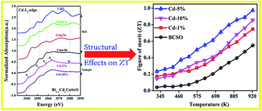
BiCuSeO-based thermoelectric materials have spurred tremendous interest among the thermoelectric community due to their ultra-low thermal conductivity and relatively large Seebeck coefficient (S). In this work, we have reported the effect of Cd-doping at the Bi site, instead of the previously studied Cu site, on the thermoelectric performance of BiCuSeO by modifying the insulating layer. While maintaining good phase purity, Cd was successfully doped at the Bi site as confirmed by X-ray absorption fine structure spectroscopy. The Cd-doping substantially improves the electrical conductivity by a factor of 20 through bond anharmonicity at room temperature while increasing the Cd concentration over 5%. Further, the incorporation of the lighter atom at the Bi site creates phonon scattering centers and results in weak bonding between the layers, resulting in a remarkable perturbation of the local geometric and electronic structure. BiCuSeO with 5% Cd-doping maintains a large S and a high electrical conductivity up to 923 K and exhibits the highest power factor values (600 μW m−1 K−2 at 323 K and 447 μW m−1 K−2 at 923 K) and the largest ZT (0.98 at 923 K). Cd-doping at the Bi site in p-type thermoelectric BiCuSeO was shown to be a very good technique for improving the thermoelectric performance and could be extended to other thermoelectric materials to enhance the efficiency of thermoelectric devices for energy-harvesting.


Introduction

Green energy is gaining more attention because of the environmental concerns and global warming issues associated with the consumption of fossil fuels but conversion efficiency is still a big issue. One of the major issues associated with the low efficiency of different energy systems is the loss of energy, such as heat production due to internal resistance. Thermoelectric materials are attracting immense attention because of their ability to direct the reversible inter-conversion of heat and electricity, which further makes thermoelectric materials strong candidates for green energy harvesting.1,2 The efficiency of green energy can be enhanced by designing a system which combines photovoltaic cells and thermoelectric technologies.3 The efficiency of a thermoelectric material is calculated as a dimensionless quantity called the figure of merit: ZT = S2σT/κ, where S, σ, κ and T represent the Seebeck coefficient, electrical conductivity, total thermal conductivity and the working temperature, respectively. Hence, the conversion efficiency of a thermoelectric material can be enhanced by increasing S2σ (power factor) and by reducing κ. Furthermore, κ is composed of the electronic thermal conductivity (κe) and the lattice/phonon thermal conductivity (κl). The term κe is associated with the electronic transport properties, and is directly proportional to the electrical conductivity. Therefore, the only possible way of reducing κ without altering the electronic transport properties is to suppress κl. Targeted fabrication of nanomaterials can effectively improve the transport properties with simultaneous control over κl without compromising κe.4 For efficient thermoelectric materials, the ZT value should be close to unity.5 Several approaches have been adopted in order to enhance the efficiency of thermoelectric materials like the introduction of layered materials which have an intrinsically low thermal conductivity,6 thereby, reducing the thermal conductivity; for instance, introducing nanocomposites7–10 nanostructured materials,11,12 assembling nano-wires13,14 superlattices15 and making thin films.16 Dresselhaus12 suggested that the introduction of nanoparticles leads to increased phonon scattering and hence, a decrease in thermal conductivity. Thus, phonon scattering can be increased by reducing the particle size to less than the mean free path of phonons. Recently, we have reported reduced thermal conductivity in an oxide (Ca3Co4O9) based composite by incorporating nanosize particles of La0.8Sr0.2CoO3 (ref. 17) and CdO.18 But improving the thermoelectric performance by incorporating nanoparticles has several issues as the introduction of nanoparticles also affects the electrical conductivity as well as phonon scattering. Thus, very good control over the particle size and its distribution is a hurdle for the practical application of nanocomposites. Meanwhile, natural superlattice materials have been gaining much attention because of their unique inherent physical properties.19,20 Optimizing the power factor of natural superlattice materials would improve the thermoelectric performance of the species. The p-type oxyselenide BiCuSeO thermoelectric material has a natural superlattice21 layered structure where the conducting (Cu2Se2)2− and insulating (Bi2O2)2+ layers are stacked alternatively22,23 and its intrinsic thermal conductivity is low due to the anharmonicity of lattice vibration. The carrier mobility of these materials is poor, which lowers the power factor value, however, previously several attempts have been made to improve the electrical conductivity by modifying the conductive and insulating layers either by introducing some vacancies24,25 or by making heterovalent substitutions.26–28 But, it is notable that by altering the insulating layer better results can be achieved when the Bi site is substituted by similar ionic sized elements with smaller atomic mass differences. Ohtani et al. proved the possibilities of the above mentioned consideration by showing that the p-type oxyselenide BiCuSeO material can be doped by elemental substitution at the Bi site or by introducing vacancies at the Cu site.29 However, the selection of doping elements at these positions is also a crucial issue; to date several elements have been adopted to improve the thermoelectric efficiency. A dopant that can further reduce the benchmark lower thermal conductivity, increase the electrical conductivity and has a higher carrier concentration along with better carrier mobility is highly desirable.

Here, we have reported the thermoelectric performance of Cd-doped BiCuSeO, which is synthesized by a two-step solid state reaction and spark plasma sintering (SPS). High energy ball milling was adapted to obtain a smaller grain size with a large number of grain boundaries as well as replacing the Bi atoms with Cd ones homogenously. The SPS sintering was done to reach the theoretical density. As a result the concentration of the hole-type charge carrier increased by replacing the Bi3+ ions with Cd2+ ones, which caused a dramatic enhancement in the electrical conductivity. For instance, the electrical conductivity was improved from 10 to 160 S cm−1 at room temperature by Cd-doping up to 5% in the matrix of BiCuSeO due to through bond anharmonicity as a result of the increased hole concentration by Cd doping which resulted in a high PF of 600 μW m−1 K−2 for 5%-Cd doping. Furthermore, the substitution of Cd2+ ions with smaller atomic mass in the lattice of BiCuSeO induces atomic point defects and high grain boundaries produced by the high energy ball milling acting as phonon scattering centres to suppress the thermal conductivity without compromising the power factor. Ultimately, a large power factor of up to 446 μW m−1 K−2 at 923 K and a suitably reduced lattice thermal conductivity resulted in a ZT value of up to 0.98 at 923 K which is about 80% higher than that obtained for its pure counterpart. Thus, we believe that the methodology developed in the present study to dope the heteroatom at the Bi site will be very promising for improving the performance of thermoelectric materials for high efficiency energy devices.

Experimental details

Synthesis process

A series of compositions of Bi1−xCdxCuSeO (x = 0.01, 0.05 and 0.1) were fabricated by a two-step solid state reaction. Stoichiometric amounts of Bi (4 N), Bi2O3 (4 N), Cd (4 N), Cu (5 N) and Se (5 N) powders were mixed by high energy ball milling at 350 RPM for 5 hours, in ethanol under vacuum to avoid any side-reaction. The mixed powders were compacted into pellets using a cold press and were sealed in evacuated quartz tubes. The sealed pellets were annealed in a furnace first at 573 K for 8 hours and then at 873 K for 24 hours. The annealed samples were crushed in a pestle and mortar and then subsequent ball milling at 450 RPM for 5 hours. A few drops of poly-vinyl alcohol (PVA) were added to maintain the compact shape and to avoid breakage. The obtained powders were compacted by SPS sintering under a uniaxial pressure of 50 MPa for 6 minutes to obtain the high density close to the theoretical one for high performance. Each pellet was cut into a rectangular rod of dimensions 15 × 3 × 3 mm3 and a square pellet of diameter ϕ = 10 mm to carry out the different measurements.

Physical characterization

The crystal structures of all the specimens were investigated by means of X-ray diffraction (XRD) using an analytical X’pert diffractometer (Tokyo, Japan) with Cu-Kα radiations (λ = 0.15406 nm). The lattice parameters were calculated by a least square refinement method using MD jade 5.0. The surface morphology was analyzed using a scanning electron microscope (SEM Zeiss Evo 18 Germany). The morphological and selected area electron diffraction (SAED) characterizations of the as-synthesized samples was achieved means of transmission electron microscopy (TEM) with an FEI Tecnai T20 microscope. X-ray absorption fine structure spectroscopy (XAFS) was carried out using the 4B7A beamline30 of the Beijing Synchrotron Radiation Facility. The electron in the storage ring was 2.5 GeV with the accumulated current injected constantly in the top-up mode at 250 mA. Cd L3-edge XAFS spectra of Bi1−xCdxCuSeO (x = 5%, and x = 10%) were recorded in the fluorescence mode with a good S/N ratio. The incident X-ray was monochromatized by the Si (111) double crystal monochromator. Both samples and the head of the SDD fluorescence detector were housed in a low vacuum chamber, which was pumped to 1.3 × 10⁻² Pa before measurements were carried out in order to eliminate the absorption of fluorescent photons by air. Raw X-ray absorption near-edge spectra (XANES) were normalized to the unit edge jump after subtracting the atomic absorption background using the IFEFFIT-Demeter package.31 The theoretical Cd L3 XANES spectra were calculated using the FEFF9 code within the full multiple scattering theory. To simulate the doping site, the Cd atoms were set at the central atomic site of Bi, Cu and Se, respectively, while keeping the original atomic coordinates as in the BiCuSeO. The radius of the atomic cluster for SCF potential calculation and multiple scattering clusters for FMS were optimized as 5 Å and 10 Å, respectively. The Hedin–Lundqvist exchange correlation was adopted and no additional parameters were used.

Thermoelectric transport properties

Rectangular specimens were used to measure the S and the electrical conductivity, simultaneously, by LINSEIS LSR-3 (Seebeck & electric resistivity unit) from room temperature to 923 K. The thermal diffusivity (D) and the heat capacity (Cp) were measured, simultaneously, by Netzsch LFA 457 using the laser flash method along the thickness direction of the square pellets. The total thermal conductivity (κ) was calculated using the following formula: κ = DCpd, where, d is the mass density measured by the Archimedes principle. Considering the anisotropic nature of BiCuSeO, all the electrical and thermal transport properties were measured in the same direction.32 The density of all the samples ranged from 8.795–8.825 which is about 88% of the theoretical density. The carrier concentration, mobility and Hall coefficients were measured at room temperature using the Ecopia Hall measurement system (HMS-3000).

Results and discussion

The crystal structure and phase purity of the developed samples were investigated using XRD analysis, as shown in Fig. 1a. The pure BiCuSeO and Cd-doped BiCuSeO with different doping concentrations (1%, 5% and 10%) delineated a single phase tetrahedral crystal structure as indexed by PDF#82-1073 (ZrSiCuAs type structure). Previous reports on doped BiCuSeO have shown that elemental doping at the Bi site generally leads to a Bi2O3 impurity phase, which can affect the phase purity and thermoelectric performance of the materials by effecting the mobility of the charge carriers and lowering the electrical conductivity.6,33 Similarly, doping of Cd at the Cu site also results in the formation of additional phases as impurities to BiCuSeO, especially at higher doping concentrations due to the significant difference between the ionic radii of Cd2+ (0.95 Å) and Cu+ (0.77 Å).34 However, it is worth noting here that no detectable impurity phase was found which provides assurance of the successful control of the structure and phase during the doping of Cd. The smaller ionic radii of Cd2+ (0.95 Å) than Bi3+ (1.03 Å) further assures the feasibility of Cd-doping at the Bi site compared to the Cu site, as well as having no effect on the phase but it can weaken the bonding between the two layers. Further, a small shift of 2θ towards the higher angle was observed in all the Cd-doped BiCuSeO samples due to the smaller ionic radii of Cd2+ compared to that of Bi3+, which confirms the doping of Cd in the lattice of BiCuSeO at the Bi site with better control over crystal structure and phase purity.
image file: c6ra01686c-f1.tif
Fig. 1 (a) XRD patterns of pure and Cd-doped BiCuSeO with different weight ratios of Cd (1%, 5% & 10%) and (b) effects of Cd-doping concentrations on lattice parameters of BiCuSeO.

Fig. 1b represents the lattice parameters of pure BiCuSeO and Cd-doped BiCuSeO at different concentrations, it is clear that Cd-doping results in structural variation in the layered structure of BiCuSeO. The effect of the Cd-doping is more pronounced for the lattice parameter c than for a. It is interesting to note that with an increasing dopant content parameter a decreases, while parameter c increases. The reduction in a is associated with the smaller ionic radius of Cd2+ compared to that of Bi3+ (ref. 35) which confirms that Cd has replaced the larger sized atom (Bi) instead of the smaller sized atom (Cu), thereby confirming our hypothesis regarding the replacement of Bi in the insulating layer to enhance the electrical conductivity and to lower the thermal conductivity. However, the expansion in c can be attributed to weakening of the coulombic forces between the layers due to the Cd-doping in BiCuSeO.36 Thus, increasing the concentration of Cd results in weaker coulombic forces that redistribute the charges on each layer as [(Bi1−xCdx)O2]2(1−x)+ and [Cu2Se2]2(1−x)− calculated using electron count, thereby increasing the overall number of charge carriers. In fact, Cd-doping gives rise to holes in the modified conducting layers [Cu2Se2]2(1−x)−, resulting in reduced attractive forces between the layers and leading to an expansion in the c axis. Hence, the replacement of Cd at the Bi site creates phonon scattering centres by producing defects and redistribution of the charges in both layers thereby increasing the charge carriers and their mobility, and resulting in enhanced electrical and lower thermal conductivity, and consequently an improved ZT value. To observe the morphology and microstructure of the pure BiCuSeO and Cd-doped BiCuSeO, fractographs of the freshly broken cross sections of pure BiCuSeO and Cd-doped BiCuSeO pellets were obtained using SEM after SPS sintering as shown in Fig. 2. From Fig. 2, it is clear that the grain size of the Cd-doped BiCuSeO is smaller (Fig. 2b) than that of pure BiCuSeO, larger grains of which can be observed in the SEM image (Fig. 2a). These results confirm that Cd-doping reduced the grain size and resulted in a larger number of grain boundaries which would be very helpful for phonon scattering to lower the thermal conductivity. The reduced grain size might be due to the suppressed growth with Cd doping; hence grain size reduction leads to a higher grain boundary area. Moreover, a lath-like grain morphology was observed at a high density ranging from 8.795–8.825 after SPS treatment. In the experimental section it was shown that the density slightly decreased with increased Cd contents. The nanopores are probably the reason for the observed decreased values. Additionally, void-like-defects were present in the doped BiCuSeO (Fig. 2b) which are more prominent at the moderate dopant concentration but start diminishing at higher concentrations (Fig. 2d). These void-like-defects play a very critical role in breaking the strong attraction between the layers, increase the charge carrier mobility and enhance the electrical conduction and phonon scattering to lower the thermal conductivity, thereby, resulting in better thermoelectric properties. Further, a smaller grain size was also observed by TEM, as shown in Fig. 2e. The electron diffraction pattern presented in Fig. 2f verifies the layered structure of the Cd-doped BiCuSeO. Furthermore, clear Bragg spots in the SAED pattern confirm the doping of Cd in the lattice of BiCuSeO, which is in accordance with the XRD results. However, small splitting of the Bragg spots might be attributed to the size/mass difference of Cd and Bi atoms which change the lattice constants, as explained above. Thus, these structural studies have confirmed the modification of the conductive and insulating layers through heteroatom doping and vacancies or/and point defects in the conductive layers which redistribute the charges on both layers. Redistribution of the charges on the conductive [Cu2Se2]2(1−x)− and insulating [(Bi1−xCdx)O2]2(1−x)+ layers along with the phonon scattering centres in the lattice of the Cd-doped BiCuSeO are important in improving thermoelectric performance.


image file: c6ra01686c-f2.tif
Fig. 2 SEM fractographs of (a) pristine BiCuSeO, (b) 1% Cd-doped BiCuSeO, (c) 5% Cd-doped BiCuSeO and (d) 10% Cd-doped BiCuSeO. (e) TEM image and (f) SAED pattern of 5% Cd-doped BiCuSeO.

As the Cd-doping site has a greater effect on the properties of BiCuSeO, XAFS was utilized to identify the doping site of Cd in the lattice of BiCuSeO in order to understand its effects on the properties of BiCuSeO. The scattering of the outgoing photon-excited electrons by coordinate atoms modifies the spectral features; therefore, XANES spectra can be used as fingerprints of the local structural environment. The Cd L3-edge XANES spectra probe the transition from 2p to nd states of Cd, as shown in Fig. 3. The experimental spectra for Cd-5% and Cd-10% are almost identical, indicating the same coordinate environment of Cd in both samples. The spectral features from A1 to A4 originate from both the electronic structure as well as the geometric configuration of the coordinate atoms. Meanwhile, the feature B is mainly contributed by geometric structure. To identify the doping site, a qualitative comparison of the spectral features of the experimentally obtained spectra with that of the reference was carried out for all of the samples. Herein, two sets of references were used; one was the theoretical reference describing Cd at the Bi, Cu, and Se site of BiCuSeO and the other was an experimental spectrum of CdO, which could easily be formed in oxide thermoelectric materials.37 The spectrum of Cd@Bi looks more like the experimental spectra of Bi1−xCdxCuSeO than that of the other references. On the other hand, feature A3 in the experimental spectrum is less pronounced than in the theoretical Cd@Bi spectrum. This highlights that there is a local structural distortion upon the substitution of Bi by Cd. Nevertheless, it is evident from the XANES spectra that the Cd atoms indeed occupy the Bi site in the BiCuSeO lattice. Thus, verifying our previous conclusion from XRD and SAED, which consequently emphasized the hypothesis of structural and electronic tuning of BiCuSeO by Cd-doping to improve the electronic conduction while suppressing the thermal conductivity to obtain higher ZT values.


image file: c6ra01686c-f3.tif
Fig. 3 (a) The comparative XANES spectra of the Cd L3-edge of Cd-doped BiCuSeO with experimental and theoretical reference spectra; the experimental reference spectrum is for CdO while the theoretical reference spectra were calculated for Cd at Bi, Se, and Cu site of BiCuSeO, respectively. (b) The room temperature electrical transport properties as a function of Cd-doping fraction.

The better control over structure and phase after Cd-doping in the lattice of BiCuSeO makes it a good candidate for thermoelectric devices. Therefore, initially the electrical transport properties of pristine and Cd-doped BCSO as a function of doping contents (x) was measured at room temperature as shown in Fig. 3b. The electrical conductivity was enhanced with increased doping percent up to 5% and then reduced slightly, possibly because of lower mobility. The electrical conductivity at 5% doping was higher than that for pure BCSO by a factor of 20 due to the bond anharmonicity, while the S was positive for the entire specimen indicating its p-type nature. However, the reduction of S with increasing doping content was moderate as compared to the electrical properties. The combination of high electrical properties with moderate S, resulted in a significantly higher PF. Especially at 5% doping, the PF was 600 μW m−1 K−2 which is about 5 times higher than that for pure BiCuSeO. So, enhanced electrical transport properties at room temperature further verified our doping strategy as an excellent tool to improve the thermoelectric applications of BiCuSeO. Thus, prior to evaluating the heat transfer and ZT values electrical conductivity measurements as a function of temperature were carried out, as shown in Fig. 4a. The electrical conductivity of pure and lower dopant samples followed semiconducting behaviour, while with higher dopant contents σ decreased with increasing temperature indicating metallic behaviour as shown in Fig. 4a. Meanwhile, increasing the dopant concentrations improved the electrical conductivity due to the increased carrier concentrations which is consistent with the relation σ = neμ, which shows a direct relation of electrical conductivity σ with carrier concentration n and their mobility μ. This enhancement can be further explained by the presence of increased carriers in the conductive layers and the negative charge in the insulating layers and Cd-doping on the Bi site, which is also consistent with the behavior of LaFeAsO superconductors.38,39 The highest electrical conductivity of 73 S cm−1 was obtained for 5% Cd-doping at 923 K and this value was about 110% higher than that for the pure BiCuSeO. There was little difference between the electrical conductivities for 5% and 10% Cd doped BiCuSeO owing to the increased concentration and decreased mobility of charge carriers upon doping (Fig. 4b). From Fig. 4b, it is clear that with an increase in the dopant (Cd) concentration the number of charge carries increased but the mobility decreased. Thus, an appropriate dopant concentration is necessary to modify the electrical properties with a larger carrier along with better mobility. Fig. 4b shows that 5% Cd-doping results in the the greatest number of charge carriers with better mobility but as the dopant concentration was increased to 10% the number of charge carriers increased and the mobility decreased and there was no further increase in the electrical conductivity. That’s why BiCuSeO with 5% Cd-doping results in the greatest increase in the electrical conductivity.


image file: c6ra01686c-f4.tif
Fig. 4 Spectra of (a) temperature dependent electrical conductivity, (b) room temperature carrier mobility and carrier concentration, (c) temperature dependent Seebeck coefficient and (d) power factor for all the pure and Cd-doped BiCuSeO.

S as a function of temperature is shown in Fig. 4c. The positive S values for all the samples indicates that all of the samples exhibit p-type conduction behaviour. The decrease in S could be associated with an increased carrier concentration which can be estimated from the following equation for degenerate semiconductors:40

 
image file: c6ra01686c-t1.tif(1)
where m* is the carrier’s effective mass, e is electronic charge, h is the Planck’s constant, KB is the Boltzmann constant, T is the temperature and n is the carrier concentration. The above expression shows an inverse relation for S with n and a direct relation with temperature. With increasing dopant content, the carrier concentration increased, as explained above, which resulted in a decreased S value. For instance, the S of pristine BiCuSeO was 361 μV K−1 and 297 μV K−1 at room temperature and 923 K, respectively; while the S of Cd doped species was lower, e.g. 154 μV K−1 at 323 K and 231 μV K−1 at 923 K for 10% Cd-doped BiCuSeO. This observation is consistent with increased carrier concentration from the relation shown in eqn (1). Regarding the temperature dependence of S, the S values decreased with increasing temperature for relatively lower doping concentrations (ca. 1%), while at higher doping contents S increased with temperature. The temperature dependence of S is also consistent with the electrical conductivity trend following eqn (1). The combined effect of increased electrical conductivity and the moderate S values resulted in a high power factor of 600 μW m−1 K−2 at 323 K and 450 μW m−1 K−2 at 923 K for the 5% Cd-doped BiCuSeO, which was about 45% higher than that for BiCuSeO at 923 K (308 μW m−1 K−2 at 923 K), as shown in Fig. 4d. Thus, the improved electrical conductivity and higher power factor values of Cd-doped BiCuSeO than for pure BiCuSeO have proved the advantage of Cd-doping at the Bi site in the BiCuSeO lattice resulting in modified conductive and insulating layers along with higher charge carries and moderate carrier mobility values. Further, the band structure of BiCuQO (Q = S, Se, Te) consists of mixed heavy and light mass bands present in the top of the valance band that indicates the properties of good thermoelectric materials where heavier mass band leads to higher Seebeck coefficient while light mass associated with high electrical conductivity.41,42

To see the effect of larger grain boundaries and defects created by the Cd-doping in the lattice of BiCuSeO on phonon scattering to lower the thermal conductivity, thermal conductivity measurements were carried out as the function temperature, shown in Fig. 5a. The total thermal conductivity of all the samples decreased with increasing temperature and the lowest total thermal conductivity of 0.38 W m−1 K−1 at 923 K was obtained for 10% Cd-doped BiCuSeO, which is almost 25% lower than that for the pure BiCuSeO. A small increase was observed near 500 K which might be due to conversion of PVA to carbon as an impurity. The inset of Fig. 5a represents the thermal diffusivity which decreased with increasing temperature and dopant percent. On the other hand, heat capacity slightly increased with temperature as shown in the inset of Fig. 5c. Fig. 5b shows the electronic thermal conductivity which was derived from the Weidman–Franz law: κe = L0σT, where σ is the electrical conductivity, T is the working temperature and L0 is the Lorentz number. Generally, the Lorentz number value was constant for all of the materials because it changed slightly, but for most of the semiconductors, its variation at high temperature was significant. So, the Lorentz number was approximated from the expression given below,43

 
image file: c6ra01686c-t2.tif(2)
here, η represents the reduced Fermi energy, r is the scattering parameter and KB is Boltzmann constant. The η can be calculated from the following formula,
 
image file: c6ra01686c-t3.tif(3)


image file: c6ra01686c-f5.tif
Fig. 5 Spectra of (a) temperature dependent total thermal conductivity (the inset shows the trend of diffusivity with temperature), (b) electronic thermal conductivity as a function of temperature, (c) temperature dependent lattice thermal conductivity with estimated kmin (the inset shows heat capacity as a function of temperature) and (d) temperature dependent ZT value (the inset shows the effect of different dopant concentration at 323 K and 923 K on ZT) for all the pure and Cd-doped BiCuSeO.

The above equation is dependent on the nth order Fermi level which can be calculated as,

 
image file: c6ra01686c-t4.tif(4)
 
image file: c6ra01686c-t5.tif(5)

By putting the value of r = −1/2 (ref. 44) and η in the equation and using the approximation that acoustic phonon scattering is the major carrier scattering,36 the actual Lorentz number was calculated and was used to measure the electronic thermal conductivities for all of the samples. The decrement in overall thermal conductivity κ is associated with the decrease in lattice thermal conductivity, as shown in Fig. 5c. A minimum lattice thermal conductivity of 0.29 W m−1 K−1 was observed for the 10% Cd-doped BiCuSeO which is almost 50% lower than that for the pure BiCuSeO. For the BiCuSeO system, the lowest lattice thermal conductivity value can be estimated using Cahill’s approximation,45 which is given as,

 
image file: c6ra01686c-t6.tif(6)
where K is the Boltzmann constant, V is the volume per unit atom calculated for the tetrahedral phase of BiCuSeO, vt (1900 m S−1) and vl (320 m S−1) are the transverse and longitudinal components of sound velocity, respectively.46 The predicted kmin value of 0.59 W m−1 K−1 reduced to 0.42 W m−1 K−1 at 923 K for BiCuSeO and further reduced to the lowest value of 0.29 W m−1 K−1 obtained for 10% Cd-doped BiCuSeO, as shown in Fig. 5c. The factors affecting the point defects might be due to the atomic size differences between the dopant and substituent, atomic mass variations and the lattice size of the host structure.46–48 In the present case, a high mass fluctuation caused by the different atomic masses of Bi (209 g mol−1) and Cd (112.4 g mol−1) and the slight difference between their ionic radii (Cd ≈ 0.95 Å and Bi ≈ 1.03 Å) were collectively responsible for the enhancement of the point defects, resulting in enhanced phonon scattering to suppress the lattice thermal conductivity to even lower than kmin. In addition, the doping of Cd resulted in larger grain boundaries, which resulted in enhanced phonon scattering and consequently lowering of the thermal conductivity.

Finally, keeping practical applications in mind, ZT values were calculated to explore the effect of Cd-doping on the thermoelectric properties of BiCuSeO. Fig. 5d shows the temperature dependent ZT values for all the samples from 323 K to 923 K and it can be seen that with Cd-doping, the ZT value increased which is the combined result of the better electrical conductivity, enhanced power factor and the suppressed thermal conductivity. The high ZT value of 0.98 was achieved with 5% Cd-doped BiCuSeO, which is about 80% higher than that for the pure BiCuSeO system. Furthermore, from the inset of Fig. 5d, it can be observed clearly that at 323 K, there is no significant increase in ZT with increasing doping level but at 923 K the improvement in ZT value is significant. The improved ZT value is higher than that of many other doping systems such as Sr, Ag, Mg, Zn, La and Na on the Bi site.28,36,49–52 However, our presented ZT value is lower than that for Ba doping on the Bi site.22 The high ZT value is based on several controlled factors such as electrical and thermal conductivity, because of high concentration with better carrier mobility and the presence of phonon scattering centres. The 80% higher ZT value of Cd-doped BiCuSeO compared to the value obtained for pure BiCuSeO confirmed that our methodology, which involved substitution of Cd at the Bi site, is an attractive approach for improving the ZT value of thermoelectric materials. In addition, maintaining a layered structure with weaker interactions along with pure phase growth is a commonly faced challenge which has been overcome by this research.

Conclusions

In summary, we have developed a facile methodology to improve the thermoelectric performance of BiCuSeO through Cd-doping at the Bi site in the BiCuSeO crystal lattice. Pure BiCuSeO along with different doping contents of Cd were synthesized by solid state reaction using high energy ball milling followed by SPS. The structural study demonstrated that Cd was successfully doped at the Bi site without forming any impurity phase. Moreover, the doping site of Cd was evidently identified by the Cd L3-edge XANES spectra. A significant increase of up to 45% in power factor has been observed due to the high electrical conductivity of up to 110% and the moderate S for Cd-doped BiCuSeO. Further, suppressed lattice thermal conductivity was observed for Cd-doped BiCuSeO which was up to 50% lower than that for pure BiCuSeO due to the mass fluctuation caused by different atomic masses of Bi and Cd as well as the slight difference in the ionic radii, which causes point defect as phonon scattering centres. A maximum ZT of 0.98 was observed for the sample with 5% Cd-doped BiCuSeO at 923 K which is about 80% higher than that for pure BiCuSeO. Thus, it is believed that the Cd-doped BiCuSeO system is a promising candidate for p-type thermoelectric materials for energy harvesting applications. Low charge carrier mobility at higher doping concentrations leaves room for further enhancement in the thermoelectric efficiency of this material which could be achieved by the increasing carrier mobility by modifying both the conductive and charge reservoir layers.

Acknowledgements

We acknowledge the beam time granted by the Beijing Synchrotron Radiation Facility and the excellent technical support from the 4B7A beamline staff including Kun Tang, Chenyan Ma and Lei Zheng. We are also grateful for financial support from the National Science Foundation of China under grant No. U1532128. We are thankful to H. Z. Zhao and S. M. Li from the Institute of Physics, Chinese Academy of Science for their help regarding Seebeck coefficient measurements.

Notes and references

  1. T. M. Tritt and M. A. Subramanian, MRS Bull., 2006, 31, 188–198 CrossRef.
  2. T. M. Tritt, Encyclopedia of Materials: Science and Technology, Elsevier, 2002, pp. 1–11 Search PubMed.
  3. M. Fisac, F. X. Villasevil and A. M. López, J. Power Sources, 2014, 252, 264–269 CrossRef CAS.
  4. D. G. Cahill, K. Goodson and A. Majumdar, J. Heat Transfer, 2002, 124, 223 CrossRef CAS.
  5. J.-F. Li, W.-S. Liu, L.-D. Zhao and M. Zhou, NPG Asia Mater., 2010, 2, 152–158 CrossRef.
  6. L. D. Zhao, D. Berardan, Y. L. Pei, C. Byl, L. Pinsard-Gaudart and N. Dragoe, Appl. Phys. Lett., 2010, 97, 092118 CrossRef.
  7. C. Godart, A. P. Gonc, E. B. Lopes and B. Villeroy, Proceedings: Spring meeting MRS 2009, San Francisco, USA, 2009 Search PubMed.
  8. H. Pang, Y.-Y. Piao, Y.-Q. Tan, G.-Y. Jiang, J.-H. Wang and Z.-M. Li, Mater. Lett., 2013, 107, 150–153 CrossRef CAS.
  9. M. U. Farooq, S. Butt, K. Gao, X. Sun, X. Pang, S. U. Khan, W. Xu, F. Mohmed, A. Mahmood and N. Mahmood, Ceram. Int., 2016, 42, 8395–8401 Search PubMed.
  10. M. U. Farooq, S. Butt, K. Gao, X. Sun, X. Pang, A. Mahmood, W. Mahmood, S. U. Khan and N. Mahmood, Sci. China Mater., 2016, 59, 1–9 Search PubMed.
  11. C. J. Vineis, A. Shakouri, A. Majumdar and M. G. Kanatzidis, Adv. Mater., 2010, 22, 3970–3980 CrossRef CAS PubMed.
  12. M. S. Dresselhaus, G. Chen, M. Y. Tang, R. G. Yang, H. Lee, D. Z. Wang, Z. F. Ren, J.-P. Fleurial and P. Gogna, Adv. Mater., 2007, 19, 1043–1053 CrossRef CAS.
  13. A. I. Hochbaum, R. Chen, R. D. Delgado, W. Liang, E. C. Garnett, M. Najarian, A. Majumdar and P. Yang, Nature, 2008, 451, 163–167 CrossRef CAS PubMed.
  14. A. I. Boukai, Y. Bunimovich, J. Tahir-Kheli, J.-K. Yu, W. A. Goddard III and J. R. Heath, Nature, 2008, 451, 168–171 CrossRef CAS PubMed.
  15. T. C. Harman, Science, 2002, 297, 2229–2232 CrossRef CAS PubMed.
  16. R. Venkatasubramanian, Nature, 2001, 413, 597–602 CrossRef CAS PubMed.
  17. S. Butt, W. Xu, M. U. Farooq, G. K. Ren, F. Mohmed, Y. Lin and C.-W. Nan, J. Am. Ceram. Soc., 2015, 98(4), 1230–1235 CrossRef CAS.
  18. S. Butt, W. Xu, W. Q. He, Q. Tan, G. K. Ren, Y. Lin and C.-W. Nan, J. Mater. Chem. A, 2014, 2, 19479–19487 CAS.
  19. I. Terasaki, Y. Sasago and K. Uchinokura, Phys. Rev. B: Condens. Matter Mater. Phys., 1997, 56, R12685–R12687 CrossRef CAS.
  20. M. K. Wu, J. R. Ashburn, C. J. Torng, P. H. Hor, R. L. Meng, L. Gao, Z. J. Huang, Y. Q. Wang and C. W. Chu, Phys. Rev. Lett., 1987, 58, 908–910 CrossRef CAS PubMed.
  21. L.-D. Zhao, J. He, D. Berardan, Y. Lin, J.-F. Li, C.-W. Nan and N. Dragoe, Energy Environ. Sci., 2014, 7, 2900–2924 CAS.
  22. H. Hiramatsu, H. Yanagi, T. Kamiya, K. Ueda, M. Hirano and H. Hosono, Chem. Mater., 2007, 20, 326–334 CrossRef.
  23. C. Barreteau, L. Pan, E. Amzallag, L. D. Zhao, D. Berardan and N. Dragoe, Semicond. Sci. Technol., 2014, 29, 64001 CrossRef.
  24. Z. Li, C. Xiao, S. Fan, Y. Deng, W. Zhang, B. Ye and Y. Xie, J. Am. Chem. Soc., 2015, 137, 6587–6593 CrossRef CAS PubMed.
  25. Y. Liu, L.-D. Zhao, Y. Liu, J. Lan, W. Xu, F. Li, B.-P. Zhang, D. Berardan, N. Dragoe, Y.-H. Lin, C.-W. Nan, J.-F. Li and H. Zhu, J. Am. Chem. Soc., 2011, 133, 20112–20115 CrossRef CAS PubMed.
  26. F. Li, T.-R. Wei, F. Kang and J.-F. Li, J. Mater. Chem. A, 2013, 1, 11942–11949 CAS.
  27. J. Li, J. Sui, Y. Pei, C. Barreteau, D. Berardan, N. Dragoe, W. Cai, J. He and L.-D. Zhao, Energy Environ. Sci., 2012, 5, 8543 CAS.
  28. J. Li, J. Sui, Y. Pei, X. Meng, D. Berardan, N. Dragoe, W. Cai and L.-D. Zhao, J. Mater. Chem. A, 2014, 2, 4903 CAS.
  29. T. Ohtani, Y. Tachibana and Y. Fujii, J. Alloys Compd., 1997, 262–263, 175–179 CrossRef CAS.
  30. L. Zheng, Y. D. Zhao, K. Tang, C. Y. Ma, C. H. Hong, Y. Han, M. Q. Cui and Z. Y. Guo, Spectrochim. Acta, Part B, 2014, 101, 1–5 CrossRef CAS.
  31. B. Ravel and M. Newville, J. Synchrotron Radiat., 2005, 12, 537–541 CrossRef CAS PubMed.
  32. J. Sui, J. Li, J. He, Y.-L. Pei, D. Berardan, H. Wu, N. Dragoe, W. Cai and L.-D. Zhao, Energy Environ. Sci., 2013, 6, 2916–2920 CAS.
  33. F. Li, J.-F. Li, L.-D. Zhao, K. Xiang, Y. Liu, B.-P. Zhang, Y.-H. Lin, C.-W. Nan and H.-M. Zhu, Energy Environ. Sci., 2012, 5, 7188 CAS.
  34. S. D. N. Luu and P. Vaqueiro, Semicond. Sci. Technol., 2014, 29, 064002 CrossRef.
  35. R. D. Shannon, Acta Crystallogr., Sect. A: Found. Crystallogr., 1976, 32, 751–767 CrossRef.
  36. C. Barreteau, D. Bérardan, E. Amzallag, L. Zhao and N. Dragoe, Chem. Mater., 2012, 24, 3168–3178 CrossRef CAS.
  37. J. J. Rehr, J. J. Kas, F. D. Vila, M. P. Prange and K. Jorissen, Phys. Chem. Chem. Phys., 2010, 12, 5503 RSC.
  38. P. Quebe, L. J. Terbüchte and W. Jeitschko, J. Alloys Compd., 2000, 302, 70–74 CrossRef CAS.
  39. Y. Kamihara, T. Watanabe, M. Hirano and H. Hosono, 2008, 3296–3297.
  40. H. Wang, Y. Pei, A. D. LaLonde and G. J. Snyder, Proc. Natl. Acad. Sci. U. S. A., 2012, 109, 9705–9709 CrossRef CAS PubMed.
  41. D. Zou, S. Xie, Y. Liu, J. Lin and J. Li, J. Mater. Chem. A, 2013, 1, 8888–8896 CAS.
  42. D. J. Singh and I. I. Mazin, Phys. Rev. B: Condens. Matter Mater. Phys., 1997, 56, R1650–R1653 CrossRef CAS.
  43. W.-S. Liu, Q. Zhang, Y. Lan, S. Chen, X. Yan, Q. Zhang, H. Wang, D. Wang, G. Chen and Z. Ren, Adv. Energy Mater., 2011, 1, 577–587 CrossRef CAS.
  44. S. Johnsen, J. He, J. Androulakis, V. P. Dravid, I. Todorov, D. Y. Chung and M. G. Kanatzidis, J. Am. Chem. Soc., 2011, 133, 3460–3470 CrossRef CAS PubMed.
  45. Y. He, T. Day, T. Zhang, H. Liu, X. Shi, L. Chen and G. J. Snyder, Adv. Mater., 2014, 26, 3974–3978 CrossRef CAS PubMed.
  46. Y.-L. Pei, J. He, J.-F. Li, F. Li, Q. Liu, W. Pan, C. Barreteau, D. Berardan, N. Dragoe and L.-D. Zhao, NPG Asia Mater., 2013, 5, e47 CrossRef CAS.
  47. C. L. Wan, W. Pan, Q. Xu, Y. X. Qin, J. D. Wang, Z. X. Qu and M. H. Fang, Phys. Rev. B: Condens. Matter Mater. Phys., 2006, 74, 144109 CrossRef.
  48. Y. Liu, Y. Zheng, B. Zhan, K. Chen, S. Butt, B. Zhang and Y. Lin, J. Eur. Ceram. Soc., 2015, 35, 845–849 CrossRef CAS.
  49. J. Li, J. Sui, C. Barreteau, D. Berardan, N. Dragoe, W. Cai, Y. Pei and L.-D. Zhao, J. Alloys Compd., 2013, 551, 649–653 CrossRef CAS.
  50. G.-K. Ren, S. Butt, Y.-C. Liu, J.-L. Lan, Y.-H. Lin, C.-W. Nan, F. Fu and X.-F. Tang, Phys. Status Solidi A, 2014, 211, 2616–2620 CrossRef CAS.
  51. Y. Liu, J. Ding, B. Xu, J. Lan, Y. Zheng, B. Zhan, B. Zhang, Y. Lin and C. Nan, Appl. Phys. Lett., 2015, 106, 233903 CrossRef.
  52. J. Li, J. Sui, Y. Pei, C. Barreteau, D. Berardan, N. Dragoe, W. Cai, J. He and L.-D. Zhao, Energy Environ. Sci., 2012, 5, 8543 CAS.

This journal is © The Royal Society of Chemistry 2016