DOI:
10.1039/C6RA01655C
(Paper)
RSC Adv., 2016,
6, 25173-25178
Photoelectrocatalytic activity of ZnO coated nano-porous silicon by atomic layer deposition†
Received
19th January 2016
, Accepted 26th February 2016
First published on 26th February 2016
Abstract
In the present study, ZnO thin film was grown on nano-porous silicon by atomic layer deposition (ALD) whereas porous silicon was prepared by a stain etching method for three different durations, 4 min (PS1), 8 min (PS2) and 12 min (PS3). SEM analysis shows that ZnO nanoparticles with a size of 20–50 nm were uniformly distributed on nano-porous silicon. AFM analysis shows that the surface roughness of the nanoporous silicon increases continuously with the increase of porous silicon etching time. In contradiction, the surface roughness is almost equal for ZnO/PS1, ZnO/PS2 and ZnO/PS3. XRD analysis shows that the ZnO nanoparticles exhibited a hexagonal wurtzite structure. XPS characterization was used to analyze the chemical composition and states present in the ZnO coated porous silicon. The DRS UV-Visible absorbance spectrum reveals that ZnO/PS3 very strongly absorbs visible light around 526 nm. ZnO coated porous silicon, especially ZnO/PS3, exhibited higher photocatalytic activity compared to ZnO coated glass towards methylene blue dye degradation. Likewise, the negative biased ZnO/PS3 exhibited superior photocatalytic activity compared to unbiased and positive biased ZnO/PS3. The enhanced solar photocatalytic and photoelectrocatalytic activity is attributed to the visible light absorption of ZnO/PS and the effective injection of photogenerated electrons from porous silicon to ZnO even if porous silicon is not directly involved in any redox reactions.
1. Introduction
ZnO is considered one of the best alternative semiconductors for TiO2 because of its similar band gap (3.37 eV) energy to TiO2 (3.2 eV).1–3 However, the photocatalytic activity of ZnO is restricted to UV light irradiation so that it utilizes only 4–5% of the energy of the total solar spectrum. To increase the wide solar light absorption, ZnO is altered by metals2–4 and nonmetals1,5,6 or coupling semiconductors7–9 which can reduce its band gap energy. Since semiconductor coupling cannot change the intrinsic characteristics of the ZnO, semiconductor coupling is an efficient way to modify ZnO for solar light absorption. Porous silicon which absorbs a wide range of visible light can be used to couple with ZnO in a layer by layer form for efficient solar light absorption. Several coating techniques are available to develop ZnO coatings such as magnetron sputtering, sol–gel, atomic layer deposition (ALD) etc.10–12
ALD is considered as one of the most interesting techniques as it has several advantages over other deposition techniques such as uniform coating, conformal coating and a high aspect ratio on coating thickness with a porous substrate. ALD is a gas-phase thin film deposition technique based on sequential self-terminating reactions of alternate pulses of chemical vapors with substrate. Unlike chemical vapor deposition (CVD), precursors are pulsed separately in ALD which leads to the growth of thin films with precise thickness on a complex porous substrate. Therefore, the thickness of the coating on the pore walls will be the same from spot to spot and solely depends on the number of deposition cycles. Since the chemical vapor of the ALD precursor spreads inside the porous substrate and reacts well with the surface reactive species, high uniformity and conformality of the coating can be achieved by ALD.12–17
In general, the photocatalyst can be used as either powder or thin film for industry applications. In a powder form, ZnO is suspended without the use of any substrate and it gives a faster reaction and higher photocatalytic activity because of its larger surface reactive area and high mass transfer. However, the reusability of the photocatalyst is restricted in the powder form due to difficulty in the separation of the powder from the solution. In a thin film form, ZnO is immobilized on the substrate and has a great advantage of reusability. However, the photocatalytic activity of the thin film is limited due to a low surface reactive area and poor mass transfer. To overcome this, an external electric field can be used to boost the photocatalytic activity of the thin film because it can accelerate the photogenerated charge carriers in a fast way and reduce its recombination.
Fan et al. prepared ZnO coated titanium by a liquid phase deposition method. The removal of p-nitrophenol (PNP) was studied by a photoelectrocatalytic (PEC) oxidation technique. Under optimized bias conditions, PNP was effectively degraded by photoelectrocatalysis on the LPD ZnO film.18 Li et al. studied the photoelectrocatalytic activity of layer by layer grown ultra-long ZnO vertical wire arrays. They concluded that the arrays showed an excellent photoelectrocatalytic activity compared to high-performance TiO2 nanotube arrays.19 Sakhare et al. studied the electric field assisted photocatalytic activity of TiO2 coated porous silicon. They concluded that a negative biased photocatalytic system shows 18% higher photocatalytic activity than an unbiased photocatalytic system under UV light irradiation.20 Drozd et al. studied the gas phase photocatalytic activity of ZnO coated silicon made by atomic layer deposition. They concluded that the photocatalytic decomposition of the present organic contaminants by ZnO coated silicon is achieved under visible light illumination.21
The aim of this study was to prepare ZnO coated porous silicon with a high surface area and study its photocatalytic and photoelectrocatalytic activity. Moreover, to the best of our knowledge there are no studies on the photocatalytic and photoelectrocatalytic activity of ZnO deposited on porous silicon. Therefore, in this study, ZnO coated nanoporous silicon is prepared by ALD. Porous silicon is prepared by a stain etching method using aqueous nitric and hydrofluoric acid. The morphology, roughness, structure and optical properties of ZnO/PS are characterized by SEM, AFM, and an optical profilometer, XRD, XPS and a DRS UV-Vis spectrometer. The photocatalytic and photoelectrocatalytic activities of ZnO coated nanoporous silicon are studied under solar light illumination towards methylene blue (MB) dye degradation.
2. Experimental section
Formation of porous silicon (PS) by stain etching
Polished monocrystalline P-type silicon (boron doped silicon) with an orientation of (100), thickness of 525 ± 25 μm and resistivity of 10–30 Ω cm was purchased from Si-Mat silicon materials, Germany. Nanoporous silicon is prepared by immersing silicon in an electrolyte solution containing HF![[thin space (1/6-em)]](https://www.rsc.org/images/entities/char_2009.gif) :HNO3:H2O with a volume ratio of 1:3:5 for three different durations, 4, 8 and 12 min, and named PS1, PS2 and PS3 respectively. The nano-porous silicon was then cleaned with water and dried with nitrogen gas. First of all, silicon is oxidized (stained) in nitric acid and then dissolved (etched) in hydrofluoric acid to form nanoporous silicon. The following chemical processes explain the formation of porous silicon.
:HNO3:H2O with a volume ratio of 1:3:5 for three different durations, 4, 8 and 12 min, and named PS1, PS2 and PS3 respectively. The nano-porous silicon was then cleaned with water and dried with nitrogen gas. First of all, silicon is oxidized (stained) in nitric acid and then dissolved (etched) in hydrofluoric acid to form nanoporous silicon. The following chemical processes explain the formation of porous silicon.
| Step 1: 3Si + 4HNO3 → 3SiO2 + 4NO + 2H2O |
| Step 2: 3SiO2 + 6HF → H2SiF6 + 2H2O |
The overall reaction for the formation of porous silicon is
| 3Si + 4HNO3 + 18HF → 3H2SiF6 + 4NO + 8H2O |
Deposition of ZnO coatings on porous silicon (PS) by ALD
100 nm thick ZnO films were deposited on the porous silicon, PS1, PS2 and PS3, by ALD (TFS 500, Beneq) using diethyl zinc and water as ALD precursors (Table 1). The precursor temperature was maintained at 20 °C. Nitrogen was used as both a carrier and purging gas. The processing temperature and pressure were maintained at 280 °C and 3 Mpa respectively.
Table 1 ALD processing parameters for ZnO coating
| (C2H5)2Zn pulse time |
N2 purge time |
H2O pulse time |
N2 purge time |
Deposition cycle |
Temperature |
| 0.75 s |
3 s |
0.25 s |
5 s |
500 no's |
280 °C |
The following steps explain the ALD deposition of ZnO on porous silicon:
| Step 1: SiH* + (C2H5)2Zn → SiZnC2H5* + C2H6 |
| Step 2: ZnC2H5* + H2O → ZnOH* + C2H6 |
| Step 3: ZnOH* + (C2H5)2Zn → ZnOZnC2H5* + C2H6 |
The asterisks represent the surface reactive species. Steps 2 and 3 continue until the desired thickness of ZnO is reached. Therefore, the overall reaction for ZnO formation is
| (C2H5)2Zn + H2O → ZnO + 2C2H6 |
Characterization
The surface morphology of ZnO/PS was studied with a Hitachi S4800 field emission scanning electron microscope (SEM) with an operating voltage of 5 kV. The surface roughness of ZnO/PS was analysed by tapping-mode atomic force microscopy (AFM) (CP-II Scanning Probe Microscope, Veeco Instruments). The structure and crystalline phases of the films were examined using an X-ray diffractometer (XRD) (Ultima IV, Rigaku) using CuKα radiation (λ = 1.54 Å). The XRD spectrum was recorded for the range 2θ = 20–60° with a step size of 0.02°. A DRS UV-Visible absorbance spectrum is obtained using an UV-Vis spectrophotometer (UV-2600 Shimadzu) to study the optical property of ZnO/PS. The chemical composition of the ZnO films deposited on nano-porous silicon was determined by means of X-ray photoelectron spectroscopy (XPS). Carbon contaminants were removed using Ar+ sputtering with an energy of 2 keV for a 10 s duration in order to detect the exact amount of carbon present in the film. XPS analysis of ZnO/PS was carried out on a 650 μm sized spot of the film at a take-off angle of 90°. XPS measurements of ZnO/PS were taken on an ESCALAB 250Xi (Thermo Fisher Scientific) using a monochromatic Al Kα X-ray source as the excitation source operated at a total power of 200 W. The chamber temperature and pressure were maintained at 20 °C and 10–8 mbar, respectively. The survey spectrum was obtained with a pass energy and resolution of 50 eV and 1 eV, respectively. A high-resolution spectrum of the chemical elements was obtained with a pass energy and resolution of 20 eV and 0.1 eV, respectively. Surface charges were compensated with the use of an electron flood gun. Peak fit V 4.13 software was used to process all acquired XPS data.
Photocatalytic and photoelectrocatalytic activity
ZnO coated porous silicon is studied for solar photocatalytic activity against MB dye. A degradation test of ZnO/PS of 4 cm × 4 cm dimensions was conducted in 50 mL of aqueous MB dye solution (20 mg L−1 concentration) using a 300 W xenon lamp (300–800 nm) as a solar light representative light. An adsorption–desorption equilibrium test was also conducted for up to 2 h, but no change was observed in the dye concentration. Hence, 2 h is roughly taken as the adsorption–desorption equilibrium time. The MB dye solution absorption is measured by taking 100 μL solutions every 15 minutes of the degradation time. The absorptivity measurements were carried out at a fixed wavelength of 664 nm as the MB solution maximum absorption was attained at this particular wavelength. The photocatalytic efficiency is calculated using the following equation.
where, C and C0 are the initial and final concentration of the MB solution respectively. The photoelectrocatalytic activity of ZnO/PS was studied by taking ZnO/PS as the working electrode, platinum as the counter electrode and aqueous MB dye solution as the electrolyte. A 0.1 mol L−1 aqueous Na2SO4 solution was used as the background conductive electrolyte. The effect of the photocatalytic activity of ZnO/PS was studied in detail with the influence of positive and negative bias.
3. Results and discussion
Fig. 1 shows the FESEM images of PS1, PS2, PS3, ZnO/PS1, ZnO/PS2 and ZnO/PS3. Porous silicon exhibits a nanosponge structure with the pore size range of ∼30 nm. SEM images of ZnO/PS show that the ZnO particles with the size of 30–50 nm are uniformly spread over the surface of porous silicon. This indicates that the nanopores of porous silicon are completely filled by the ALD-ZnO coating which eventually results in the disappearance of the porous structure. This indicates that the ZnO particle size is higher than the nanopore size of porous silicon. Hence, the ZnO particle size inside the nanopores should be equal to the size of nanopores and the size of ZnO particles inside the nanopores should be smaller than the size of the ZnO nanoparticles because the size of the nanopore is smaller than the size of the ZnO particles.
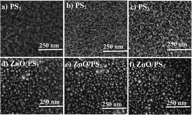 |
| | Fig. 1 FESEM images of PS and ZnO/PS. | |
AFM 3D images are presented in ESI 1.† AFM analysis clearly shows that the surface roughness is increasing in the order of PS1 < PS2 < PS3 (Fig. 2). This clearly indicates that the roughness of the porous silicon increases with silicon etching time. In contradiction, the surface roughnesses of ZnO/PS1, ZnO/PS2 and ZnO/PS3 are the same as each other. In addition, the surface roughness of ZnO/PS is decreased compared to the roughness of porous silicon.
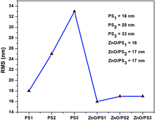 |
| | Fig. 2 RMS values of PS and ZnO/PS. | |
ESI 2† shows the XRD patterns of PS3 and ZnO/PS3. The XRD pattern of PS3 confirms the presence of the characteristic plane (400) of the silicon substrate with very high intensity. A very small intensity peak also evolved for the (330) plane which indicates the presence of a very small amount of polycrystalline silicon. The XRD pattern of ZnO coated nano-porous silicon shows the (100), (002), (101) and (110) planes observed at a 2θ of 31.8°, 34.4°, 36° and 56.5° respectively. These planes are related to hexagonal structured wurtzite zinc oxide crystal. The strong and sharp reflections of the (100) and (002) planes indicate that the ZnO coatings on porous silicon are well crystalized.
A survey XPS spectrum of ZnO/PS (ESI 3†) indicates the presence of several peaks which are presented in ESI 4.† A fluorine peak evolved from the porous silicon substrate and the presence of a carbon peak is due to the incomplete oxidation of diethyl zinc (DEZ) or contaminations. O (KLL) and Zn (KLL) represent the Auger series of oxygen and zinc respectively. The corresponding Auger parameters of O (KLL) and Zn (KLL) are 1039 eV and 2014.4 eV respectively. A high resolution zinc spectrum (ESI 5†) shows two peaks at 1021.1 eV which represents the Zn 2P3/2 state and at 1044.0 eV which represents the Zn 2P1/2 state. A high intensity peak is observed at 1021.1 eV for the Zn 2P3/2 core level which indicates that Zn species are in a completely oxidized state (Zn2+). The deconvoluted O1s core level spectrum (ESI 6†) shows two peaks at 529.9 eV which represents hexagonal wurtzite structured Zn–O species and 531.9 eV which represents Zn–OH species. The band gap energy (Eg) of ZnO is derived from the energy difference between an elastic peak (E O1s) and the onset of inelastic loss (Eloss) (ESI 7†). Therefore, the calculated band gap energy of ZnO is 3.8 eV which is close to the band gap energy of ZnO of 3.37 eV. The deconvoluted C 1s shows three peaks at 284.6 eV, 287.4 eV and 290.1 eV which indicate the presence of C–C or C–H, C–OH and C–OOH species respectively (ESI 8†). These species are evolved due to ALD precursors which are not completely desorbed during the ALD purge process.
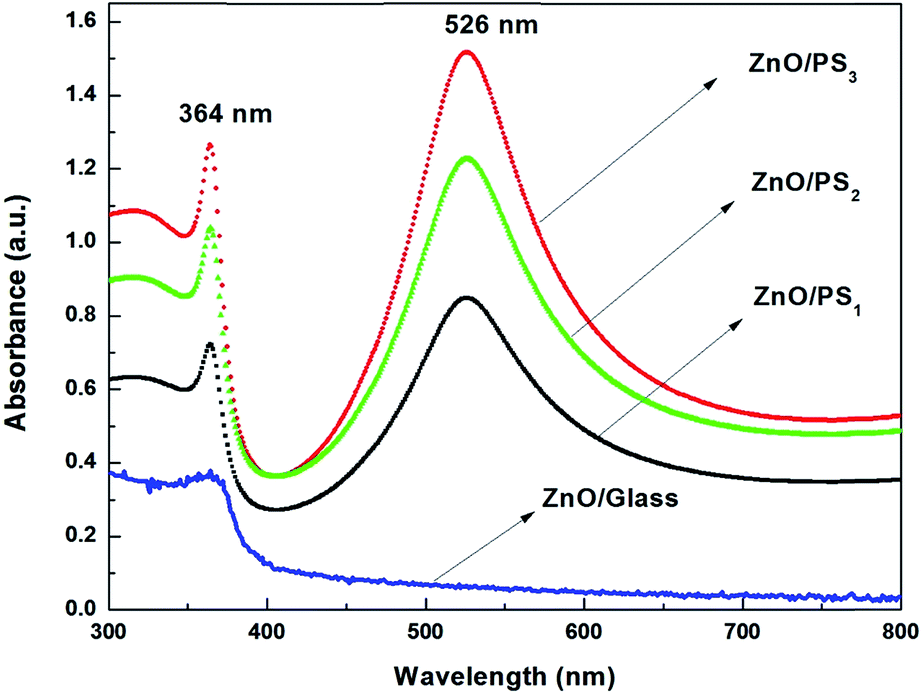
ESI 9† shows the DRS UV-Vis absorbance spectra of pure silicon and porous silicon. It is identified that the absorbance is increased by increasing the etching time of silicon. Fig. 3 shows the DRS UV-Vis absorbance spectra of ZnO coated porous silicon. The absorbance spectrum of ZnO coated glass shows the UV absorbance characteristic peak of ZnO at 364 nm. In contradiction, ZnO/PS exhibits a very strong absorbance peak in the visible light region around 526 nm. The absorbance onset of ZnO/PS is around 500 nm which indicates that the ZnO/PS acts as an efficient solar absorber. In addition, the absorbance percentage of ZnO/PS3 is higher than that of ZnO/PS1 and ZnO/PS2. This clearly indicates that the visible light absorbance of ZnO/porous silicon depends on the etching time of porous silicon. The visible light absorbance unit percentage of ZnO/PS increases continuously with increasing etching time as evidenced from the DRS UV-Vis absorbance spectrum.
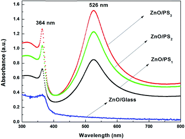 |
| | Fig. 3 DRS UV-Vis absorbance spectra of ZnO and ZnO/PS. | |
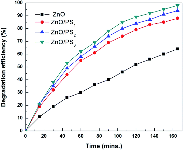
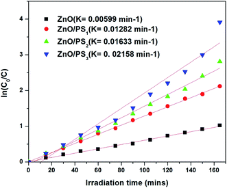
Fig. 4 shows the solar photocatalytic activity of ZnO/PS. ZnO/PS exhibited enhanced photocatalytic activity compared to ZnO coated glass. The linear relationship of ln(C0/C) versus time shows that the photocatalytic activity on the MB dye followed a pseudo first order expression,
where,
k is the apparent first order rate constant (
Fig. 5). The calculated reaction rate constants of ZnO, ZnO/PS
1, ZnO/PS
2 and ZnO/PS
3 are 0.354 s
−1 and 0.768 s
−1, 0.996 s
−1 and 1.29 s
−1 respectively. This clearly indicates that the reaction rate constant of ZnO/PS
3 is higher compared to others. The enhanced solar photocatalytic activity of ZnO/PS is attributed to the strongest visible light absorption around 526 nm as evidenced from the absorbance spectrum. Particularly, ZnO/PS
3 shows higher solar photocatalytic activity than ZnO/PS
1 and ZnO/PS
2 because the overall solar absorbance of ZnO/PS
3 is higher than that of ZnO/PS
1 and ZnO/PS
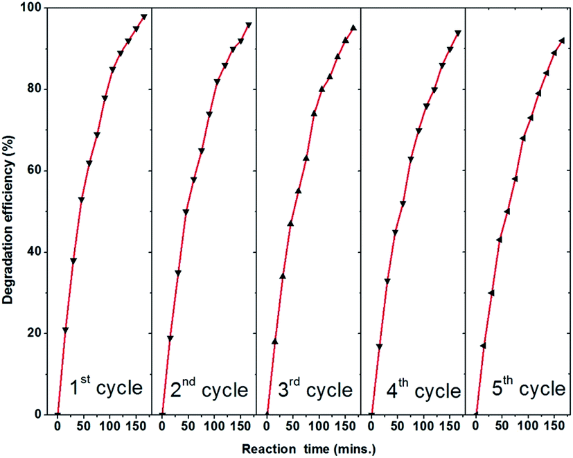
2. This clearly indicates that the photocatalytic activity of ZnO/PS increases continuously by increasing the etching time of porous silicon. The effective injection of the photogenerated electrons of porous silicon into ZnO is another factor that enhances solar photocatalytic activity even if porous silicon is not participating in any redox reactions. Moreover, the recyclability of ZnO/PS
3 is investigated and plotted in
Fig. 6. This shows a very small variation in the photocatalytic efficiency of ZnO/PS
3 after the 5
th cycle.
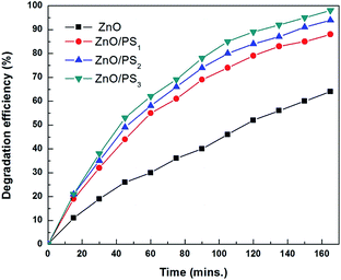 |
| | Fig. 4 Solar photocatalytic activity of ZnO and ZnO/PS. | |
 |
| | Fig. 5 Photoelectrocatalytic activity of ZnO/PS3. | |
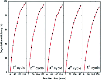 |
| | Fig. 6 Recycle performance of ZnO/PS3. | |
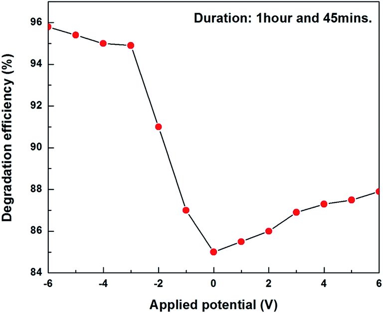
ZnO/PS3 was used for photoelectrocatalytic activity studies out of ZnO/PS1, ZnO/PS2 and ZnO/PS3, due to its superior solar photocatalytic activity. Fig. 7 shows the photoelectrocatalytic activity of ZnO/PS. It was identified that negative biased ZnO/PS exhibited higher solar photocatalytic activity compared to positive and unbiased ZnO/PS. The enhanced photoelectrocatalytic activity of ZnO/PS is attributed to the effective charge carrier separation by driving photogenerated holes via an external circuit to the counter electrode during negative bias.
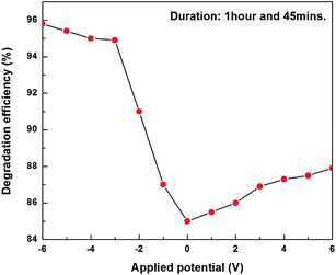 |
| | Fig. 7 Photoelectrocatalytic activity of ZnO/PS3. | |
When the applied positive potential of ZnO/PS is higher than the critical potential, called the flat band potential, the band bending of an n type semiconductor (ZnO) occurs with the electrolyte. The energy difference between the Fermi levels of the electrolyte and semiconductor determines the degree of band-bending within ZnO. As a result of band bending in this Schottky junction, the conduction band electrons of ZnO flow via an external circuit to the platinum counter electrode where reduction reactions take place and the valance band holes of ZnO enrich on the surface of the ZnO electrode where oxidation reactions take place. At the same time, the photogenerated electrons of porous silicon also flow to the counter electrode directly or via ZnO which leads to efficient degradation reactions (Fig. 8). In contradiction, the photogenerated holes cannot flow and enrich on the surface of ZnO due to the inappropriate band positions between ZnO and porous silicon which decreases the degradation reactions. It is worth noting that enhanced catalytic activity can be achieved in photo-electrocatalysis and faster electron–hole separation can be achieved with greater band-bending or space charge layer (SCL).
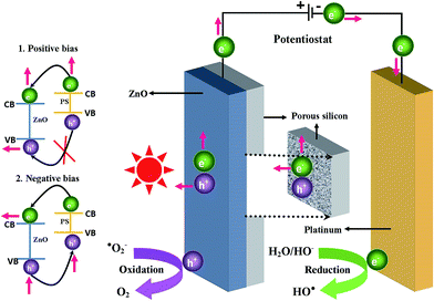 |
| | Fig. 8 Schematic diagram of electrochemical cell and bias notation of ZnO/PS. | |
Negative biased ZnO/PS3 shows enhanced photocatalytic activity compared to positive biased and unbiased ZnO/PS. The reason for such an enhanced photocatalytic activity is the effective injection of photogenerated electrons from porous silicon. When we look into the band structure of porous silicon, the potential of the conduction band position is lower than the potential of the conduction band position of the ZnO.21 The energy of the valance band position of porous silicon is also lower than the band position of ZnO. When we apply positive bias, the photogenerated holes in porous silicon cannot inject into the ZnO layer due to inappropriate band positions between porous silicon and ZnO. The photogenerated electrons from the ZnO can only move to the porous silicon and then move to the platinum counter electrode. Therefore, porous silicon contributes only photogenerated electrons for the dye degradation when ZnO/PS is connected to a positive potential. In contradiction, the photogenerated electrons in negative biased porous silicon can easily move to the ZnO layer due to appropriate band positions between porous silicon and ZnO. Moreover, the photogenerated holes from the ZnO can easily move to the porous silicon and then move to the counter electrode where oxidation reactions take place.20 As a result, the holes are depleted and electrons are enriched on the surface of the ZnO layer. Therefore, the photogenerated charge carriers of both porous silicon and ZnO are completely utilized for redox reactions when negative bias is applied to the ZnO/PS.
4. Conclusions
ZnO coated nanoporous silicon was prepared by a combined technique of stain etching and ALD. The surface roughness of the nanoporous silicon increases continuously with the etching time of silicon, which could be a consequence of an increased active surface area. ZnO coated nanoporous silicon exhibited very strong visible light absorbance around 526 nm. The photocatalytic and photoelectrocatalytic activity of ZnO/PS is investigated by degrading aqueous MB dye solution. The result shows that ZnO/PS exhibited higher photocatalytic activity compared to an ordinary ZnO coating. The enhanced photocatalytic activity is attributed to the visible light absorption of ZnO/PS. Even though porous silicon is not participating in any redox reactions, it injects photogenerated electrons effectively into the ZnO layer which enhances the photocatalytic activity. It is identified that both negative and positive biased ZnO/PS exhibited higher photocatalytic activity compared to unbiased ZnO/PS. Particularly, negative biased ZnO/PS shows higher photocatalytic activity compared to unbiased and positive biased ZnO/PS. In addition, the recyclability study of ZnO/PS shows that the variation in photocatalytic efficiency is negligible after the 5th run.
Acknowledgements
S. S. thanks CIMO, Finland for Finnish Government Scholarship Pool program. This research has been supported by the project CZ.1.05/2.1.00/03.0086 funded by European Regional Development Fund and project LO1411 (NPU I) funded by Ministry of Education Youth and Sports of Czech Republic.
References
- J. Mu, C. Shao, Z. Guo, Z. Zhang, M. Zhang, P. Zhang, B. Chen and Y. Li, ACS Appl. Mater. Interfaces, 2011, 3, 590–596 CAS.
- R. Mohan, K. Krishnamoorthy and S. J. Kim, Solid State Commun., 2012, 152, 375–380 CrossRef CAS.
- C. Xu, L. Cao, G. Su, W. Liu, X. Qu and Y. Yu, J. Alloys Compd., 2010, 497, 373–376 CrossRef CAS.
- H. Bouzid, M. Faisal, F. A. Harraz, S. A. Al-Sayari and A. A. Ismail, Catal. Today, 2014, 252, 20–26 CrossRef.
- M. Zheng and J. Wu, Appl. Surf. Sci., 2009, 255, 5656–5661 CrossRef CAS.
- Y. Sun, T. He, H. Guo, T. Zhang, W. Wang and Z. Dai, Appl. Surf. Sci., 2010, 257, 1125–1128 CrossRef CAS.
- M. H. Habibi and M. H. Rahmati, Spectrochim. Acta, Part A, 2015, 137, 160–164 CrossRef CAS PubMed.
- R. Saravanan, V. K. Gupta, E. Mosquera and F. Gracia, J. Mol. Liq., 2014, 198, 409–412 CrossRef CAS.
- S. M. Lam, J. C. Sin, A. Z. Abdullah and A. R. Mohamed, J. Colloid Interface Sci., 2015, 450, 34–44 CrossRef CAS PubMed.
- M. Fan, C. Yang, W. Pu and J. D. Zhang, Mater. Sci. Semicond. Process., 2014, 17, 104–109 CrossRef CAS.
- P. Jongnavakit, P. Amornpitoksuk, S. Suwanboon and N. dieg, Appl. Surf. Sci., 2012, 258, 8192–8198 CrossRef CAS.
- L. Ma, S. Ma, H. Chen, X. Ai and X. Huang, Appl. Surf. Sci., 2011, 257, 10036–10041 CrossRef CAS.
- P. S. Maydannik, A. Plyushch, M. Sillanpää and D. C. Cameron, J. Vac. Sci. Technol., A, 2015, 33, 3 Search PubMed.
- V. Pore, M. Heikkilä, M. Ritala, M. Leskelä and S. Areva, J. Photochem. Photobiol., A, 2006, 177, 68–75 CrossRef CAS.
- R. L. Puurunen, J. Appl. Phys., 2005, 97, 121301 CrossRef.
- M. Leskelä and M. Ritala, Thin Solid Films, 2002, 409, 138–146 CrossRef.
- S. M. George, Chem. Rev., 2010, 110, 111–131 CrossRef CAS PubMed.
- M. Fan, C. Yang, W. Pu and J. Zhang, Mater. Sci. Semicond. Process., 2014, 17, 104–109 CrossRef CAS.
- Z. Li, F. Gao, W. Kang, Z. Chen, M. Wu, L. Wang and D. Pan, Mater. Lett., 2013, 97, 52–55 CrossRef CAS.
- Y. S. Sakhare, S. V. Bhoraskar, V. L. Mathe and A. U. Ubale, Mater. Res. Bull., 2014, 59, 205–213 CrossRef CAS.
- V. E. Drozd, V. V. Titov, I. A. Kasatkin, L. L. Basov, A. A. Lisachenko, O. L. Stroyuk and S. Y. Kuchmiy, Thin Solid Films, 2014, 573, 128–133 CrossRef CAS.
Footnote |
| † Electronic supplementary information (ESI) available. See DOI: 10.1039/c6ra01655c |
|
| This journal is © The Royal Society of Chemistry 2016 |
Click here to see how this site uses Cookies. View our privacy policy here. 
 Open Access Article
 This Open Access Article is licensed under a Creative Commons Attribution-Non Commercial 3.0 Unported Licence