
Epitaxial growth and nanoscale electrical properties of Ce2Ti2O7 thin films†
Alexandre Bayart,
ZhenMian Shao,
Anthony Ferri,
Pascal Roussel,
Rachel Desfeux and
Sébastien Saitzek*
Faculté des Sciences Jean Perrin, Univ. Artois, CNRS, Centrale Lille, ENSCL, Univ. Lille, UMR 8181, Unité de Catalyse et Chimie du Solide (UCCS), F-62300 Lens, France. E-mail: sebastien.saitzek@univ-artois.fr; Fax: +33 321791755; Tel: +33 321791732
First published on 22nd March 2016
Abstract
(00l) epitaxial Ce2Ti2O7 thin films with a layered perovskite/monoclinic structure were grown on (110)-oriented Nb-doped SrTiO3 substrates via pulsed laser deposition and a sol–gel method associated with spin-coating. Using the sol–gel method, the Ce2Ti2O7 films were obtained by annealing at 950 °C under a reductive Ar/H2 atmosphere. Employing the pulsed laser deposition technique, they were directly grown under vacuum (10−6 mbar) with a controlled re-oxidation during the cooling step. The pole figure measurements provide the in-plane crystallographic relationships between the film and substrate: [001]SrTiO3//[100]Ce2Ti2O7 and [1−10]SrTiO3//[010]Ce2Ti2O7. Piezoresponse force microscopy measurements highlight the local ferroelectric character of the films synthetized. The switching capability was more reliable for the film grown via pulsed laser deposition, which was explained by the lower mosaic spread. Higher local conductivity was also detected using conductive-atomic force microscopy of the physically deposited film and was attributed to its lower thickness. Such epitaxially deposited functional oxides may be considered as promising candidates for integration into advanced electronic devices.
1. Introduction
For many years, the search for lead-free ferroelectric materials has experienced real developments because of the increasing environmental constraints for manufacturers of electronic devices. To meet these new standards, manufacturers must use active materials with low power consumption and integrate them into the industrial process with eco-parameters, which include substituting harmful materials to human health and the environment such as lead-based compounds. For this reason and despite their better efficiency (high remnant polarization and low coercive field), traditional lead-based ferroelectric materials, e.g. PbZrTiO3 or Pb(MgNb)O3–PbTiO3,1 are gradually being replaced for the benefit of new lead-free compounds. The economic potential of these lead-free ferroelectric materials becomes significant because they can be found in many fields of continuous development such as mobile telephony,2,3 micro-electromechanical systems (MEMS)4 or data storage.5,6Among the known lead-free ferroelectric compounds, the Ln2Ti2O7 family, with Ln = La to Nd bearing a layered-perovskite structure, has been studied especially for the ferroelectric properties and for its use in extreme environments due to its high Curie temperature (Tc ∼ 1500 °C).7–10 In addition, these compounds are known for the photo-catalytic properties (water splitting),11,12 the photoluminescent properties when doped with rare earth13,14 or even for their great ability for the realization of immobilization matrices of highly active radio-nuclides from nuclear waste.15
The synthesis of Ln2Ti2O7 (with Ln = La, Pr, Nd, Sm and Gd) thin films has already been successfully performed using different techniques, e.g. sol–gel (SG) routes associated with spin-coating technique,16–19 molecular beam epitaxy (MBE),20 and pulsed laser deposition (PLD).21–23
However, among this family, studies on the Ce2Ti2O7 (CeTO) compound are very scarce because it is very difficult to stabilize the +III valence state of cerium. In the literature, there are three cerium titanates involving mainly the Ce3+ cation in the Ce–Ti–O system: Ce2TiO5, Ce2Ti2O7 and Ce4Ti9O24.24 The stabilization of the CeTO phase requires a good stoichiometric ratio of 1![[thin space (1/6-em)]](https://www.rsc.org/images/entities/char_2009.gif) :1 (Ce:Ti) during the synthesis process. Ln2Ti2O7 compounds adopt a layered-perovskite structure for large Ln3+ ionic radii (Ln = La to Nd), whereas they prefer a pyrochlore type for small Ln3+ ionic radii (Ln = Sm to Lu). In general, the stability of these structures depends on the ratio between the cations radii of Ln3+ and Ti4+. Thus, for r(Ln3+)/r(Ti4+) included in the range of 1.46–1.78, the formed compound will adopt a pyrochlore-like structure. For ratios higher than 1.78, the layered-perovskite type is preferred. However, studies have shown that this limit can be extended by epitaxial strain: Sm2-/Eu2-/Gd2Ti2O7 compounds may have a layered-perovskite structure.17,25
:1 (Ce:Ti) during the synthesis process. Ln2Ti2O7 compounds adopt a layered-perovskite structure for large Ln3+ ionic radii (Ln = La to Nd), whereas they prefer a pyrochlore type for small Ln3+ ionic radii (Ln = Sm to Lu). In general, the stability of these structures depends on the ratio between the cations radii of Ln3+ and Ti4+. Thus, for r(Ln3+)/r(Ti4+) included in the range of 1.46–1.78, the formed compound will adopt a pyrochlore-like structure. For ratios higher than 1.78, the layered-perovskite type is preferred. However, studies have shown that this limit can be extended by epitaxial strain: Sm2-/Eu2-/Gd2Ti2O7 compounds may have a layered-perovskite structure.17,25
CeTO layered-perovskite is formed by Ce3+ and Ti4+ ions in eight- and six-fold coordination, respectively. The ionic radii of Ce3+ and Ti4+ in these coordinate sites are 1.143 and 0.605 Å, respectively.26 These values yield a ratio of 1.89, which is within the tolerated range for the layered-perovskite structure. This structure is non-centrosymmetric and thus may present piezoelectric and ferroelectric properties.
To the best of our knowledge, only one study performed by Kim et al.27 was focused on the growth of ferroelectric CeTO thin film. The film was polycrystalline and deposited on a Y2O3/Si substrate via chemical solution deposition. In this study, the authors show that the film has a similar structure to La2Ti2O7. The remnant polarization (Pr) and coercive field (Ec) values determined from the Metal–Ferroelectric–Metal (MFM) stacking structure were 4.16 μC cm−2 and 126.8 kV cm−1, respectively.27 More recently, the piezoelectric activity was measured by Z. Gao et al. in ceramic with a layered-perovskite structure at a value of 0.4 ± 0.2 pC/N.28 The Curie temperature of Ce2Ti2O7 was also estimated about 1073 °C. This temperature is lower when compared to La2Ti2O7, Pr2Ti2O7 and Nd2Ti2O7 compounds, but remains a very high value beside other lead-free ferroelectric materials. Furthermore, at the image of La2Ti2O7, which is a highly resistant oxide to the ion-beam irradiation,29,30 CeTO can be considered as a promising advanced functional materials for the realization of nanostructures or for use in extreme conditions such as high temperature, high pressure, or high stress conditions. The Ce2Ti2O7 compound can be employed in high performance engineering applications, e.g. aerospace, automotive, sensors, and electronic industries. Finally, it has also been shown that La2Ti2O7 oxide (isostructural to Ce2Ti2O7) may have multiferroic properties at room temperature when it is doped with transition metals such as Co, Fe, Mn, and Cr.31 This opens the way for promising uses of the Ln2Ti2O7 family compounds in different fields.
In the present study, we present two synthesis routes to obtain an epitaxial CeTO thin film on (110)-oriented SrTiO3 (STO) substrate. The first method is derived from the wet chemistry, wherein we use a sol–gel (SG) route associated with the spin-coating technique. The second method is a physical deposition method employing the pulsed laser deposition (PLD) technique.
This study presents, for the first time, the epitaxial growth of CeTO thin films via two techniques of deposition. The micro-structural properties obtained using high resolution X-ray diffraction (HR-XRD) and the electrical properties at the nano-scale level via piezo-force microscopy (PFM) and conductive atomic force microscopy (c-AFM) were investigated to (i) unambiguously highlight the ferroelectric properties of the films, with the first images of the switched ferroelectric domains and (ii) conduct a comparative study involving the electronic properties and microstructures of the materials.
2. Experimental section
First, a sol–gel process was used to synthesize CeTO thin films. Titanium iso-propoxide (Ti(OCH(CH3)2)4, 98.0%, Acros Organics), 2-methoxyethanol (C3H8O2, 99.0%, Sigma Aldrich), 2,4-pentadione (C5H8O2, 99+%, Sigma Aldrich) and cerium(III) nitrate hexahydrate (Ce(NO3)3·6H2O, 99.9%, Strem Chemicals) were used as starting materials. The synthesis is carried out in two stages. A first solution (A) was obtained by mixing the solvents: 2-methoxyethanol and 2,4-pentadione in a volume ratio of 6.5/1.5. After two hours of stirring, titanium iso-propoxide was added to this solution (to obtain a concentration of 0.4 mol L−1). Then, an additional stirring of 2 hours at ambient temperature was realized. In parallel, a second solution (B) was achieved by mixing cerium nitrate in 2-methoxyethanol (the concentration of Ce3+ was fixed at 0.4 mol L−1). Then, this solution was mixed for 2 hours at 50 °C. Finally, solutions A and B were mixed (with volume ratio 1:1) and stirred during 3 hours to form the gel. The flowchart of the synthesis procedure was already detailed in our previous studies.16,25 CeTO gels were spin coated at 3000 rpm for 60 s onto (110)-oriented STO single crystal substrates (Crystal GmbH, Germany). A drying step was performed at 250 °C for 15 minutes after each deposition. Then, the coated films were annealed at 950 °C in an Ar/H2 (3%) reductive mixture for 1 hour. The typical film thickness, as measured by ellipsometry, was approximately 150 nm.
Second, a PLD technique was used to synthesize CeTO films on (110)-oriented STO single crystal substrates. All substrates were first ultrasonically cleaned in acetone and then in ethanol for 5 minutes. Each substrate was attached to a heater plate using silver paste. The Ce2Ti2O7 target cannot be directly obtained with the solid–state reaction route. Indeed, obtaining the Ce3+ cation requires the process to be carried out under a reductive atmosphere. However, in this present study, we investigated whether it was possible to reduce the Ce(IV) in Ce(III) via a reactive pulsed laser deposition under vacuum (10−6 mbar). To constitute the target, cerium oxide (Strem Chemicals, 99.9%) and titanium oxide (Strem Chemicals, 99.9%) were used as starting materials. These oxides were mixed finely (using ball-milling – 350 rpm/4 h) at an atomic ratio of 1:1. Finally, a target of 1 in. in diameter was prepared after uniaxial pressing and sintering at 1200 °C for 6 h. As expected, the X-ray patterns realized on the pellet show only the coexistence of X-ray diffraction peaks attributed to the CeO2 and TiO2 oxides.
Deposition was carried out using a KrF excimer laser operating at a wavelength of 248 nm (Compex Pro 102). The deposition rate and the fluence were 3 Hz and 2 J cm−2, respectively, while the target–substrate distance was adjusted to d = 4.5 cm. All films were deposited on SrTiO3 substrates heated to 900 °C and 4000 laser pulses were used.
To obtain Ce2Ti2O7 thin films, a slight oxidation under static oxygen pressure (10 mbar) during the cooling step was performed. This last step was necessary. Indeed, if the cooling was carried out under vacuum (10−6 mbar as for the deposition step), a two-phase mixture (CeTiO3+δ/γ-Ce2Ti2O7) was obtained. The thickness of the Ce2Ti2O7 thin films synthetized was about 75 nm.23
The structural characterization of the films was performed using a Rigaku SmartLab HR X-ray diffractometer equipped with a 9 kW rotating anode X-ray generator (λKα1 = 1.54059 nm). The X-ray beam was made parallel with a Göbel mirror and monochromatized with a double Ge (220) monochromator. In this study, all the (θ–θ) scans were performed in the range of 10–80°, with a step size of 0.02° and with a speed of 1° min−1. This configuration was also used to achieve rocking-curves and ϕ-scans measurements.
The surface morphology of the films was characterized using the AFM technique in alternative contact (or Tapping™) mode. Piezo-/ferroelectric properties were locally probed using the piezoresponse mode of AFM in air at room temperature. Pt/Ir-coated silicon tips and stiff cantilevers (k ∼ 5 N m−1) were used as the conductive probe in order to enhance the electromechanical response and reduce the electrostatic interactions during PFM experiments.32 The switching behavior and piezoelectric activity of the domains were studied at the nanoscale by both imaging and spectroscopic PFM measurements. Local conductivity variations were detected by the ORCA conductive-AFM technique (MFP-3D, Asylum Research) in air. Ti/Ir-coated silicon grounded tips and cantilevers with a stiffness of ∼2 N m−1 were used. Current maps were obtained by applying a bias voltage of −3 V between the grounded tip and the conductive substrate. All ORCA experiments were performed the same day without changing the probing tip.
3. Results and discussion
Fig. 1a presents the XRD patterns of the CeTO thin films with a layered-perovskite stucture and deposited onto (110)-oriented STO substrates. Under the optimum growth conditions described in the experimental section, CeTO adopts the expected monoclinic (P21) structure with (00l) orientations for the two synthetic routes. However, differences appear in the XRD patterns according to the synthesis route used. Indeed, a single phase was observed for the SG method, while additional peaks were observed for the PLD technique. An additional peak attributed to ceria was observed at 47.50° (JCPDS 75-0390) and two peaks marked with a star “*” were attributed to the CeTi2O6 phase with a (hh0) orientation (JCPDS 12-0477). | ||
| Fig. 1 (a) The XRD patterns of Ce2Ti2O7 grown on a (110)-oriented SrTiO3 substrate via PLD or sol–gel methods. (b) Rocking curves recorded for the (004) reflection of Ce2Ti2O7. | ||
The presence of ceria can be explained by the nature of the target used consisting of a stoichiometric mixture of CeO2/TiO2. In addition, the (002) orientation of ceria without other peaks suggests an epitaxial growth as CeTO. To check, we performed a pole figure at 2θ = 33.08° corresponding to the {200} reflection of CeO2. The results are given in Fig. 2a for both the observed and simulated ones. The analysis was performed by a visual comparison of the measured enhanced pole densities with the calculated spherical projections of STO, CeO2 and CeTO crystals, using the software STEREOPOLE.33 The different poles observed can be simulated considering a (200) oriented CeO2 film (red index) and (001) oriented CeTO film (green index) deposited on a (110)-oriented STO substrate (blue index). Because only punctual poles are observed one can conclude the epitaxial growth. The epitaxial relationships deduced from this pole figure are: [001]SrTiO3//[100]Ce2Ti2O7 and [1−10]SrTiO3//[010]Ce2Ti2O7; [100]SrTiO3//[011]CeO2 and [01−1]SrTiO3//[100]CeO2.
 | ||
| Fig. 2 (a) Pole figure obtained at 2θ = 33.08°, (b) pole figure obtained at 2θ = 47.48° for Ce2Ti2O7 thin film grown on a (110)-oriented SrTiO3 substrate via PLD. | ||
In the literature, it has been shown that the La2Ti2O7 structure (which is isostructural to CeTO) has a twinning.34 In the tabulated monoclinic unit cell used in our study, the twinning operation corresponds to a mirror plane perpendicular to the ![[c with combining right harpoon above (vector)]](https://www.rsc.org/images/entities/i_char_0063_20d1.gif) * direction giving two directions for the
* direction giving two directions for the ![[a with combining right harpoon above (vector)]](https://www.rsc.org/images/entities/i_char_0061_20d1.gif) *-axis (the angle between *twin1 and *twin2 is equal to 2(β-90°)). To observe the presence of twinning (i.e. the presence of two domains of CeTO in the thin film), we realized a pole figure at 2θ = 47.48° (Fig. 2b). This angle is chosen to observe the reflections of the substrate ({200} reflection of STO to 46.48°), CeO2 layer ({220} reflection to 47.48°) and CeTO layer (because there are intense reflections at 47.30°, 47.40°, 48.35°, and 48.55° corresponding to {223}, {224}, {025} and {215} reflections of the monoclinic structure, respectively). The different poles observed can be simulated considering a (022)-oriented CeO2 film (red index) and (001)-oriented CeTO film (green index) deposited on a (110)-oriented STO substrate (blue index). The (025) reflection of CeTO coincides with the {020} reflection of the substrate; the {223} and {224} reflections of CeTO coincides with the CeO2 reflections (these reflections are not indicated in the figure to avoid overlapping). However, we observe the presence of four peaks for the {215} reflection of CeTO wherein we should get two in a monoclinic symmetry with the P21 space group. The presence of these four peaks can be explained by the presence of twinning in the film structure. Therefore, we observe two domains indexed D1 and D2 in the pole figure. This result confirms the similar behavior of Ce2Ti2O7 and La2Ti2O7 structures.
*-axis (the angle between *twin1 and *twin2 is equal to 2(β-90°)). To observe the presence of twinning (i.e. the presence of two domains of CeTO in the thin film), we realized a pole figure at 2θ = 47.48° (Fig. 2b). This angle is chosen to observe the reflections of the substrate ({200} reflection of STO to 46.48°), CeO2 layer ({220} reflection to 47.48°) and CeTO layer (because there are intense reflections at 47.30°, 47.40°, 48.35°, and 48.55° corresponding to {223}, {224}, {025} and {215} reflections of the monoclinic structure, respectively). The different poles observed can be simulated considering a (022)-oriented CeO2 film (red index) and (001)-oriented CeTO film (green index) deposited on a (110)-oriented STO substrate (blue index). The (025) reflection of CeTO coincides with the {020} reflection of the substrate; the {223} and {224} reflections of CeTO coincides with the CeO2 reflections (these reflections are not indicated in the figure to avoid overlapping). However, we observe the presence of four peaks for the {215} reflection of CeTO wherein we should get two in a monoclinic symmetry with the P21 space group. The presence of these four peaks can be explained by the presence of twinning in the film structure. Therefore, we observe two domains indexed D1 and D2 in the pole figure. This result confirms the similar behavior of Ce2Ti2O7 and La2Ti2O7 structures.
In addition, we observe a higher crystallinity for films deposited via the PLD technique, as expected. This was confirmed by the rocking curves measurements shown in Fig. 1b, wherein the mosaic spread was also less important for the films synthesized via PLD (FWHM = 0.11°) compared to films deposited via the SG route associated with spin-coating (FWHM = 0.43°). Overall, the CeTO–PLD films exhibit better structural quality but possess an unwanted phase.
The (00l) orientation is not surprising if we take into account the good geometric arrangement between the perovskite (001)-planes and the substrate (110)-planes. Indeed, CeTO is isotypic to Ln2Ti2O7 (with Ln = La, Pr and Nd) and crystallizes in the monoclinic structure with a P21 space group. The lattice parameters are given by Preuss et al.: a = 7.776(6) Å, b = 5.515(4) Å, c = 12.999(6) Å and β = 98.36(5)°.24 Using these bibliographical lattice parameters for the CeTO bulk materials and considering a = 3.905 Å as the lattice parameter for the STO substrate, we can calculate the CeTO/STO lattice-substrate mismatches (δ, δ′) with the following equation:23
 | (1) |
The small values obtained confirm the good compatibility between the in-plane lattice parameters of the films and the substrate, thus explaining the growth of the films with -axis out-of-plane but with slight in-plane tensile strain. Considering previous study on La2Ti2O7, Pr2Ti2O7 and Nd2Ti2O7 thin films, the more ionic radius of the lanthanide decreases, the more the tensile strain becomes significant.35 The strain and the crystallite size can be determined using Williamson–Hall (W–H) analysis on the (00l) reflections:36
 | (2) |
 | ||
| Fig. 3 Williamson–Hall plots performed on the (00l) reflections of Ce2Ti2O7 grown on a (110)-oriented SrTiO3 substrate. | ||
For both techniques, we observe significant values for strain associated to the -axis. These values can be explained in particular by the adjustment of the structure on the substrate and/or anisotropic shape of the crystallites. The W–H method provides the average crystallites size in the perpendicular direction of the substrate plane. To check the eventual anisotropic shape, we used the AFM technique to obtain information on the grain's size on the surface of the thin film. This aspect will be discussed later in this section. There is also an influence between the crystallite size and micro-strain. When the crystallites size decreases, there is an increase in micro-strains.37,38 This explains the higher value for the micro-strain in thin films derived from the SG route wherein the crystallites sizes are smaller.
To study the influence of static cooling in the PLD technique, we synthesized thin films with cooling under 10−6 mbar (unlike the previously realized under 10 mbar of O2). For the (110)-oriented STO substrate, two phases were observed (Fig. 4). The first was CeTiO3+δ with the existence of peaks very close to the ones of the substrate. This phase can be indexed with the (200) or (020) orientations. Indeed, CeTiO3 crystallizes in an orthorhombic structure (space group Pbnm) whose lattice parameters are: a = 5.570 Å, b = 5.584 Å, c = 7.865 Å.39 The CeTiO3 can comfortably fit on the (110) plane of the STO with the -axis or ![[b with combining right harpoon above (vector)]](https://www.rsc.org/images/entities/i_char_0062_20d1.gif) -axis perpendicular to the substrate plane (Fig. 5a). Indeed, the a and b lattice parameters were close enough and both orientations were possible. To check the epitaxial growth, we have performed pole figures at 2θ = 31.88° (Fig. 5b), corresponding to the {112} reflection of CeTiO3 (lattice parameters of the bulk were used to determine this angle) and at 2θ = 46.42° (Fig. 5c), corresponding to the {002} reflection of STO. The epitaxial relationships deduced from these pole figures are: [002]SrTiO3//[002]CeTiO3 and [022]SrTiO3//[020]CeTiO3 or [200]CeTiO3.
-axis perpendicular to the substrate plane (Fig. 5a). Indeed, the a and b lattice parameters were close enough and both orientations were possible. To check the epitaxial growth, we have performed pole figures at 2θ = 31.88° (Fig. 5b), corresponding to the {112} reflection of CeTiO3 (lattice parameters of the bulk were used to determine this angle) and at 2θ = 46.42° (Fig. 5c), corresponding to the {002} reflection of STO. The epitaxial relationships deduced from these pole figures are: [002]SrTiO3//[002]CeTiO3 and [022]SrTiO3//[020]CeTiO3 or [200]CeTiO3.
 | ||
| Fig. 4 XRD patterns of CeTiO3+δ and γ-Ce2Ti2O7 thin films grown on (110) oriented SrTiO3 substrates via PLD. | ||
 | ||
| Fig. 5 (a) Schematic of the epitaxial relationships between the CeTiO3 film and the (110)-oriented STO substrate. (b) Pole figure obtained at 2θ = 31.88°. (c) Pole figure obtained at 2θ = 46.42°. The blue squares correspond to the calculated positions of CeTiO3, while the red squares correspond to the poles of the STO substrate. | ||
The second was Ce2Ti2O7 crystallizing in a γ phase (polymorphic phase of Ce2Ti2O7 different from the previously described ferroelectric phase) with (00l) orientation. This phase was first observed in the case of cerium dititanate, but has already been observed for Re2Ti2O7 in thin films (with Re = La, Nd, Sm, Gd, Dy and Y) by Havelia S. et al.22 According to their study, this phase has an Ammm space group (Laue group) that cannot present ferroelectric properties. This phase disappears after annealing at 950 °C under a vacuum at 10−6 mbar.
In conclusion, the CeTiO3+δ thin films can be also elaborated via PLD from the CeO2:TiO2 target under vacuum without necessarily requiring a reductive atmosphere. To continue this work, a study of the electrical properties vs. the O2 pressure (used during the cooling step) could be conducted. A correlation between the electrical measurements and the δ value will also be interesting to achieve because these thin films may find potential applications as conducting (Mott–Hubbard transition)40–42 or as ferromagnetic oxides39 for δ close to 0.
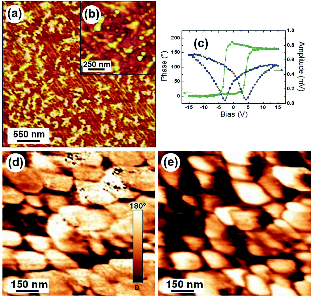
The surface topography of each synthesized film was investigated using tapping mode AFM, which offers a highly detailed drawing of the surface morphology. Fig. 6a and b depict the characteristic surface morphology of the CeTO film deposited onto a (110)-oriented STO via the SG method. We observe a dense granular-like surface comprising small elongated grains with widths of about 50 nm and lengths ranging from 80 to 120 nm, whereas the root mean square roughness (Rrms) value was measured to be around 4.4 nm over a 5 × 5 μm2 scan area. These results were comparable with those obtained for films belonging to the Ln2Ti2O7 family and previously deposited with the same SG technique.16,17 The AFM surface of the film deposited via PLD is shown in Fig. 7a and b. The surface is depicted by circular grains whose diameter was between 60 and 200 nm. The Rrms value was found to be about 2.9 nm over a 5 × 5 μm2 scan area. As a remark, the film prepared via PLD displays a better surface quality (more flat surface), whereas the grain size of CeTO was on average the largest. This later result correlates with the trend observed by the W–H plot.
 | ||
| Fig. 6 Local characterization of the Ce2Ti2O7 thin film deposited via a sol–gel method onto a (110)-oriented SrTiO3 substrate. (a), (b) AFM topography, (c) remnant phase and amplitude PFM loops, (d) out-of-plane and (e) in-plane PFM images recorded simultaneously. | ||
 | ||
| Fig. 7 Local characterization of the Ce2Ti2O7 thin film deposited via PLD onto a (110)-oriented SrTiO3 substrate. (a), (b) AFM topography, (c) remnant phase and amplitude PFM loops, (d) out-of-plane and (e) in-plane PFM images recorded simultaneously. | ||
Ce2Ti2O7 is known to present significant leakage current, which makes the measurement of the piezo-/ferroelectric properties at the macroscale difficult, as evidenced by the leaky P–E hysteresis loops observed.27 Consequently, the electrical properties were locally probed using PFM in this study. Remnant piezoresponse loops recorded using dual AC resonance tracking (DART) PFM43 over the surface of the CeTO film grown via SG are displayed in Fig. 6c. The phase loop reveals a ferroelectric-like behavior when considering the hysteretic response and the two opposite stable states. The electromechanical activity was demonstrated by the amplitude loop shown in the same figure, wherein a typical butterfly-shape was obtained. Both PFM loops were shifted along the voltage axis towards positive values, characteristic of the imprint behavior of the local switching and attributed to an internal built-in electric field, which exists in the film.44 In addition, asymmetry was observed in the tip vibration amplitude commonly due to the difference between the work functions of the tip and the conductive bottom layer.45 Out-of-plane (OP) and in-plane (IP) PFM imaging experiments performed over the surface reveal strong contrasted images, as observed in Fig. 6d and e, respectively. These various contrasts are the clear signature of the as-grown piezoelectric domains oriented along different directions included between the parallel and normal directions with respect to the film surface. Assuming the polarization vector is exclusively along the -axis for CeTO as reported for La2Ti2O7 and Nd2Ti2O7,35,36,46 these contrasts may be explained by the tensorial nature of the piezoelectric constants in such strained films and by the large mosaicity of the film inducing an out-of-plane component for the PFM signal, which can be observed in the OP-PFM images.35 The ferroelectric properties of CeTO thin films were also highlighted by poling experiments (see ESI Fig. S1†).
Piezoloops measured on CeTO/(110)-STO grown via PLD with a similar conducting tip and driving AC voltage (1.5 V) are shown in Fig. 7c. Both phase and amplitude loops were obtained, confirming the piezo-/ferroelectric nature of the film (the ferroelectric properties of the CeTO thin films were also confirmed by poling experiments shown in the ESI Fig. S1†). The more square shape for the phase loop associated to the well symmetric butterfly loop may be attributed to the better crystallinity of the ferroelectric CeTO crystallites, which leads to a more reliable switching capability. The OP- and IP-PFM images are depicted in Fig. 7d and e, respectively; wherein several contrasts can be observed. These contrasted regions represent the as-grown piezoelectric domains, as previously observed for the CeTO layer synthesized via an SG method. However, a significant difference was obtained in terms of the lateral domain size, because much larger domains are observed for the film deposited via the physical method, which was directly correlated with the grains lateral size. It can be noted that no correlation was obtained between the topography and the piezoelectric domains map (see ESI Fig. S2†).
Then, the local current was locally probed using the ORCA c-AFM technique over the surface of each film to estimate potential current leakages commonly observed at the macroscale for the Ln2Ti2O7 family. Fig. 8b and d display the nanoscale conductivity variations measured on the CeTO layers grown via the SG and PLD methods, respectively, with the simultaneously recorded topographies (Fig. 8a and c). No significant current signal was detected for the SG film, while the local current reaches −25 pA for the PLD sample, as evidenced by the red (dark) contrasts and the corresponding scale bar. The leakage currents were observed with an inhomogeneous distribution over the scanned surface, i.e., no obvious correlation was obtained between the topography and the current map, indicating both grains and grain boundaries do not represent a preferential electrical conducting channel. In addition, this local conductivity was not observed at the specific location of the potential ferroelectric domain walls as in the case of BiFeO3 or La-doped BiFeO3 thin films for example, because the lateral size of the detected current signal was relatively large.47,48 Two main reasons can explain such differences in the local conduction properties for both films: (i) the film deposited using the physical method was thinner than the chemically deposited film (75 vs. 150 nm, respectively). For such a lower thickness, the possibility of an electron crossing the height barrier was higher, inducing an increase in the leakage current.49 (ii) Two different routes are used for film growth. Naturally, dissimilarities inherent in the way employed such as the density of oxygen vacancies50 or the proportion of the crystal growth defects can induce conductivity variations.51 We have also to keep in mind that for the film elaborated via the PLD technique, parasitic phases are present and can induce an increase in defects leading to an increase in the conductivity, as observed.
 | ||
| Fig. 8 Local conductivity measured over the surface of the Ce2Ti2O7 layers grown via sol–gel and PLD methods. (a) AFM topography and (b) the corresponding ORCA current recorded over the surface of the Ce2Ti2O7 thin film grown via sol–gel. (c) AFM topography and (d) the corresponding ORCA current recorded over the surface of the Ce2Ti2O7 thin film grown via PLD. The scan area for all images is 1 × 1 μm2. Scale bars for the AFM and ORCA images are similar for both films. | ||
Moreover, despite the discrepancies observed, the low current values measured (∼pA) in these CeTO thin films may allow their possible integration in micro-electronic devices as an active ferroelectric material.
4. Conclusions
The epitaxial growth of Ce2Ti2O7 thin films on (110)-oriented SrTiO3 substrates was demonstrated using two techniques: pulsed laser deposition and sol–gel associated with the spin-coating technique. The thin films have an (00l) orientation and are isostructural to monoclinic La2Ti2O7. The PLD technique obtains thin films with better crystallinity and lower mosaic spread compared to the SG route. Piezoelectric domain patterns and local hysteresis loops produced by AFM demonstrate unambiguously the ferroelectric properties of the films on the nanoscale, with a more reliable switching capability observed for the PLD films. For the later films, the detection of local conductivity achieved by c-AFM reveals higher leakage currents probably due to both the lower thickness and the synthesis route compared to the chemically deposited film. Minimizing leakage currents is a key criterion for use in the field of micro/nano-electronics of these materials and for the applications such as ferroelectric random access memory or micro-electromechanical systems.Acknowledgements
Chevreul Institute (FR 2638), “Ministère de l'Enseignement Supérieur et de la Recherche”, “Région Nord Pas-de-Calais”, “FEDER” and “C'Nano Nord-Ouest competence centre” are acknowledged for supporting and funding this study. The “Fonds Européen de Développement Régional (FEDER)”, “CNRS”, “Région Nord Pas-de-Calais” and “Ministère de l'Education Nationale de l'Enseignement Supérieur et de la Recherche” are acknowledged for funding the X-ray diffractometers. The “Région Nord-Pas de Calais” and the FEDER under the “Contrat de Plan État-Région (CPER)” project “Chemistry and Materials for a Sustainable Growth” are gratefully acknowledged for funding the MFP-3D microscope. The authors wish to acknowledge A. Da Costa and L. Maes for technical support.References
- Y. Saito, H. Takao, T. Tani, T. Nonoyama, K. Takatori, T. Homma, T. Nagaya and M. Nakamura, Nature, 2004, 432, 84–87 CrossRef CAS PubMed.
- K. Kim and Y. J. Song, Microelectron. Reliab., 2003, 43, 385–398 CrossRef CAS.
- B. Min, M. Choi, S. Oh, N. Chang, B. Jeon and K. Kim, Curr. Appl. Phys., 2004, 4, 1–7 CrossRef.
- M. Goel, Ceram. Int., 2004, 30, 1147–1154 CrossRef CAS.
- R. Ramesh, Thin film ferroelectric materials and devices, Kluwer, Boston, 1997 Search PubMed.
- J. F. Scott, F. D. Morrison, M. Miyake and P. Zubko, Ferroelectrics, 2006, 336, 237–245 CrossRef CAS.
- A. Sayir, S. C. Farmer and F. Dynys, Ceram. Trans., 2006, 179, 57–68 CAS.
- W. S. Kim, S.-M. Ha, J.-K. Yang and H.-H. Park, Ferroelectrics, 2002, 271, 333–339 CrossRef CAS.
- H. Yan, H. Ning, Y. Kan, P. Wang and M. J. Reece, J. Am. Ceram. Soc., 2009, 92, 2270–2275 CrossRef CAS.
- Z. P. Gao, H. X. Yan, H. P. Ning and M. J. Reece, Adv. Appl. Ceram., 2013, 112, 69–74 CrossRef CAS.
- M. Uno, A. Kosuga, M. Okui, K. Horisaka and S. Yamanaka, J. Alloys Compd., 2005, 400, 270–275 CrossRef CAS.
- B. Vijaya Kumar, R. Velchuri, G. Prasad, B. Sreedhar, K. Ravikumar and M. Vithal, Ceram. Int., 2010, 36, 1347–1355 CrossRef.
- Z. Shao, S. Saitzek, J.-F. Blach, A. Sayede, P. Roussel and R. Desfeux, Eur. J. Inorg. Chem., 2011, 2011, 3569–3576 CrossRef CAS.
- L. K. Joseph, K. R. Dayas, S. Damodar, B. Krishnan, K. Krishnankutty, V. P. N. Nampoori and P. Radhakrishnan, Spectrochim. Acta, Part A, 2008, 71, 1281–1285 CrossRef PubMed.
- Y. Zhang, V. Shutthanandan, R. Devanathan, S. Thevuthasan, D. E. McCready, J. Young, G. Balakrishnan, D. M. Paul and W. J. Weber, Nucl. Instrum. Methods Phys. Res., Sect. B, 2004, 218, 89–94 CrossRef CAS.
- Z. Shao, S. Saitzek, P. Roussel, M. Huvé, R. Desfeux, O. Mentré and F. Abraham, J. Cryst. Growth, 2009, 311, 4134–4141 CrossRef CAS.
- Z. Shao, S. Saitzek, P. Roussel and R. Desfeux, J. Mater. Chem., 2012, 22, 24894–24901 RSC.
- A. V. Prasadarao, U. Selvaraj, S. Komarneni and A. S. Bhalla, J. Mater. Res., 1992, 7, 2859–2863 CrossRef CAS.
- Z. Shao, S. Saitzek, P. Roussel, A. Ferri, É. Bruyer, A. Sayede, M. Rguiti, O. Mentré and R. Desfeux, Adv. Eng. Mater., 2011, 13, 961–969 CrossRef CAS.
- J. Fompeyrine, J. W. Seo and J.-P. Locquet, J. Eur. Ceram. Soc., 1999, 19, 1493–1496 CrossRef CAS.
- S. Havelia, S. Wang, K. R. Balasubramaniam and P. A. Salvador, J. Solid State Chem., 2009, 182, 1603–1610 CrossRef CAS.
- S. Havelia, S. Wang, K. R. Balasubramaniam and P. A. Salvador, Cryst. Growth Des., 2009, 9, 4546–4554 CAS.
- A. Bayart, S. Saitzek, M.-H. Chambrier, Z. Shao, A. Ferri, M. Huvé, R. Pouhet, A. Tebano, P. Roussel and R. Desfeux, CrystEngComm, 2013, 15, 4341–4350 RSC.
- A. Preuss and R. Gruehn, J. Solid State Chem., 1994, 110, 363–369 CrossRef CAS.
- Z. Shao, S. Saitzek, A. Ferri, M. Rguiti, L. Dupont, P. Roussel and R. Desfeux, J. Mater. Chem., 2012, 22, 9806–9812 RSC.
- R. D. Shannon, Acta Crystallogr., Sect. A: Cryst. Phys., Diffr., Theor. Gen. Crystallogr., 1976, 32, 751–767 CrossRef.
- W. S. Kim, J.-K. Yang, C.-K. Lee, H.-S. Lee and H.-H. Park, Thin Solid Films, 2008, 517, 506–509 CrossRef CAS.
- Z. Gao, L. Liu, X. Han, X. Meng, L. Cao, G. Ma, Y. Liu, J. Yang, Q. Xie and H. He, J. Am. Ceram. Soc., 2015, 98(12), 3930–3934 CrossRef CAS.
- A. Ferri, S. Saitzek, Z. Shao, G. Declercq, J. Costecalde, D. Rémiens, D. Deresmes, D. Troadec and R. Desfeux, J. Am. Ceram. Soc., 2013, 96, 3877–3882 CrossRef CAS.
- G. Declercq, A. Ferri, Z. Shao, A. Bayart, S. Saitzek, R. Desfeux, D. Deresmes, D. Troadec, J. Costecalde and D. Remiens, in Applications of Ferroelectrics held jointly with 2012 European Conference on the Applications of Polar Dielectrics and 2012 International Symp Piezoresponse Force Microscopy and Nanoscale Phenomena in Polar Materials (ISAF/ECAPD/PFM), 2012 Intl Symp, 2012, pp. 1–3 Search PubMed.
- G. Gong, Y. Qiu, G. Zerihun, Y. Fang, C. Yin, C. Zhu, S. Huang and S. Yuan, J. Alloys Compd., 2014, 611, 30–33 CrossRef CAS.
- R. Desfeux, A. Ferri, C. Legrand, L. Maes, A. D. Costa, G. Poullain, R. Bouregba, C. Soyer and D. Remiens, Int. J. Nanotechnol., 2008, 5, 827 CrossRef CAS.
- I. Salzmann and R. Resel, J. Appl. Crystallogr., 2004, 37, 1029–1033 CrossRef CAS.
- H. W. Schmalle, T. Williams, A. Reller, A. Linden and J. G. Bednorz, Acta Crystallogr., Sect. B: Struct. Sci., 1993, 49, 235–244 CrossRef.
- A. Bayart, S. Saitzek, A. Ferri, R. Pouhet, M.-H. Chambrier, P. Roussel and R. Desfeux, Thin Solid Films, 2014, 553, 71–75 CrossRef CAS.
- G. K. Williamson and W. H. Hall, Acta Metall., 1953, 1, 22–31 CrossRef CAS.
- N. Zotov, J. Feydt and A. Ludwig, Thin Solid Films, 2008, 517, 531–537 CrossRef CAS.
- D. Lewis and D. O. Northwood, J. Phys. D: Appl. Phys., 1969, 2, 21 Search PubMed.
- J. P. Goral and J. E. Greedan, J. Magn. Magn. Mater., 1983, 37, 315–321 CrossRef.
- K. H. Kim, D. P. Norton, J. D. Budai, M. F. Chisholm, B. C. Sales, D. K. Christen and C. Cantoni, Phys. Status Solidi A, 2003, 200, 346–351 CrossRef CAS.
- H. D. Zhou and J. B. Goodenough, J. Phys.: Condens. Matter, 2005, 17, 7395 CrossRef CAS.
- D. A. MacLean and J. E. Greedan, Inorg. Chem., 1981, 20, 1025–1029 CrossRef CAS.
- B. J. Rodriguez, C. Callahan, S. V. Kalinin and R. Proksch, Nanotechnology, 2007, 18, 475504 CrossRef.
- A. Gruverman, A. Kholkin, A. Kingon and H. Tokumoto, Appl. Phys. Lett., 2001, 78, 2751–2753 CrossRef CAS.
- J. Hong, H. W. Song, S. Hong, H. Shin and K. No, J. Appl. Phys., 2002, 92, 7434–7441 CrossRef CAS.
- M. Kimura, S. Nanamatsu, T. Kawamura and S. Matsushita, Jpn. J. Appl. Phys., 1974, 13, 1473 CrossRef CAS.
- S. Farokhipoor and B. Noheda, Phys. Rev. Lett., 2011, 107, 127601 CrossRef CAS PubMed.
- J. Seidel, P. Maksymovych, Y. Batra, A. Katan, S.-Y. Yang, Q. He, A. P. Baddorf, S. V. Kalinin, C.-H. Yang, J.-C. Yang, Y.-H. Chu, E. K. H. Salje, H. Wormeester, M. Salmeron and R. Ramesh, Phys. Rev. Lett., 2010, 105, 197603 CrossRef CAS PubMed.
- M. Bousquet, J.-R. Duclère, B. Gautier, A. Boulle, A. Wu, S. Députier, D. Fasquelle, F. Rémondière, D. Albertini, C. Champeaux, P. Marchet, M. Guilloux-Viry and P. Vilarinho, J. Appl. Phys., 2012, 111, 104106 CrossRef.
- G. Deng, G. Li, A. Ding and Q. Yin, Appl. Phys. Lett., 2005, 87, 192905 CrossRef.
- J. Maier, J. Electrochem. Soc., 1987, 134, 1524–1535 CrossRef CAS.
Footnote |
| † Electronic supplementary information (ESI) available. See DOI: 10.1039/c6ra01225f |
| This journal is © The Royal Society of Chemistry 2016 |