
 Open Access Article
 This Open Access Article is licensed under a Creative Commons Attribution-Non Commercial 3.0 Unported Licence
A facile chemical method for the synthesis of 3C–SiC nanoflakes
Mirela Dragomir*ab,
Matjaz Valantac,
Mattia Fanettia and
Yurij Mozharivskyjb
aMaterials Research Laboratory, University of Nova Gorica, Nova Gorica, SI-5000, Slovenia. E-mail: mirela85.dragomir@gmail.com
bDepartment of Chemistry and Chemical Biology, McMaster University, 1280 Main Street West, Hamilton, Ontario L8S 4M1, Canada
cUniversity of Electronic Sciences and Technology of China, Institute of Fundamental and Frontier Science, North Jianshe Road No. 4 Section 2, Chengdu, 610054, China
First published on 12th February 2016
Abstract
A facile chemical method for the synthesis of 3C–SiC nanoflakes is presented. The process involves the pyrolysis of polycarbosilane (PCS) at 700 °C, in a NaCl powder template, followed by thermal treatment at 1200 °C. The salt is easily removed by washing with water. The morphology of the SiC particles is found to be dependent on the NaCl/PCS weight ratio and by carefully tuning this ratio, different SiC structures can be obtained. While at NaCl/PCS ratios < 40![[thin space (1/6-em)]](https://www.rsc.org/images/entities/char_2009.gif) :1 micrometer-sized particles with a foamy like structure result, a NaCl/PCS ratio of 40:1 is crucial for the formation of 3C–SiC nanoflakes. These nanoflakes are less than 5 nanometers thick, have a high specific surface area of 169 m2 g−1 and a high total pore volume of up to 0.75 cm3 g−1. This method could open a simple, versatile and robust way for the production of SiC nanostructures. Such a facile synthetic method could bring nanostructured SiC one step closer to the ultimate goal of practical applications.
:1 micrometer-sized particles with a foamy like structure result, a NaCl/PCS ratio of 40:1 is crucial for the formation of 3C–SiC nanoflakes. These nanoflakes are less than 5 nanometers thick, have a high specific surface area of 169 m2 g−1 and a high total pore volume of up to 0.75 cm3 g−1. This method could open a simple, versatile and robust way for the production of SiC nanostructures. Such a facile synthetic method could bring nanostructured SiC one step closer to the ultimate goal of practical applications.
Introduction
The technological potential of nanostructured 3C–SiC is enormous due to its exceptional properties such as high mechanical strength over weight ratio, chemical and thermal stability, biocompatibility,1–3 and low band gap4 of 2.4 eV combined with a high value for electron mobility.5Many novel properties and applications have been reported and predicted for nanosized 3C–SiC, such as nanoscale light emitters,6–9 photocatalysis,10–12 Li-ion batteries,13 hydrogen evolution and storage,14–17 support for graphene growth,18 for strengthened structural polymer nanocomposites,19,20 and others.21,22 In addition, a number of current technologies are standing by for a chance to introduce SiC nanopowder in their products immediately when it will be commercially viable. An example is the car tire industry where the SiC nanopowder as an additive to rubber could dramatically reduce wear and increase lifetime of the product.
It is surprising that despite the obvious technological potential and commercial interest, the synthesis of SiC nanostructures remains technologically complex and energy consuming. No facile methods for mass production of the SiC nanopowder have yet been developed. The limitations of the existing synthetic methods hinder the development of products and devices based on the nanostructured SiC.
Compared to oxide nanoparticles that require only mild synthetic conditions and simple procedures, far fewer synthetic methods exist for the synthesis of non-oxide compounds such as 3C–SiC, despite all efforts and recent progress. The available synthetic approaches for nanosized 3C–SiC such as pulsed laser ablation,23 arc discharge,24 chemical vapour deposition,25 carbothermal reduction,26–30 or laser pyrolysis31 suffer major disadvantages as they are technically demanding and require very high temperatures (≫1500 °C), long reaction times or sophisticated and expensive equipment. Hence, during the last years, researchers' attention has been devoted to alternative synthetic routes that would enable economically viable mass production of SiC nanopowders. Alternative methods such as molten salt route,32 chemical etching in aqueous HF33 or pyrolysis of organosilicon polymers in nanotemplates have been reported.34,35 However, these methods have their drawbacks; they use expensive irrecoverable templates (e.g., nanosized silica)36 or concentrated HF as an etching agent. Consequently, these approaches make the production of nanosized SiC unsustainable.
To address these issues, we developed a new route to obtain nanosized polycrystalline 3C–SiC by a green and simple method, at temperatures as low as 1200 °C. We start from a cheap, non-toxic material, polycarbosilane (PCS), and NaCl which acts as a template. NaCl is inert and can be easily removed by washing with water.
By carefully tuning the NaCl/PCS weight ratio, different SiC structures were obtained (Fig. 1).
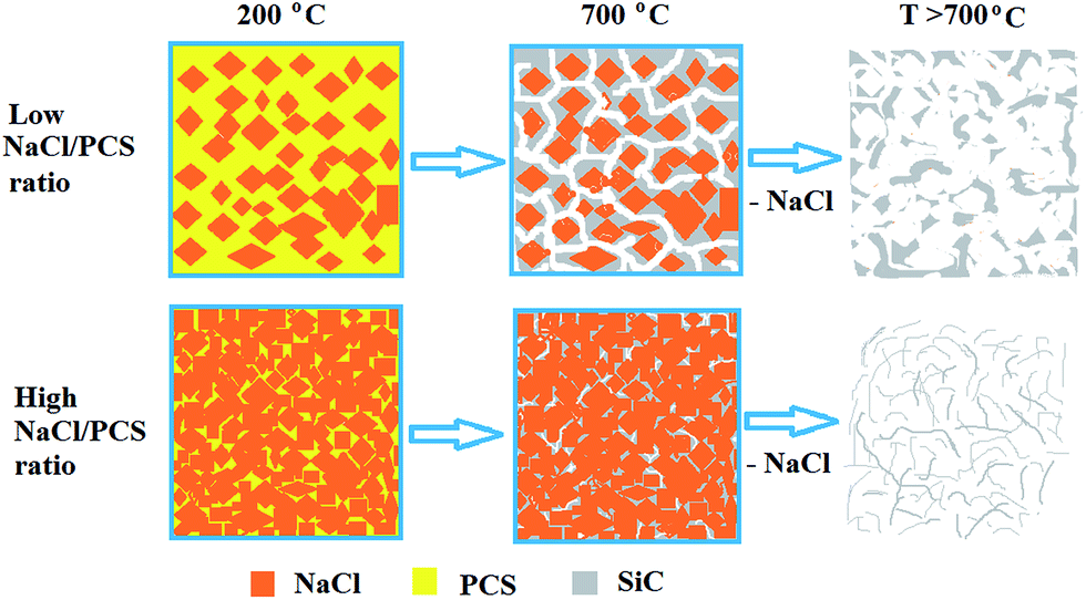 | ||
| Fig. 1 Schematic representation of the process for the synthesis of 3C–SiC nanoflakes in a NaCl powder template. | ||
Experimental
Materials
PCS was purchased from Nabond (MW = 1500–2500), while tetrahydrofuran (THF, anhydrous, 99.7%) and NaCl (99+%) were purchased from Alfa Aesar. Ar (99.999%) was used as the inert atmosphere. All the chemicals were used as received, without further purification.In the typical synthesis procedure, NaCl was first manually ground and then soaked in a 5 wt% solution of PCS in THF to obtain a thick paste. After the THF evaporated, the PCS/NaCl mixture was loaded into an alumina crucible and heated to 700 °C under an Ar flow for 5 h. In a parallel experiment, dry PCS was added to the NaCl powder and manually ground together for 30 minutes before being loaded in the furnace and heated under the same conditions. The resulted samples (consisting of pyrolyzed PCS and NaCl) were washed several times with deionised H2O to remove the salt. A dark brown powder was recovered through centrifugation and was subsequently air dried at 55 °C, for few hours. The collected powder (pyrolyzed PCS) was then heated to temperatures between 990–1200 °C for different periods of time to promote the crystallisation of SiC. The yield of SiC was approximately 50 wt% with respect to the initial mass of PCS. Upon examination by scanning electron microscopy, no difference in morphology was observed when a PCS/THF solution or only dry PCS was used. Also, no difference in the morphology of the samples that were ground after the addition of PCS/THF solution and of the samples that were not ground after the NaCl was soaked with PCS/THF solution was noticed.
Characterisation
X-ray diffraction (XRD) analysis was performed with a PANalytical X'pert Pro diffractometer with Cu Kα radiation and an X'celerator detector. The diffraction patterns were recorded in the 2-theta range from 20° to 90° with a step size of 0.5° and a collection time of 100 s per step. The diffraction patterns were analyzed for the phase composition using H'Pert HighScore software. For the estimation of the crystallite size using the Scherrer equation, the full width at half maximum (FWHM) of the most intense peak was used.The microstructure was investigated with a scanning electron microscope (SEM) model JEOL JSM 7100F, in a secondary electron mode. For this analysis, the samples were first dispersed in ethanol, then sonicated in an ultrasonic bath for 15 minutes. Afterwards, a drop of this dispersion was added onto a Si wafer. After the solvent evaporated, the Si wafer was fixed on the sample holder using a carbon tape. An accelerating voltage of 20 kV was used for all the samples.
Transmission electron microscopy (TEM) analysis was performed with a transmission electron microscope model JEOL JEM 2100 HR, operating at 200 kV. For the TEM analysis, a dilute dispersion of SiC flakes in ethanol was first prepared. The dispersion was transferred to an ultrasonic bath for 15 min and then deposited on a lacey carbon-coated TEM grid by immersing the grid for few seconds in this dispersion and then air dried.
Fourier transform infrared (FT-IR) spectra were recorded in attenuated total reflectance (ATR) mode on a FT-IR spectrophotometer (Perkin Elmer Spectrum 100 FT-IR) equipped with TGS detector and an ATR module. For each measurement, the powder was pressed on the ATR (diamond) window (d = 2 mm) and each spectrum was collected from 32 scans accumulation, each with a nominal resolution of 4 cm−1 in the region 400–4000 cm−1. The background was measured with the ATR module without any sample.
The room temperature Raman spectra were recorded on the powder, in a 180° backscattering geometry, after 10 recordings, with a Horiba Jobin-Yvon Lab RAM HR spectrometer equipped with a holographic notch filter and a CCD detector, by using the 632.8 nm excitation line of a 20 mW HeNe laser. The samples were placed on an Olympus BX 40 microscope equipped with a 50× objective and the laser beam was focused on the sample to give a spot size of 1 μm. The spectra were recorded in the range of 50–4000 cm−1.
The texture characteristics were determined by low-temperature (77.4 K) nitrogen adsorption in a Quantachrome Instruments NOVA 1200e (USA) apparatus. The nitrogen adsorption–desorption isotherms were analyzed to evaluate the following parameters: the specific surface areas (SBET) determined on the basis of the BET equation, the total pore volume (Vt) estimated in accordance with the Gurvich rule at a relative pressure close to 0.99, and the pore size distribution (PSD) calculated using the BJH method.
Results and discussions
The microstructure of the as-obtained samples was investigated by SEM. It was found that the morphology of the particles changed drastically with the NaCl/PCS weight ratio. Big particles with dimensions ranging from 80–100 μm formed when the NaCl/PCS ratio was 1:1 (Fig. 2A). These particles were microcracked but with some smooth surfaces formed at the faces of the NaCl crystallites.
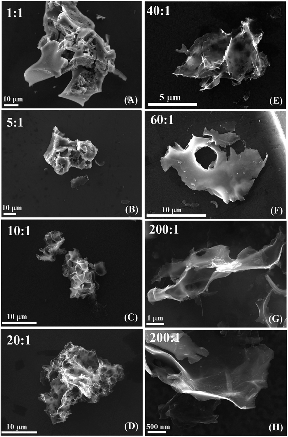 | ||
| Fig. 2 SEM images of the SiC samples obtained by pyrolysis of PCS at different NaCl/PCS ratios. | ||
As the NaCl/PCS ratio increased to 5:1, the particles size decreased to about 60 μm (Fig. 2B). The morphology changed so that the particles show cavities with non-uniform shapes and volumes reflecting the morphology of the NaCl template. With the increase in the NaCl/PCS ratio to 10:1 (Fig. 2C), the mean particle size decreased to about 20 μm. In this case, the particles have a foamy-like structure. The morphology remained the same for the ratio of 20:1 (Fig. 2D). It appears that the cell walls become thinner as bigger cavities are formed. At a further increase in the NaCl/PCS ratio to 40:1 the particles split to form a “W” shape (Fig. 2E).
For the NaCl/PCS ratio of 60:1, the particle size remained in the range of 5 to 10 μm. At this ratio, the particles look like thin flakes with some holes of few micrometers in diameter (Fig. 2F). No noticeable change in the morphology of the particles can be seen for the NaCl/PCS ratio of 200:1 (Fig. 2G and H). It is difficult to estimate the thickness of these flakes since they are non-uniform, but from the SEM analysis it can be approximated that they are about 5 nm at the edges and up to 50–60 nm in the thicker regions.
Aforementioned findings indicate the existence of a critical NaCl/PCS ratio of about 40:1, at which the sheet-like structure of the SiC particles prevails. We assume that the reason behind this is a critical film thickness of the melted PCS film. Below this thickness, the liquid film ruptures.
To estimate this value, a theoretical critical film thickness of the liquid PCS on the NaCl surfaces, hc, was calculated using an equation developed by Manev and Nguyen37 (eqn (1)):
| hc = (Aλc2/128σ)1/4 | (1) |
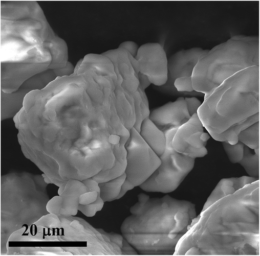 | ||
| Fig. 3 A SEM image of the NaCl particles used in the synthesis of the SiC nanometer thin flakes. | ||
Fig. 4 shows the XRPD patterns of the samples obtained when the pyrolysed PCS (NaCl/PCS ratio of 40:1) was heated at different temperatures, in Ar flow. It can be seen that the XRD pattern of the SiC flakes obtained at a temperature of 990 °C shows only a broad peak at 2-theta of 31.7° and this indicates that the flakes obtained at this temperature are amorphous.
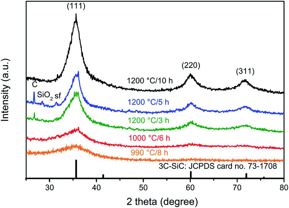 | ||
| Fig. 4 XRPD patterns of the solids resulted when the pyrolysed PCS (from a NaCl/PCS ratio of 40:1) was heated at different temperatures, in Ar flow. | ||
At 1000 °C, a long-range order starts to develop as it is suggested by the onset of sharpening of this peak. As expected, a further increase in temperature to 1200 °C leads to a notable difference in the XRD patterns. At this temperature, three peaks that correspond to the characteristic planes of 3C–SiC, (111), (220), and (311) are clearly visible. As indicated by the broadness of the SiC diffraction peaks, the thermal treatment at 1200 °C for 3 h results in a SiC with a poor crystallinity and very small crystallite size.
With the increase in the dwell time to 5 h and 10 h, a further increase in the crystallinity and growth of the crystal size occurs as it is suggested by the more intense and sharper diffraction peaks. The mean crystallite size for the sample obtained at 1200 °C/10 h was calculated with Scherrer equation38 (it was assumed that the peak broadening was caused only by the grain size, the microstrain and inhomogeneity of the sample were neglected) and it was found to be 3.65 nm.
Two additional small peaks corresponding to carbon and SiO2 phases are also noticeable but only for the samples obtained at 1200 °C after 3 and 5 h, respectively. It is well-known that the conversion of PCS to SiC will always result in the formation of residual carbon and some SiO2 – usually as a protective silica layer on the SiC material.39 While the presence of C is due to a nonstoichiometric C/Si ratio in the PCS, SiO2 can result from absorption of oxygen or moisture in raw PCS or oxygen entering the system during pyrolysis.
Judging only from the XRD analysis, one can see that the sample obtained at 1200 °C/10 h is composed of only 3C–SiC. No impurities are detected for this sample, only one additional small peak located at 2-theta of 31.7°, which corresponds to the staking faults, sf. Sf are the most common defects in 3C–SiC and they are regions of incorrect stacking of the crystal planes or twin boundaries.40,41 However, evidence for the presence of some turbostratic C in this sample was later found from TEM and Raman analyses.
To further investigate the microstructure and phase composition of the SiC flakes, TEM, Raman, and IR analyses were performed. TEM images on the SiC samples obtained at different temperatures are shown in Fig. 5–8.
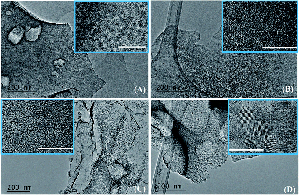 | ||
| Fig. 5 TEM images of the SiC flakes obtained from a NaCl/PCS ratio of 40:1, heated at different temperatures and for different periods of time: 1000 °C/6 h (A), 1200 °C/3 h (B), 1200 °C/5 h (C), and 1200 °C/10 h (D). The insets are a high magnification image on the corresponding flake. The scale bar in all the insets is 10 nm. | ||
 | ||
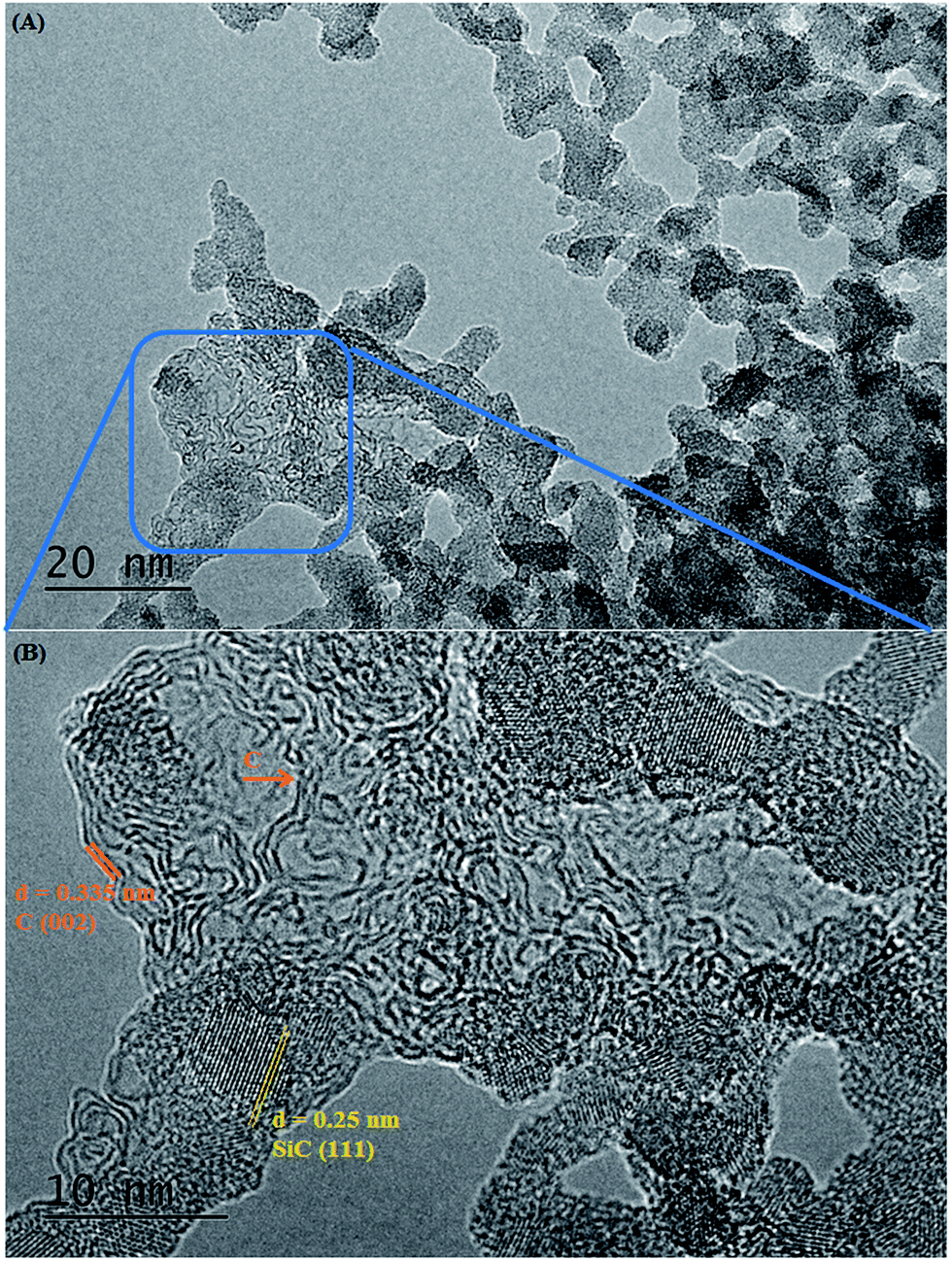
| Fig. 6 TEM images of a SiC flake obtained at 1200 °C/5 h, from a NaCl/PCS ratio of 40:1. | ||
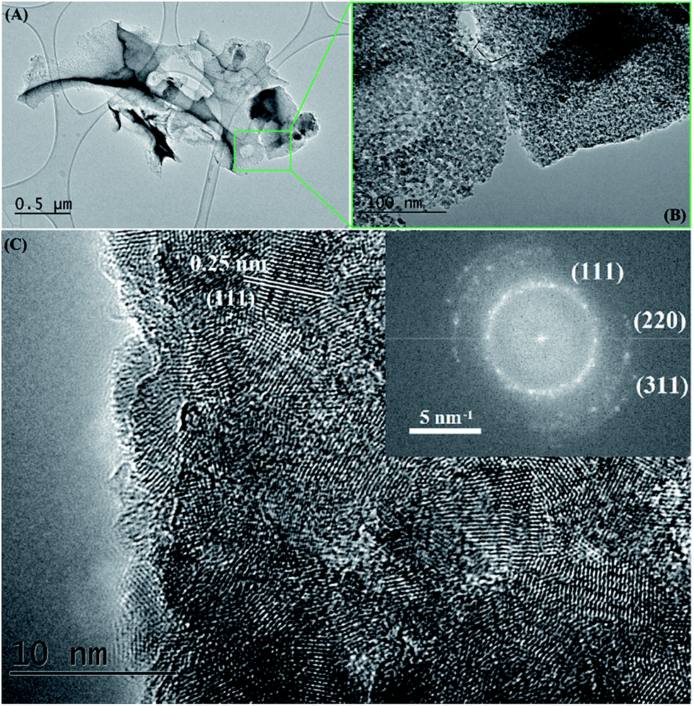 | ||
| Fig. 7 TEM images of a SiC flake obtained at 1200 °C/10 h, from a NaCl/PCS ratio of 40:1. The inset is the corresponding fast Fourier transform pattern. | ||
 | ||
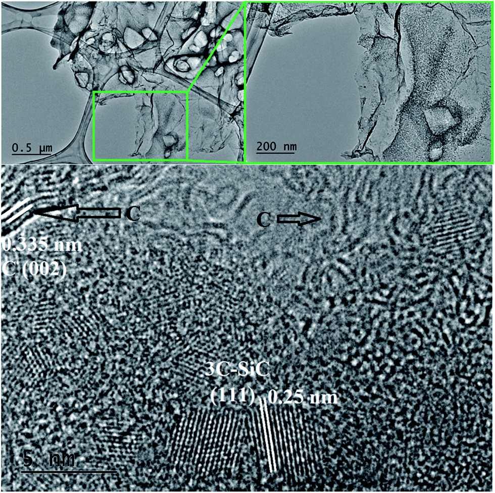
| Fig. 8 (A) Additional TEM image of a SiC flake obtained at 1200 °C/10 h from a NaCl/PCS ratio of 40:1; (B) this HRTEM image shows that an additional phase with the interplanar distance of 0.335 nm (carbon) is sometimes observed among the SiC nanocrystals. | ||
Fig. 5A–D shows a selection of TEM and HRTEM (as insets) images of samples obtained at different temperatures and dwell times. At a temperature of 1000 °C/6 h (Fig. 5A) the samples look like thin sheets with some rectangular holes (produced after the deionised water washed away the NaCl particles) and there is no obvious long-range order (see the inset in Fig. 5A).
A higher temperature of 1200 °C with a dwell time of 3 h does not result in a significant change of the texture or crystallinity. In the inset in Fig. 5B there is though a suggestion of some embryonic ordering from the presence of few SiC crystalline areas in an amorphous matrix. A further small increase in the dwell time from 3 to 5 h leads to a drastic change in both texture and crystallinity. Fig. 5C clearly shows the presence of small crystallites in a thin sheet-like matrix. A closer look at the inset in Fig. 5C reveals that those spots are circular crystalline structures of about 2 nm in diameter with clearly visible lattice fringes. After 10 h at 1200 °C, these crystallites grew to a size of about 4 nm and became interconnected as a result of the complete crystallisation and crystal growth (Fig. 5D). TEM analysis is in agreement with the XRD data which showed that the crystallinity of the samples increases progressively with increasing the dwell time from 3 to 10 h at 1200 °C. Additional TEM images on the SiC flakes thermally treated at 1200 °C/5 h are shown in Fig. 6. These images of SiC flakes freely suspended on a lacey carbon coated TEM grid further confirm their sheet-like morphology. The SiC samples also have few voids which were probably produced after the deionised water washed away the NaCl particles. Nanocrystallites of 3C–SiC (d = 0.25 nm) with an average size of 2.7 nm (determined with the ImageJ software) and different forms of carbon (turbostratic and onion-like carbon, with d = 0.335 nm) can also be observed in these images.
Bright field TEM images of the sample obtained at the same temperature of 1200 °C but with a 10 h dwell time are shown in Fig. 7. At a closer look (Fig. 7B), it can be seen that the flake is polycrystalline and it is composed only of SiC crystallites with average size 3.7 nm (most of them being between 2–5 nm), value which is in excellent agreement with the crystallite mean size calculated by XRD (3.65 nm). Crystallites are randomly oriented and different orientations are observed in the TEM image, distinguishable from different interplanar distances (0.25 nm for the (111) plane but also along the (220) and (311) planes) as shown in the corresponding Fast Fourier Transform (FFT) pattern (in the inset of the Fig. 7C). Additional TEM analyses on a different part of this flake (Fig. 8) show that some of the flakes are composed not only of 3C–SiC nanocrystallites (d = 0.25 nm), but also graphene-like or onion-like carbon (with d = 0.335 nm).
Raman analysis (Fig. 9) also suggests that some free carbon is present in this sample. In Fig. 9, the two Raman spectra (for the sample obtained at 1000 °C/6 h and after crystallisation – 1200 °C/10 h) look very similar. The amorphous sample (1000 °C/6 h) shows two main peaks at 1322 and 1603 cm−1, plus some small peaks at around 458, 611, 864, 959, 1160, 2623 and 2911 cm−1. The band located at 1160 cm−1 corresponds to the ν1 mode of transpolyacetylene;42,43 at 1322 cm−1 is the D band of carbon (so called “disorder” band) which corresponds to the zone center phonons of E2g symmetry and it is associated with the structural imperfections or symmetry loss. The peak at 1603 cm−1 is the G (or graphitic) mode which is assigned to the A1g mode (in plane vibrational mode) of carbon. The peak at 2623 cm−1 is a second order overtone of the D mode (also named “2D”) whereas the peak at 2911 cm−1 is the D′ or D + G peak (a combination scattering peak). An increase in the temperature to 1200 °C resulted in disappearance of the peak at 1160 cm−1, a redshift of the G peak from 1603 to 1589 cm−1, and a narrowing of both D and G peaks. The redshift and narrowing of the G peak might indicate an increase in the ordering of the carbon phase.44 The ID/IG ratio (I is the intensity of the peak) is related to the degree of carbon amorphisation.45 In our case, the ID/IG ratio is having a value of 1.43 and 1.37, for the amorphous and crystalline SiC, respectively and this further suggests that in both samples, the carbon could exist in the form of few graphene layers.
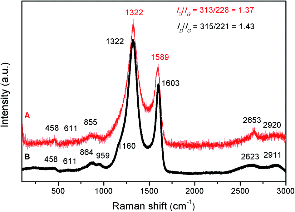 | ||
| Fig. 9 Raman spectra of SiC samples obtained at two different temperatures, before (1000 °C/6 h – spectrum B) and after crystallisation (1200 °C/10 h – spectrum A). | ||
The small peaks located at 458 and 611 cm−1 correspond to the Si–O–Si bonds, whereas the ones located at about 860 and 959 cm−1 are probably the TO and LO Raman modes of SiC. Due to a better Raman scattering efficiency of the C–C bonds compared to the Si–C ones, and for such small SiC crystallites, the Raman lines characteristic of crystalline SiC become almost unobservable.46 The residual carbon observed along with the SiC phase can be beneficial in photocatalytic processes where it can serve as electron-accepting sites, facilitating the interface charge separation. But if desired, this residual carbon can also be removed by heating in air at approximately 600 °C.
ATR analysis of the samples obtained at 1000 °C/6 h and 1200 °C/10 h (Fig. 10) shows that both samples consist of mainly SiC. At 1000 °C, a broad absorption band at 771 cm−1 and two small shoulders at 467 and 1090 cm−1 are observed. The strongest band (771 cm−1) corresponds to the Si–C bond stretching mode, while the weak absorption bands (467 and 1090 cm−1) could be assigned to Si–O symmetric and asymmetric stretching modes. With an increase in temperature to 1200 °C and, therefore, an increase in the crystallinity, these bands become narrower. As also indicated by ATR analysis, the SiC obtained at 1200 °C/10 h contains a very small amount of silicon dioxide. This SiO2 can be removed by washing with a small amount of diluted hydrofluoric acid.47
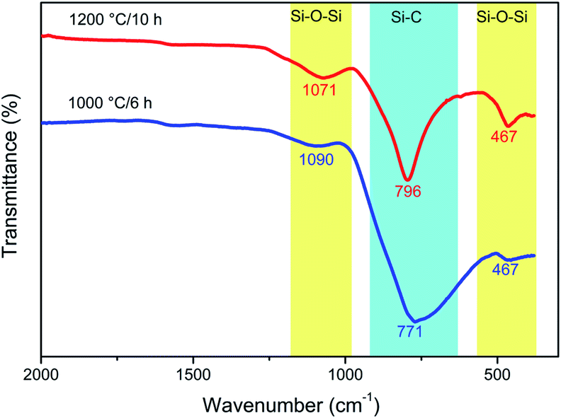 | ||
| Fig. 10 ATR spectra of two SiC samples obtained at two different temperatures, before (1000 °C/6 h) and after (1200 °C/10 h) crystallisation. | ||
To obtain quantitative morphologic information about the samples, nitrogen adsorption was measured at 77.4 K. The specific surface area was calculated using the BET method (SBET). The isotherms were analysed to determine the total pore volume (Vt) and the pore size distribution (PSD).
To investigate the effect of the NaCl/PCS ratio on the SBET, fourteen samples were selected, as shown in Table 1.
| NaCl to PCS weight ratio | Obtained at 700 °C | Obtained at 1200 °C | ||||
|---|---|---|---|---|---|---|
| SBET (m2 g−1) | Vt, (cm3 g−1) | D (nm) | SBET (m2 g−1) | Vt, (cm3 g−1) | D (nm) | |
| 1:1 |
8 | 0.02 | 7 | 4 | 0.05 | 4.5 |
| 5:1 |
13 | 0.02 | 5 | 9 | 0.01 | 5.8 |
| 10:1 |
8 | 0.02 | 9.5 | 24 | 0.03 | 4.6 |
| 20:1 |
10 | 0.02 | 10 | 64 | 0.10 | 6 |
| 40:1 |
15 | 0.07 | 19 | 169 | 0.19 | 4.5 |
| 60:1 |
21 | 0.09 | 16 | 68 | 0.12 | 7.2 |
| 200:1 |
163 | 0.75 | 1.81 | 72 | 0.26 | 14 |
As already revealed by SEM, the BET analyses indicate that a fine tuning of the NaCl/PCS ratio clearly results in the evolution of diverse morphologies. For the samples obtained at the temperatures lower than the crystallisation temperature, the SBET increased with the NaCl/PCS ratio from a value of 8 m2 g−1 (1:1 ratio) up to a maximum value of 163 m2 g−1 (200:1 ratio). This high SBET is associated with a very high value of the Vt of 0.75 cm3 g−1. Also the SBET of the crystalline samples increased with the NaCl/PCS ratio, from 4 m2 g−1 (1:1) up to a value of 72 m2 g−1 (200:1). When NaCl/PCS ratio was below 10:1, the SBET of the SiC obtained at 1200 °C was lower than that at 700 °C. At 1200 °C, as the crystallisation occurs, Si–C bonds rearrange to form a more dense structure which could lead to a decrease of the SBET. The samples obtained from a NaCl/PCS ratio ≥ 20:1 showed a bigger SBET at 1200 °C than at 700 °C, except for the sample obtained from a NaCl/PCS ratio of 200:1, which shows decreased SBET. It is interesting to observe that at 1200 °C, the largest SBET belongs to the sample obtained from a NaCl/PCS ratio of 40:1.
Conclusions
In this work, a facile synthetic route to 3C–SiC nanoflakes by pyrolysis of PCS in a NaCl template at 700 °C, followed by crystallisation at 1200 °C, was developed. It was found that the weight ratio between NaCl and PCS is dictating the morphology of the SiC particles. A critical NaCl/PCS ratio for the formation of the nanoflakes has been determined to be around 40:1. These nanometer thin SiC flakes exhibit a high specific surface area of up to 169 m2 g−1 and a high total pore volume of up to 0.75 cm3 g−1 – properties which can be finely tuned by the adjustment of the NaCl/PCS ratio.
This method is a simple, versatile and robust way for the production of SiC nanostructures. Such a facile synthetic method could bring nanostructured SiC one step closer to the ultimate goal of practical applications such as in Li-ion batteries, for hydrogen evolution and/or storage, as anticorrosive surfaces, solar cells, fuel cells and other applications.
Acknowledgements
We are grateful to the Ministry of Education, Science and Sport of the Republic of Slovenia for the financial support through the postdoctoral/early career grant (JR RK-13) “Raziskovalci na začetku kariere”. We also acknowledge the financial support of the Slovenian Research Agency Program P2-0377.Notes and references
- D. H. Van Dorp, N. Hijnen, M. Di Vece and J. J. Kelly, Angew. Chem., Int. Ed., 2009, 48, 6085 CrossRef CAS PubMed.
- J. Fan and P. K. Chu, Small, 2010, 19, 2080 CrossRef PubMed.
- E. S. Saddow, Silicon Carbide Biotechnology: A Biocompatible Semiconductor for Advanced Biomedical Devices and Applications, Elsevier, Amsterdam, 2012 Search PubMed.
- W. H. Backes, P. A. Bobbert and W. van Haeringen, Phys. Rev. B: Condens. Matter Mater. Phys., 1994, 49, 7564 CrossRef CAS.
- J. Fan and P. K. Chu, Silicon Carbide Nanostructures: Fabrication, Structure, and Properties, Springer International Publishing, Switzerland, 2014 Search PubMed.
- J. Y. Fan, X. L. Wu and P. K. Chu, Prog. Mater. Sci., 2006, 51, 983 CrossRef CAS.
- J. Fan, H. Li, J. Jiang, L. K. Y. So, Y. W. Lam and P. K. Chu, Small, 2008, 4, 1058 CrossRef CAS PubMed.
- Y. Zakharko, T. Nychyporuk, L. Bonacina, M. Lemiti and V. Lysenko, Nanotechnology, 2013, 24, 055703 CrossRef CAS PubMed.
- X. Lin, S. Lin, Y. Xu, A. Hakro, T. Hasan, B. Zhang, B. Yu, J. Luo, E. Li and H. Chen, J. Mater. Chem. C, 2013, 1, 2131 RSC.
- W. Zhou, L. Yan, Y. Wang and Y. Zhang, Appl. Phys. Lett., 2006, 89, 013105 CrossRef.
- J.-Y. Hao, Y.-Y. Wang, X. L. Tong, G. Q. Jin and X.-Y. Guo, Int. J. Hydrogen Energy, 2012, 37, 15038 CrossRef CAS.
- Z. Cheng, F. Bing, Q. Liu, Z. Zhang and X. Fang, J. Mater. Chem. A, 2015, 3, 4652 Search PubMed.
- S. D. T. Kumari, D. Jeyakumar and T. P. Kumar, RSC Adv., 2013, 3, 15028 RSC.
- C. He, X. Wu, J. Shen and P. K. Chu, Nano Lett., 2012, 12, 1545 CrossRef CAS PubMed.
- G. Mpourmpakkis and G. E. Froudakis, Nano Lett., 2006, 8, 1581 CrossRef PubMed.
- M. Wang, J. Chen, X. Liao, Z. Liu, J. Zhang, L. Gao and Y. Li, Int. J. Hydrogen Energy, 2014, 39, 14581 CrossRef CAS.
- G. Mishra, K. M. Parida and S. K. Singh, ACS Sustainable Chem. Eng., 2015, 3, 245 CrossRef CAS.
- K. V. Emtsev, A. Bostwick, K. Horn, J. Jobst, G. L. Kellogg, L. Ley, J. L. McChesney, T. Ohta, S. A. Reshanov, J. Röhrl, E. Rotenberg, A. K. Schmid, D. Waldmann, H. B. Weber and T. Seyller, Nat. Mater., 2009, 8, 203 CrossRef CAS PubMed.
- P. Mavinakuli, S. Wei, Q. Wang, A. B. Karki, S. Dhage, Z. Wang, D. P. Young and Z. Guo, J. Phys. Chem. C, 2010, 114, 3874 CAS.
- Z. Guo, T. Y. Kim, K. Lei, T. Pereira, J. G. Sugar and H. T. Hahn, Compos. Sci. Technol., 2008, 68, 164 CrossRef CAS.
- J. Chen, J. Zhang, M. Wang and Y. Li, Sens. Actuators, B, 2014, 201, 402 CrossRef CAS.
- J. Chen, X. Liao, M. Wang, Z. Liu, J. Zhang, L. Ding, L. Gao and Y. Li, Nanoscale, 2015, 7, 6374 RSC.
- S. Yang, W. Cai, H. Zeng and X. Xu, J. Mater. Chem., 2009, 19, 7119 RSC.
- T. Seeger, P. Kohler-Redlich and M. Rühle, Adv. Mater., 2000, 12, 279 CrossRef CAS.
- Y. Y. Choi and D. J. Choi, CrystEngComm, 2013, 15, 6963 RSC.
- G. W. Meng, Z. Cui, L. D. Zhang and F. Philipp, J. Cryst. Growth, 2000, 209, 801 CrossRef CAS.
- S. Chabi, H. Chang, Y. Xia and Y. Zhu, Nanotechnology, 2016, 27, 075602 CrossRef PubMed.
- J. Chen, Q. Shi, L. Gao and H. Zhu, Phys. Status Solidi A, 2010, 207, 2483 CrossRef CAS.
- J. Chen, J. Zhang, M. Wang, L. Gao and Y. Li, J. Alloys Compd., 2014, 65, 168 CrossRef.
- L. Xin, Q. Shi, J. Chen, W. Tang, N. Wang, Y. Liu and Y. Lin, Mater. Charact., 2012, 65, 55 CrossRef CAS.
- R. D'Amato, M. Falconieri, S. Gagliardi, E. Popovici, E. Serra, G. Terranova and E. Borsella, J. Anal. Appl. Pyrolysis, 2013, 114, 461 CrossRef.
- X. Liu, M. Antonietti and C. Giordano, Chem. Mater., 2013, 25, 2021 CrossRef CAS.
- J. Zhu, Z. Liu, X. L. Wu, L. L. Xu, W. C. Zhang and P. K. Chu, Nanotechnology, 2007, 18, 365603 CrossRef.
- I. K. Sung, S. B. Yoon, J.-S. Yu and D.-P. Kim, Chem. Commun., 2002, 14, 1480 RSC.
- K.-H. Park, I.-K. Sung and D.-P. Kim, J. Mater. Chem., 2004, 14, 3436 RSC.
- N. Baccile, F. Babonneau, B. Thomas and T. Coradin, J. Mater. Chem., 2009, 19, 8537 RSC.
- E. D. Manev and A. V. Nguyen, Adv. Colloid Interface Sci., 2005, 114–115, 133 CrossRef CAS PubMed.
- P. Scherrer, Nachr. Ges. Wiss. Goettingen, Math.-Phys. Kl., 1918, 1918, 98 Search PubMed.
- E. Bouillon, F. Langlais, E. Pailler, E. Naslain, F. Cruege, J. C. Houng Sarthou, A. Delpuech, C. Laffon, P. Lagarde, M. Monthioux and A. Oberlin, J. Mater. Sci., 1991, 26, 1333 CrossRef CAS.
- E. J. Olivier and J. H. Neethling, Int. J. Refract. Met. Hard Mater., 2009, 27, 443 CrossRef CAS.
- U. Lindefelt, H. Iwata, S. Öberg and P. Briddon, Phys. Rev. B: Condens. Matter Mater. Phys., 2003, 67, 155204 CrossRef.
- A. C. Ferrari and J. Robertson, Philos. Trans. R. Soc., A, 2004, 362, 2477 CrossRef CAS PubMed.
- C. Castiglioni, M. Tommasini and G. Zerbi, Philos. Trans. R. Soc., A, 2004, 362, 2425 CrossRef CAS PubMed.
- S. Karlin and P. Colomban, J. Raman Spectrosc., 1997, 28, 219 CrossRef CAS.
- A. C. Ferrari and J. Robertson, Phys. Rev. B: Condens. Matter Mater. Phys., 2001, 64, 075414 CrossRef.
- E. Bouillon, F. Langlais, R. Pailler, R. Naslain, F. Cruege and P. V. Huong, J. Mater. Sci., 1991, 26, 1333 CrossRef CAS.
- G. Wei, W. Qin, K. Zheng, D. Zhang, J. Sun, J. Lin, R. Kim, G. Wang, P. Zu and L. Wang, Cryst. Growth Des., 2009, 9, 1431 CAS.
| This journal is © The Royal Society of Chemistry 2016 |