
Porous silicon nano-aggregate from silica fume as an anode for high-energy lithium-ion batteries†
Tianwen
Zhang
a,
Lei
Hu
a,
Jianwen
Liang
a,
Ying
Han
a,
Yue
Lu
a,
Yongchun
Zhu
*a and
Yitai
Qian
*ab
aHefei National Laboratory for Physical Science at Microscale and Department of Chemistry, University of Science and Technology of China, Hefei, Anhui 230026, P. R China
bSchool of Chemistry and Chemical Engineering, Shandong University, Jinan 250100, P. R. China
First published on 16th March 2016
Abstract
A porous silicon nano-aggregate (PSNA) has been prepared using a ‘‘conproportionation’’ reaction of magnesium silicide and silica fume, which is a waste by-product from the manufacture of metallurgical grade silicon. The as-prepared PSNA, with a pore diameter of 10–100 nm, is composed of Si nanoparticles with diameters of 10–50 nm. As an anode for a rechargeable lithium ion battery, it delivers a high reversible specific capacity (3224 mA h g−1 at 0.36 A g−1) and significant cycling stability (~90% capacity retention after 500 cycles and ~69% capacity retention even after 1000 cycles at a current density of 1.8 A g−1).
Si has been considered as a key potential anode material due to its high theoretical capacity of 4200 mA h g−1 and low working potential (~0.5 V versus Li/Li+).1–5 However, Si exhibits serious volume changes (~400%) during the lithiation and delithiation process, which leads to pulverization of the electrode and a rapid reduction in capacity.1,5–8
To overcome this problem, many efforts have been made in the design of porous or nanostructured Si-based materials. For example, porous Si/C composites were prepared using a facile sacrificing method and showed a reversible capacity of 800 mA h g−1 after 220 cycles.9 Nanoporous silicon networks were fabricated using an electrochemical process, delivering a reversible capacity of 1000 mA h g−1 at 1C after 200 cycles.10 Nanoporous silicon was obtained from rice husks using a magnesiothermic reaction, exhibiting a reversible capacity of 2790 mA h g−1 at 2.1 A g−1and ~86% capacity retention after 300 cycles.11
In addition, converting Mg2Si powders into nano-Si or porous Si is an alternative route to obtain nano-silicon. For example, silicon nanoclusters have been prepared through the reaction of Mg2Si and SiCl4 in organic solvents.12 Recently, a nano-silicon/carbon mesoporous composite was produced through the reaction of Mg2Si and amorphous silica using a high energy mechanical milling process, delivering a reversible capacity of 1600 mA h g−1 over 50 cycles at a current density of 1.0 A g−1 and good rate capabilities with a reversible capacity of about 1530 mA h g−1 at a discharge current density of 3 A g−1.13
Silica fume is a waste by-product of the production of elemental silicon or ferrosilicon alloys in electric arc furnaces. Silicon smelters have been collecting silica fume and searching for its applications. Currently, silica fume has been mainly applied to admixtures for concrete and cementititous products. Discovering and recovering high-value materials from silica fume is desirable.
In this work, we synthesize a porous silicon nano-aggregate (PSNA), which is composed of many Si nanoparticles, using silica fume and Mg2Si as silicon sources. An intuitive process for synthesizing PSNAs is shown in Scheme 1.
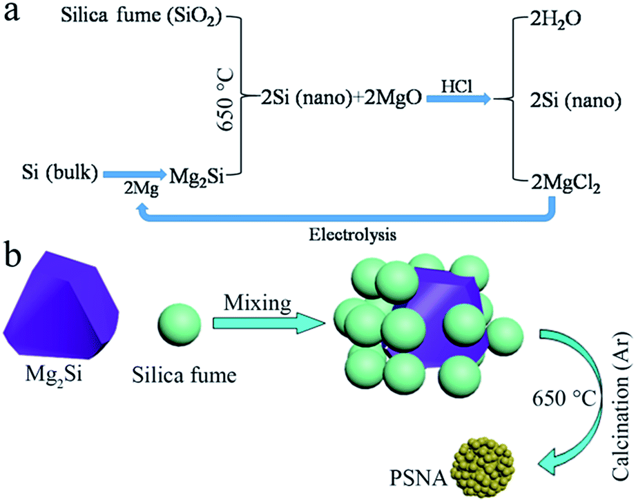 | ||
| Scheme 1 (a) Flow chart of the process for synthesizing PSNAs. (b) Schematic illustration of the formation of a PSNA. | ||
The reactions can be described as follows:
| 2Mg + Si(bulk) = Mg2Si | (1) |
| Mg2Si + SiO2 = 2Si(nano) + 2MgO | (2) |
| 2Si(nano) + 2MgO + 4HCl = 2Si(nano) + 2MgCl2 + 2H2O | (3) |
This method can provide nano-silicon twice based on the amount of Mg2Si,14,15 and is an alternative way to treat silica fume. When evaluated as an anode material for lithium-ion batteries, the as-synthesized PSNA electrode can deliver a high charge capacity of 1988 mA h g−1 after 500 cycles (1539 mA h g−1 even after 1000 cycles) at a relatively high current density of 1.8 A g−1.
The raw product obtained in eqn (2) without any treatment is examined using X-ray diffraction (XRD) analysis, the results of which are presented in Fig. 1a. The reflection peaks can be assigned to the mixture of Si (labeled ‘‘■’’, JCPDS no. 27-1402) and MgO (labeled “●”, JCPDS no. 45-0946). The XRD pattern of the sample after washing with dilute HCl solution is displayed in Fig. 1b. All of the peaks in Fig. 1b can be indexed as cubic Si with a calculated lattice constant a = 5.433 Å, which is very close to the reported value (JCPDS no. 27-1402). Based on the Sherrer equation, the size of the Si nanoparticles is estimated to be about 30 nm. Fig. S1† shows the SEM images of silica fume (Fig. S1a†) and Mg2Si (Fig. S1b†). As can be seen, silica fume is made up of spherical particles with an average particle diameter of 150 nm and the as-prepared Mg2Si is an irregular block material with a diameter of about 10–30 µm. The related XRD pattern of Mg2Si is shown in Fig. S2,† which confirms that bulk Si was converted to Mg2Si and without Mg existing. Fig. 1c is the SEM image of the sample after the reaction of Mg2Si and silica fume followed by HCl treatment. It clearly shows that the sample is composed of irregular nano-aggregates. From the corresponding transmission electron microscopy (TEM) image (Fig. 1d), it can be distinctly observed that the PSNA is composed of many Si nanoparticles with diameters of 10–50 nm. Fig. 1e shows the high-resolution TEM (HRTEM) image of the PSNA, revealing a 2–3 nm amorphous layer covering the Si nanoparticles. The interplanar distances are measured to be about 0.33 nm, corresponding to the (111) crystallographic planes of the Si nanocrystals. From the inset of Fig. 1e, many defects and dislocations can be observed, which indicate the presence of many grain boundaries in the sample. Besides, from the typical SAED pattern of the PSNA (Fig. 1f), it can be identified that these crystals of silicon have a diamond cubic structure.
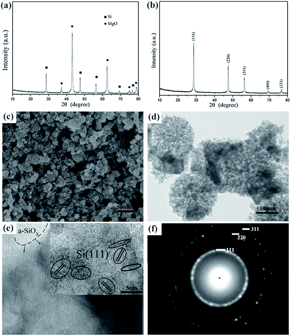 | ||
| Fig. 1 XRD pattern of (a) the sample without any treatment and (b) the same sample after HCl treatment. (c) SEM, (d) TEM, (e) HRTEM, and (f) SAED images of the sample. | ||
The Raman spectrum of the PSNA is shown in Fig. 2a. The sharp peak at 500 cm−1 is attributed to the Si–Si stretching mode of crystalline Si, which shifts to a lower frequency with a broadened full width at half maximum due to the diameter decrease.16 In addition, the two broad peaks at 292 and 930 cm−1 observed in Fig. 2a are assigned to the overtones of TA (X) and TO (L), respectively.17 They are related to the Si–Si stretching mode of the amorphous form.
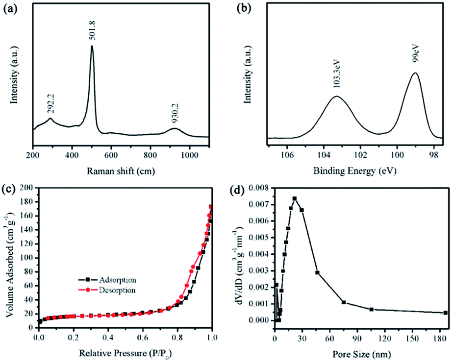 | ||
| Fig. 2 (a) Raman spectrum, (b) XPS spectrum and (c) N2 adsorption–desorption isotherms of the sample. (d) The pore-size distribution calculated from the desorption branch. | ||
The surface content of the PSNA is investigated using the Si 2p X-ray photoelectron spectroscopy (XPS) spectrum, as shown in Fig. 2b. A peak at ∼103 eV indicates the existence of SiOx.18 The results of the XPS and HRTEM indicate that a small amount of amorphous SiOx is on the surface of the Si nanoparticles. The conductivity of the PSNA samples, calculated using voltammetry (see calculation in Fig. S3†), is about 3.92 × 10⁻³ S m−1, which is generally close to that of the Si samples reported previously.19
The porous structure of the PSNA is characterized using N2 gas sorption measurements. The Brunauer–Emmett–Teller (BET, and Fig. 2c) specific surface area of the PSNA is calculated to be 57 m2 g−1. As a result, the PSNA can provide more sites for lithium storage, which maybe improves the electrochemical performance.20,21 Moreover, it can be observed from the pore size-distribution curve (Fig. 2d) that the size of most pores is in the range of 10–100 nm. These pores can be observed in the TEM micrographs (Fig. 1d).
In order to investigate the electrochemical performance of the PSNA electrode, we assembled a half-cell in which the PSNA electrode was paired with lithium foil.
Fig. 3a displays the cyclic voltammetry (CV) curves for the first, third and fifth cycles of the PSNA electrode in the potential window of 0.005–1.5 V vs. Li+/Li. As can be seen, the CV behavior is generally consistent with that of the Si-based nanostructures reported previously.22–25 The characteristic peaks of amorphous Si are located at ~0.21 V (cathodic peak), ~0.32 V (anodic peak) and ~0.51 V (anodic peak).22 In addition, both amorphous and crystalline Si have a characteristic peak at ~0.005 V. In the first cathodic scan, a peak which is located at ~0.005 V is observed, which is due to only crystalline Si existing.24 In the first anodic scan, two anodic peaks of amorphous Si (at ~0.32 and ~0.51 V) are observed, because the crystalline structure becomes amorphous during lithiation. The cathodic peak at 0.21 V corresponds to the conversion of crystalline Si to the LixSi phase,26 while the peak at ~0.51 V in the anodic process corresponds to the delithiation of amorphous (α)α-LixSi to α-Si.22 In the third and fifth cycles, the anodic peak at ~0.32 V was not present, partly because of the broadening and increase of the peak at ~0.51 V after the first cycle.27
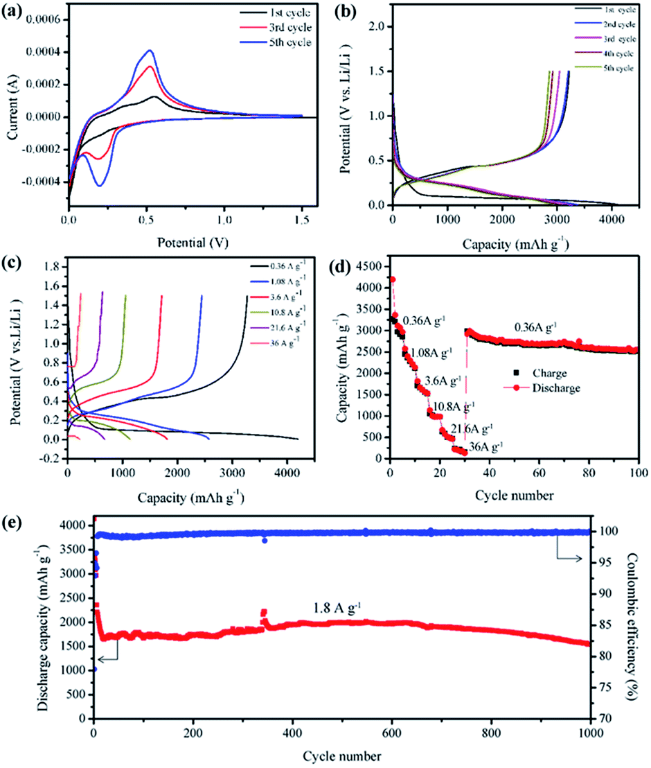 | ||
| Fig. 3 Electrochemical performances of the PSNA electrode. (a) Cyclic voltammetry curves of a typical PSNA electrode. (b) Typical galvanostatic discharge–charge curves for the first five cycles of the PSNA electrode in the potential region of 0.005–1.50 V versus Li/Li+ at 360 mA g−1. (c) The typical galvanostatic discharge–charge curves at different current densities. (d) The rate performance of the PSNA electrode. (e) Long term cycling property of the PSNA electrode at a current density of 0.36 mA g−1 for the first 5 cycles, and at 1.8 A g−1 for the rest of the cycles. | ||
Fig. 3b shows the typical voltage profiles for the first five cycles of the PSNA electrode at a current density of 360 mA g−1. The main discharge potential plateau is located near 0.1 V (vs. Li/Li+), which is assigned to the lithiation of crystalline Si and the formation of LixSi. The first discharge and charge capacities are 4136 and 3224 mA h g−1, respectively. The coulombic efficiency for the electrodes is 78% in the 1st cycle. The irreversible capacity of the first cycle is normally caused by the inevitable formation of a solid electrolyte interface (SEI) membrane which can result in an initial irreversible capacity loss and disappears in the following cycles.20
The rate capability of the PSNA electrode was evaluated using galvanostatic charge–discharge measurements at varying current densities from 0.36 A g−1 to 36 A g−1 (0.252 mA cm−2 to 25.2 mA cm−2 ) and then back to 0.36 A g−1 (as shown in Fig. 3c and d). It is obvious that the PSNA electrode delivers a capacity decrease from 3272 mA h g−1 at 0.36 A g−1 to 240 mA h g−1 at 36 A g−1. When the current density goes back to 0.36 A g−1, the capacity is able to return to a high value of 2986 mA h g−1. Even after the 100th cycle, the capacity retention is still as high as 2520 mA h g−1.
In addition, the long term cycling performance at a 1.8 A g−1 rate was also tested. As can be seen in Fig. 3e, the PSNA electrode exhibits a capacity retention of 1539 mA h g−1 at a current density of 1.8 A g−1 even after 1000 cycles. It should be mentioned that the first five cycles of the cells tested at a relatively low current density of 0.36 A g−1 are to activate the Si nanoparticles sufficiently. The corresponding coulombic efficiency curve of the PSNA is shown in Fig. 3e and the coulombic efficiency quickly increases from 78% for the first cycle to 95% for the second cycle and further reaches over 99% after several cycles, which is meaningful for practical applications. Remarkably, from the fifth to the 1000th cycle, more than 69% capacity retention is obtained.
We attribute the exceptional electrochemical stability to the well-developed porous structure and the amorphous SiOx layer coated on the surface of the PSNA electrode. Fig. 4 presents the surface morphology of the PSNA electrode before (Fig. 4a and b) and after (Fig. 4c and d) 1000 cycles. After 1000 deep cycles, the PSNA electrode is covered by a thin and uniform SEI layer and still maintains its integrity and shows no large cracks.
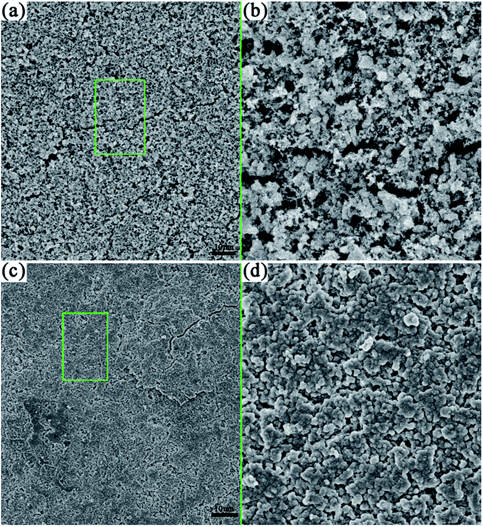 | ||
| Fig. 4 The surface morphology of the PSNA electrode before (a and b) and after (c and d) 1000 cycles. | ||
The enhanced lithium storage properties of the PSNA may be attributed to its unique structure which has multiple advantages as illustrated in Scheme 2. First, the existence of pores may effectively accommodate the volume change of silicon and allow for facile strain relaxation without strong mechanical stress during the Li+ ion insertion/de-insertion process. Second, the large BET surface area can increase the number of active sites and enhance the contact surface between the electrode material and electrolyte. Third, the amorphous SiOx layer coated on the surface of the PSNA can suppress the volume expansion and protect the PSNA from a side reaction with the electrolyte. Forth, our sample consists of many nanometric crystalline regions separated by interfacial regions. Owing to the disordered arrangement of the atoms at a grain boundary, the crystal structure is relatively loose, which would provide a fast diffusion path for electrons/lithium ions. Commonly, this disordered atom arrangement is associated with vacancies and dislocations which are generally favorable for improving the conductivity.
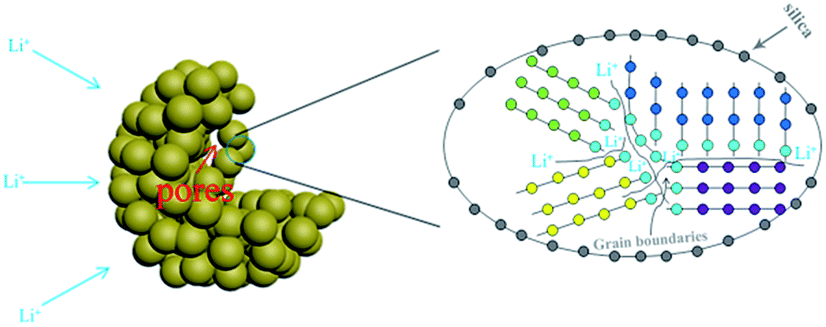 | ||
| Scheme 2 The illustration of the microstructure and transport paths of Li+ ions in the PSNA. | ||
Conclusions
In summary, we applied silica fume, a waste by-product, to synthesize a porous silicon nano-aggregate (PSNA) by reaction with Mg2Si. As an anode for a rechargeable lithium ion battery, the as-prepared PSNA exhibits high-performance with a high specific charge capacity (3224 mA h g−1 at 0.36 A g−1 and 2216 mA h g−1 at 1.8 A g−1) and long cycle life (~90% capacity retention after 500 cycles and ~69% capacity retention even after 1000 cycles at a current density of 1.8 A g−1).Acknowledgements
This work is supported by the Foundation for Innovative Research Groups of the National Natural Science Foundation of China (Grant 21521001); the National Natural Science Fund of China (No. 91022033 and 21201158); the Fundamental Research Funds for the Central Universities (No. WK2060190053); Anhui Provincial Natural Science Foundation (1608085MB22) and the authors thank Mr Wanqun Zhang (Chemistry Experiment Teaching Center, USTC) for the XRD analysis.Notes and references
- X.-W. Zhang, P. K. Patil, C. Wang, A. J. Appleby, F. E. Little and D. L. Cocke, J. Power Sources, 2004, 125, 206–213 CrossRef CAS.
- H. Jung, J. Power Sources, 2003, 115, 346–351 CrossRef CAS.
- P. R. Raimann, N. S. Hochgatterer, C. Korepp, K. C. Möller, M. Winter, H. Schröttner, F. Hofer and J. O. Besenhard, Ionics, 2006, 12, 253–255 CrossRef CAS.
- T. D. Hatchard and J. R. Dahn, J. Electrochem. Soc., 2004, 151, A838 CrossRef CAS.
- C. K. Chan, H. Peng, G. Liu, K. McIlwrath, X. F. Zhang, R. A. Huggins and Y. Cui, Nat. Nanotechnol., 2008, 3, 31–35 CrossRef CAS PubMed.
- S. Golmon, K. Maute, S.-H. Lee and M. L. Dunn, Appl. Phys. Lett., 2010, 97, 033111 CrossRef.
- L. Y. Beaulieu, K. W. Eberman, R. L. Turner, L. J. Krause and J. R. Dahn, Electrochem. Solid-State Lett., 2001, 4, A137 CrossRef CAS.
- J. W. Wang, Y. He, F. Fan, X. H. Liu, S. Xia, Y. Liu, C. T. Harris, H. Li, J. Y. Huang, S. X. Mao and T. Zhu, Nano Lett., 2013, 13, 709–715 CrossRef CAS PubMed.
- Z. Z. Li, W. Wang, Z. H. Li, Z. H. Qin, J. Wang and Z. P. Liu, J. Power Sources, 2015, 286, 534–539 CrossRef CAS.
- J. Zhu, C. Gladden, N. A. Liu, Y. Cui and X. Zhang, Phys. Chem. Chem. Phys., 2013, 15, 440–443 RSC.
- N. Liu, K. Huo, M. T. McDowell, J. Zhao and Y. Cui, Sci. Rep., 2013, 3, 1919 Search PubMed.
- C. S. Yang, R. A. Bley, S. M. Kauzlarich, H. W. H. Lee and G. R. Delgado, J. Am. Chem. Soc., 1999, 121, 5191–5195 CrossRef CAS.
- Y. Hwa, W.-S. Kim, B.-C. Yu, J.-H. Kim, S.-H. Hong and H.-J. Sohn, J. Power Sources, 2014, 252, 144–149 CrossRef CAS.
- L. B. Wang, N. Lin, J. B. Zhou, Y. C. Zhu and Y. T. Qian, Chem. Commun., 2015, 51, 2345–2348 RSC.
- J. Liang, X. Li, Z. Hou, C. Guo, Y. Zhu and Y. Qian, Chem. Commun., 2015, 51, 7230–7233 RSC.
- R. P. Wang, G. W. Zhou, Y. L. Liu, S. H. Pan, H. Z. Zhang, D. P. Yu and Z. Zhang, Phys. Rev. B: Condens. Matter Mater. Phys., 2000, 61, 16827–16832 CrossRef CAS.
- X. Yu, F. Xue, H. Huang, C. Liu, J. Yu, Y. Sun, X. Dong, G. Cao and Y. Jung, Nanoscale, 2014, 6, 6860–6865 RSC.
- M. R. Alexander, R. D. Short, F. R. Jones, W. Michaeli and C. J. Blomfield, Appl. Surf. Sci., 1999, 137, 179–183 CrossRef CAS.
- G. Eranna, Crystal Growth and Evaluation of Silicon for VLSI and ULSI, CRC Press, Boca Raton, FL, USA, 2015 Search PubMed.
- X. Xu, Z. Fan, X. Yu, S. Ding, D. Yu and X. W. D. Lou, Adv. Energy Mater., 2014, 4, 1400902 Search PubMed.
- X. Xu, J. Liang, H. Zhou, D. Lv, F. Liang, Z. Yang, S. Ding and D. Yu, J. Mater. Chem. A, 2013, 1, 2995–2998 CAS.
- A. Magasinski, P. Dixon, B. Hertzberg, A. Kvit, J. Ayala and G. Yushin, Nat. Mater., 2010, 9, 353–358 CrossRef CAS PubMed.
- C. Wang, Y. Li, K. Ostrikov, Y. Yang and W. Zhang, J. Alloys Compd., 2015, 646, 966–972 CrossRef CAS.
- X. L. Li, M. Gu, S. Y. Hu, R. Kennard, P. F. Yan, X. L. Chen, C. M. Wang, M. J. Sailor, J. G. Zhang and J. Liu, Nat. Commun., 2014, 5, 4105 CAS.
- H. Wu, G. Yu, L. Pan, N. Liu, M. T. McDowell, Z. Bao and Y. Cui, Nat. Commun., 2013, 4, 1943 Search PubMed.
- M. N. Obrovac and L. J. Krause, J. Electrochem. Soc., 2007, 154, A103–A108 CrossRef CAS.
- M. H. Park, M. G. Kim, J. Joo, K. Kim, J. Kim, S. Ahn, Y. Cui and J. Cho, Nano Lett., 2009, 9, 3844–3847 CrossRef CAS PubMed.
Footnote |
| † Electronic supplementary information (ESI) available: Experimental section. See DOI: 10.1039/c6ra00182c |
| This journal is © The Royal Society of Chemistry 2016 |