
 Open Access Article
 This Open Access Article is licensed under a
 Creative Commons Attribution 3.0 Unported Licence
Li-doped graphene for spintronic applications
Narjes
Kheirabadi
ab
aDepartment of Physics, Iran University of Science and Technology, Narmak, Tehran, 1684613114, Iran
bDepartment of Physics, Lancaster University, Lancaster LA1 4YB, UK. E-mail: n.kheirabadi@lancaster.ac.uk
First published on 2nd February 2016
Abstract
Generating spintronic devices has been a goal for nanoscience. Here, Li-doped graphene flakes are proposed for spintronic applications. To achieve this goal, density functional theory has been used to determine the magnetic phases of monolayer and bilayer doped graphene nanoflakes. The adsorption energies, spin polarizations, electronic gaps, magnetic properties and robustness of spin-polarized states have been studied in the presence of dopants and second layers. Based on these results, graphene flakes have been introduced as single molecular magnets and spin amplifiers for room temperature applications. It has been determined that for bilayer flakes with two layers of different sizes, the molecular orbitals switch between the layers around the Fermi level. Based on this switch of the molecular orbitals in a bilayer graphene flake, spin on/off switches and spintronic memory devices could be achievable.
Introduction
Parallel to the development of the new technology molectronics, new applications for materials have been explored, where quantum mechanics dominates electron kinetic behaviour.1,2 One dominant, intriguing aspect of molectronics is related to spintronic applications. For spintronic applications, single molecular magnets (SMMs), magnetic molecules with stable magnetization at room temperature, have a special role.3–7 SMMs can be used as ferromagnetic materials (FM): magnets with antiparallel spin orientation between two edges. In addition, FMs are the basis of spintronic devices, i.e. spin amplifiers, and those devices which magnetically store information at a molecular level.When a current passes through a SMM, the current will be spin polarized. A SMM spin amplifier conducts a very high spin polarized current whose magnetization is parallel to the SMM magnetization. The time interval in which a spin polarized current passes across the molecule is equivalent to the relaxation time. This phenomenon is known as giant spin amplification.8,9 In fact, for large currents, this process can lead to a selective drain of spins with one orientation from the source electrode, thus it transfers a large amount of magnetic moment from one lead to another.4
The high coherence time, absence of conformational changes, weak spin–orbit and hyperfine interactions of carbon (C) atoms make the development of carbon based SMMs desirable.4,10 Among all of the carbon based structures, the hexagonal arrangement of carbon atoms in two dimensions, graphene, is particularly intriguing. The low efficiency of the spin relaxation of up to a nanosecond,11–13 the scalability of the total spin, and graphene’s stability up to room temperature make graphene based materials excellent candidates for spintronic devices.14–17 Furthermore, it has been shown that magnetic graphene nanoflakes (GNFs) have the potential for an extremely long spin relaxation and decoherence time, with weak coupling between electron spins, and long-range magnetic order.18
It is noteworthy that the transport properties of GNFs can be changed with the application of electric19 and magnetic fields,20 additional layers,21 and different geometry.22–25 Consequently, the ability to modify the electronic properties of finite-sized graphene materials by varying their size, shape, defects and edge orientation is an important part of molectronic research.
In laboratories, experiments indicate that spintronic devices based on GNFs are achievable by modern nano-scale fabrications. Some methods to isolate GNFs are nano cutting by electro-beam lithography,26,27 C60 transformation,28 heat-induced fractionalization of graphite,29 heat-induced conversion of nanodiamonds30,31 and the unzipping of carbon nanotubes.32 Moreover, bilayer graphene can be defined by top gates,33 and it can be produced asymmetrically by the use of an epitaxial growth method.34 In addition, some experiments have worked on the electronic properties of GNFs. Some of these experiments involve charge detection in bilayer GNFs, the observation of spin states in GNFs,20,35 and the observation of excited states in quantum dots.36,37
From a theoretical point of view, it has been determined that some doped graphene nanoribbons could be FMs,38 where the edge effect is of great importance for spin related properties.39 Indeed, graphene nanoribbons have a magnetic insulating ground state with FM ordering at each zigzag edge.40–42 However, there have not been many studies on the magnetic properties of doped graphene flakes, especially bilayer ones. Consequently, the study of these SMMs is a missing aspect of molectronics.43 In addition, the preservation of intrinsic properties for non-destructive readout of the spin states is an open issue.43
The aim of this theoretical study is to propose room temperature magnets. While the control of a unidirectional logic flow is important for spintronic applications, the molecular orbital view provides a better understanding of the intermolecular transport phenomena. It also connects the analysis of the wave function to the intuitive quantum interference effects.44 In fact, the current study determines a reasonable correlation between the quantum interference and orbital interaction pictures. Based on this type of study, some suggestions for spintronic devices have been proposed.
Systems geometry and computational details
In this article, the properties of monolayer (Fig. 1) and bilayer (Fig. 3) lithium (Li)-doped hexagonal shaped GNFs have been studied. Because of the predicted important role of alkali-metal decorated graphene,45 especially Li,46,47 we have used this element as a dopant. The Li-doped GNFs are also hydrogen (H) terminated, in order to remove the effect of dangling bonds. The size of the monolayer and doped cases is related to the total number of C atoms in the structure. For bilayer flakes, the size of the flake is considered to be equal to the size of its larger layer. | ||
| Fig. 1 Monolayer Li-doped GNFs. C, H and Li atoms are grey, white and violet, respectively. (a) Two different LiC24H12 flakes (numbers 1 and 2). (b) Four distinct LiC54H18 flakes (number 3, 4, 5 and 6). (c) Six dissimilar LiC92H24 flakes (flakes number 7 through 12). (d) Li2C92H24, flake number 13, doped by two Li atoms.51 | ||
In the present work, we use whole-electron broken symmetry and first principles density functional theory (DFT) calculations. The basis is 6-31g*, and the hybrid exchange-correlation functional is Becke, three-parameter, Lee–Yang–Parr (B3LYP)48,49 employing the Gaussian 03 software package50 to verify the existence of the magnetic phases. The goal is to answer some key questions about the magnetic properties of the doped graphene.
First, the robustness of the spin-polarized states in the presence of both impurities and a second layer will be studied. The answer to this question is scientifically interesting for a better understanding of the physical mechanism of spin polarization in the hexagonal nanoflakes. It also has important technological implications for the reliability of a doped hexagonal nanoflake as a new class of SMM for spintronic applications.43
Second, the author will discuss how the magnetic structure of the hexagonal nanoflakes changes with the size of the layer. In addition, the change in a doped GNF to have a magnetic ground state, and the magnetic properties of bilayer flakes will be discussed. Furthermore, the band gaps, and the magnetization of the graphene flakes have been calculated as a function of the second layer, and the distance of adsorbed Li from the centre of the flake. In addition, to study graphene magnetization and its applications, molecular orbital theory will be employed. Finally, based on the results of this study, some suggestions for the C based spintronic amplifier, the spin on/off switch, and the spin based memory device will be determined.
Results
Monolayer GNFs
In this section, we have studied 13 distinctive Li-doped GNFs (Fig. 1). The flakes have been arranged by size and by the distance of the Li atom from the centre of the flake. Consequently, flakes no. 1 and no. 2 are the same size. Flakes no. 3 to no. 6 and flakes no. 7 to no. 13 are two other size groups. The results of the calculations are illustrated in Fig. 2 and summarized in Table 1. | ||
| Fig. 2 Studied monolayer Li-doped GNFs. The electron density from spin density is depicted in this figure. The isosurface value is ±0.0004 electrons per cubic atomic unit for positive values in blue and negative values in green. | ||
| Flake no. | 0 | 1 | 2 | 3 | 4 | 5 | 6 | 7 | 8 | 9 | 10 | 11 | 12 |
| Polarization (Mulliken atomic spin densities) | 0.12 | 0.28 | 0.27 | 0.25 | 0.26 | 0.30 | 0.30 | 0.20 | 0.33 | 0.26 | 0.24 | 0.25 | 0.33 |
The relative stability and the highest occupied molecular orbital–lowest unoccupied molecular orbital (HOMO–LUMO) gap of some of these flakes have been studied before.52 However, here, these properties have been studied for a larger group of Li-doped graphenes. Flakes 5, 6, and 9 are newly considered flakes; the new results are consistent with the results in ref. 52.
According to ref. 52, the edge states are generally more stable. This result has also been confirmed for the larger group of Li-doped GNFs. To describe this in detail, according to Table 1, the adsorption energies of flakes no. 5 and no. 6, which have a Li atom nearer to the edge, are −0.024 and −0.0234 eV, respectively, which are greater than those of flakes no. 3 (−0.017) and 4 (−0.017 eV). In addition, for flake no. 9, the adsorption energy (−0.025 eV) is slightly red shifted relative to flakes no. 10 to no. 12 (−0.026, −0.032 and −0.032 eV). However, flake no. 9 has a higher adsorption energy relative to flakes no. 7 and 8 (−0.023 and −0.024 eV) whose adsorbent is nearer to the edge.
The ultimate goal for graphene in next generation electronics is to realize graphene based circuits.39,53 In fact, the same hexagonal carbon structures build excellent connections in a circuit. Consequently, graphene doped Li has an additional advantage. It is possible to build a unique circuit of both FM and NM phases by the use of Li-doped graphene. The single electron of a Li atom breaks the symmetry between the spin up and spin down states. As is clear in Fig. 2, all the doped graphenes with one Li atom are FM,15 but a flake doped by two dopants is NM. This NM flake does not have any localized spin polarized states even at the edges.
For better spin polarized current conduction, to join in a circuit, a contact group should be attached to localized orbitals.54 From a qualitative analysis of the spin density maps in Fig. 1, in flakes with Li adsorbed on the edge, where spin polarization is localized, the middle part has fewer spin polarized regions. When the Li atom is adsorbed on a symmetry line passing through two carbon rings with two H atoms, the distribution of spin up density is stronger than spin down density around that symmetry line (so that the spin up states in the centre make a tunnel-like spin up zone).
As for the gap, all the flakes doped by one Li atom are spin polarized. The alpha gap is also red shifted by increasing the flake size; as is the beta gap. According to Fig. 1, the alpha gap values for flakes no. 5, 6 and 9 are 1.02, 0.97, 0.68 eV, respectively. Furthermore, the beta gaps are 2.67, 2.68 and 1.97 eV, respectively. Consequently, our results confirm the previous results about gap change according to the flake size and the distance from edge states.52
Because of the difference in spin distribution population, each flake has distinctive FM properties. Here, the difference between the highest and the lowest spin polarization of C atoms has been selected as a factor to evaluate the spin polarization of the flakes (Table 1).
According to Table 1, those flakes with a Li atom nearer to boundary H atoms are better FMs. For instance, the Li atom in flake no. 7 is adsorbed in the centre (Fig. 2), far from edges; thus, it has the least magnetization (Table 1). These results show that the increasing temperature which moves Li to the edge55 is a factor which increases the FM properties. Consequently, the FM properties of the proposed amplifiers could behave well at room temperature.
Flake size is another important factor which affects magnetization. Among the studied flakes, the larger flakes have generally a stronger distribution of spin through the flake. The larger flakes, in which Li is adsorbed on a ring with two H atoms, are the best spin amplifiers. This is a good reason to use a Li-doped graphene as a spin amplifier. Such structures are also more stable. For example, among flakes no. 2, 5 and 12 which have a Li atom at the edge, flake no. 2 whose C atoms are fewer is less spin polarized. In contrast, flake no. 12 has the largest size and the largest amount of spin polarization. Consequently, because of the graphene high spin life time and Li-doped graphene FM properties, the considered bilayer flakes are room temperature SMMs.
SMM no. 12 is the best candidate for giant spin amplification and SMM applications. It is also predictable that the spin polarized current displays a high spin polarization for a time equivalent to the relaxation time of graphene. Consequently, SMMs and similarly giant spin amplifications are achievable by using the proposed GNFs. The possibility of having a better spin amplifier based on even larger graphene flakes is also predictable.
Bilayer graphene flakes
To consider the effects of an additional layer on the magnetic properties of GNFs, a second layer has been added to the monolayer flakes. Here, the bilayer structures have been arranged according to the number of C atoms and the distance of the Li from the centre (Fig. 3). As shown in Fig. 3, we have studied bilayer flakes with layers of both unlike and equal size. Moreover, different positions for the adsorbent Li atom and the second layer have been considered. The results for these flakes have been collected together in Fig. 3 and Table 2. It is worth mentioning that because DFT is based on whole electron calculations, the radius of the largest-considered monolayer GNF is larger than that of the studied bilayer GNFs.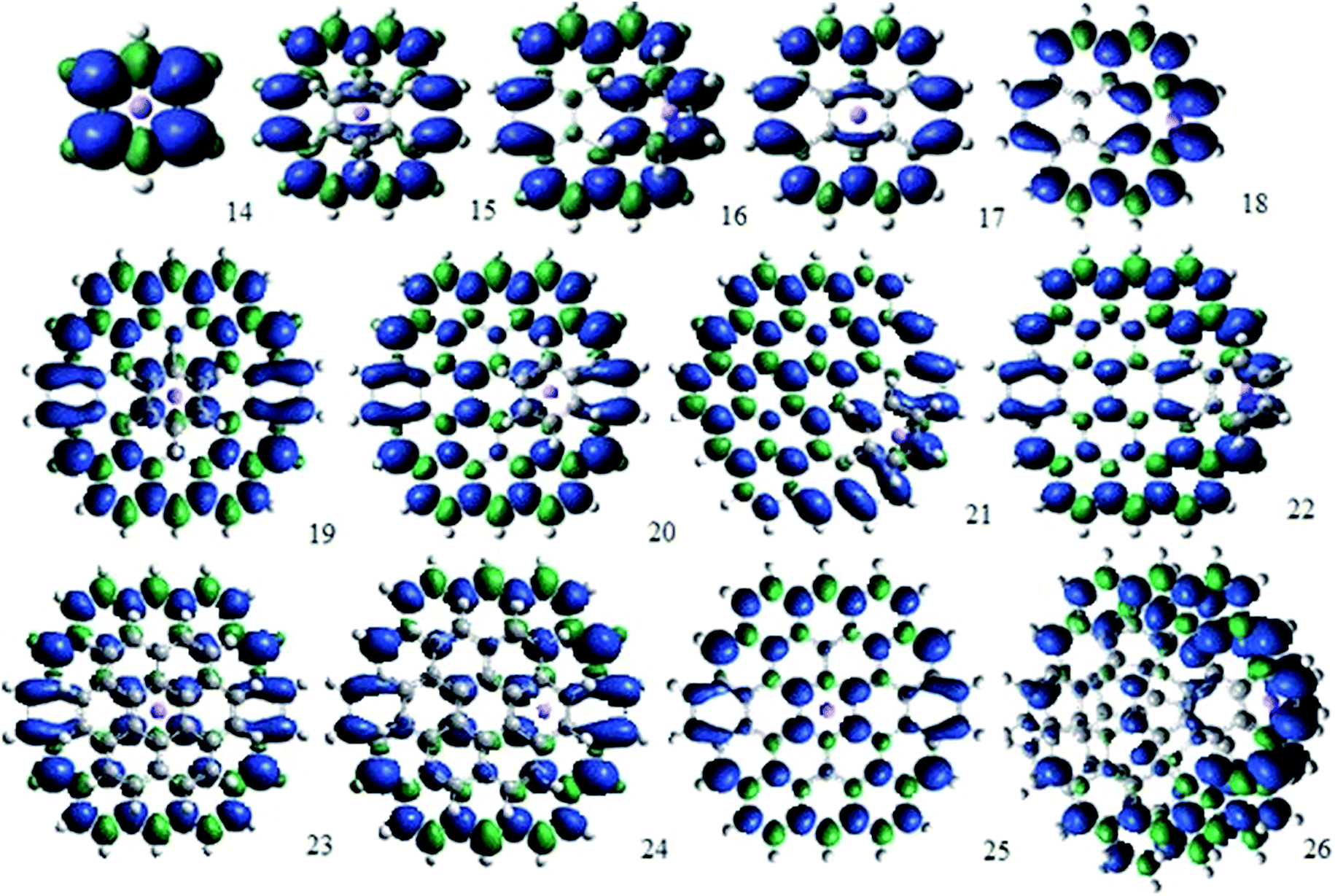 | ||
| Fig. 3 Studied bilayer GNFs. The isosurface value is ±0.0004 electrons per cubic atomic unit for positive values in blue and negative values in green. | ||
| No. | Adsorption energy (eV) | Spin-polarization (Mulliken atomic spin densities) | Alpha/beta gap (eV) |
|---|---|---|---|
| 14 | −0.027 | 0.22 | 1.32/5.86 |
| 15 | −0.034 | 0.28 | 0.73/3.28 |
| 16 | −0.039 | 0.23 | 1.1/3.67 |
| 17 | −0.033 | 0.14 | 0.82/3.54 |
| 18 | −0.043 | 0.13 | 0.87/3.57 |
| 19 | −0.050 | 0.20 | 0.79/2.62 |
| 20 | −0.049 | 0.24 | 0.82/2.62 |
| 21 | 1.444 | 0.29 | 0.91/2.67 |
| 22 | −0.053 | 0.29 | 0.95/2.65 |
| 23 | −0.043 | 0.20 | 0.64/2.49 |
| 24 | −0.047 | 0.25 | 0.61/2.47 |
| 25 | −0.046 | 0.10 | 0.61/2.51 |
| 26 | −0.046 | 0.15 | 0.60/2.59 |
The order of the flakes based on their stability is 21, 14, 17, 15, 16, 23, 18, 25, 26, 24, 20, 19 and 22. For relative stability, a particular rule has not been found. Unlike for single layers, the total number of C atoms is not a determining factor for the adsorption energy value. For instance, flake no. 22 has fewer C atoms relative to flakes no. 24 and no. 25, but its adsorption energy is red shifted. In contrast, flake no. 18, which has more C atoms relative to flakes no. 16 and no. 15, is more stable than both of those. However, between similar flakes, those which are doped by a Li atom and have the second layer nearer to the edge are steadier.
According to Table 2, between flakes 23 and 24, the latter whose Li atom is nearer to the edge is more stable; the same is true of flake no. 15 relative to 16, and no. 25 comparative to 26. Flake no. 22 is more stable than flake no. 20, and the adsorption energy of flake no. 20 is red shifted relative to flake no. 19. This is the same for flake no. 16 relative to flake no. 15. It is noteworthy that as the exception, flake no. 21 is not stable. For flake no. 21, the bilayer flake without dopant is more stable than the doped one, because the centre of each carbon ring is a stable position for the absorbent. In fact, the boundary H atoms of the smaller flake in both flakes no. 21 and 22 instead of a parallel position with respect to the larger flakes turn toward the larger flake centre. The only difference between these two flakes is that for flake no. 21, there is one H atom which stops this rotation. Meanwhile for flake no. 22, two boundary H atoms stop this rotation toward the larger flake centre. As a consequence, for flake no. 21, the optimized position of the smaller layer is perpendicular to the graphene flake and two boundary H atoms have been absorbed by two nearby benzene rings. As a result, the two H boundary atoms act similarly to two distinctive dopants themselves. Consequently this structure is more stable than the doped one in which there is one dopant for the same larger layer.
According to Table 2, the order of spin polarization amount according to the flake number is: 25, 18, 17, 26, 19, 23, 14, 16, 20, 24, 15, 22, and 21. In addition, the spin polarization intervals are generally smaller for bilayer GNFs relative to monolayer ones with a similar radius. For instance, for GNFs no. 16 to 26 the spin polarization is less than a similarly doped monolayer GNF. Furthermore, according to Fig. 3, in flake no. 14 with a Li atom between the two coupled benzene rings, both surfaces are ferromagnetically spin polarized and strongly correlated (Fig. 4). For flake no. 15, one layer is FM while the smaller layer does not have any spin polarization with 10−2 accuracy. Consequently, we have both FM and NM layers in flake no. 15.
 | ||
| Fig. 4 Side view of GNFs no. 14 and 18. As is visible in the right side of this picture (top and bottom), the spin density distribution for the two different layers has been entangled similar to a joint. The isosurface value is ±0.0004 electrons per cubic atomic unit. | ||
For flake no. 16, like no. 14, the two surfaces have a common spin density region (Fig. 4). This common joint between the two layers happens because of the high concentration of spin density at the edges. Flake number 17 has two similar flakes doped by one Li in the centre. The important note about this structure is a drastic reduction of the spin density relative to the similar monolayer flake. However, both layers are still FM. GNF no. 18 is similar to no. 17; a reduction of magnetization in the FM layers is noticeable.
In fact for all GNFs, both doped layers are FM, if it be spin polarized. According to Table 2 and Fig. 3, flake no. 22 is more spin polarized relative to flakes no. 19 to 21, and the same rule applies for flake no. 24 relative to 23; and flake no. 26 relative to no. 25. Consequently, the spin polarization is dependent on the second layer’s size and position. In detail, the edge adsorption for the second layer increases FM properties. However, according to Fig. 4 and Table 2 for small size flakes, no. 14, 16 and 18, this rule is not correct any more, because the increase of the spin distribution on the edge has entangled the two layers.
According to Table 2, there are two effective factors influencing bilayer GNFs gap values. First, the gap is generally red shifted by increasing the number of C atoms. For instance, between flakes no. 22 and 23, the gap of the second flake is red shifted, because it has more C atoms. The second factor which affects the gap is the second layer position. For instance, between flakes 19 to 22, the latter which has a benzene layer nearer to the edge has a larger gap, same about flake no. 15 and 16. However, a systematic relation between the Li position and the gap has not been found.
In addition, according to Fig. 3, similar to monolayer cases, if a Li atom is adsorbed beside two H atoms or if Li is on a symmetry line passing through such a ring, a tunnel of spin polarized density is visible in the SMM. Indeed, a tunnel of spin polarized regions happens in that vicinity.
Because of a strong concentration of spin up, benzene rings with two H atoms at the edge are the best regions for connection in a circuit.
Application
Suggestions for spin amplifiers
As mentioned earlier, Li-doped single layers are generally better FMs in comparison to bilayer graphene. Consequently, doped monolayer structures are better amplifiers. However, in bilayer GNFs, the second layer could be managed for appropriate ferromagnetism and spin polarization. Additionally, among all the bilayer flakes, those which have a higher adsorption energy and a large spin polarization are superior spin amplifiers. Consequently, the author suggests flakes 22 and 24 as spin amplifiers, because these flakes have a high spin density and relative stability. The spin polarization of these bilayer GNFs is also near to the similar monolayer GNFs.The effect of the temperature on the dopant, at room temperature (270 < T < 400 ![[thin space (1/6-em)]](https://www.rsc.org/images/entities/char_2009.gif) K), is that the Li atoms fall in the boundary condition.55 Moreover, based on previous research,52 the interlayer spaces are preferable for adsorption. In addition, the current research shows that structures with the benzene or a dopant at the edge are more stable. Consequently, the proposed flakes are stable up to room temperature and Li-doped GNFs are SMMs and room temperature spin amplifiers.
K), is that the Li atoms fall in the boundary condition.55 Moreover, based on previous research,52 the interlayer spaces are preferable for adsorption. In addition, the current research shows that structures with the benzene or a dopant at the edge are more stable. Consequently, the proposed flakes are stable up to room temperature and Li-doped GNFs are SMMs and room temperature spin amplifiers.
A bilayer GNF as an amplifier could act better at higher temperature. In fact, because of the migration of Li and benzene rings to the edge, the spin polarization and the stability of the GNFs increase generally. However, the study of managing edge states and adsorbent type to increase spin density and whether more odd numbers of Li atoms increase spin polarization needs more research.
Spintronic on/off switch based on a Li-doped bilayer
Molecular orbitals (MOs) are conduction channels for electrons.56 These channels can be obstructed (localized) or not (delocalized). They can also be occupied by electrons or not. Any factor which changes this occupation allows us to tailor the electrical behaviour of the molecule.54 A non-conducting channel is a localized MO, which cannot connect both ends of the molecule attached to metallic contacts. Furthermore, the shapes of frontier molecular orbitals explain qualitatively the conduction of electrons through molecules attached to macroscopic contacts.54 Based on this analysis, the author suggests a structure similar to Fig. 5 for applications in the field of single electron on/off switches. According to Fig. 5, Li-doped bilayer GNFs with layers of different sizes could act as a single electron on/off switch. In such a SMM, OMO and UMO concentration switches between layers. Such a switch of molecular orbitals happens because of the repulsive effect of the H atoms.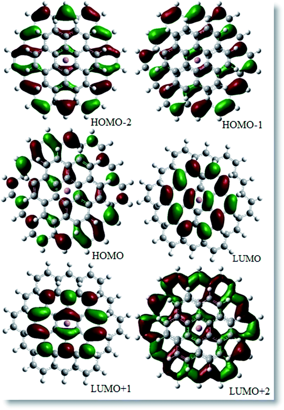 | ||
| Fig. 5 Spin up molecular orbitals view for bilayer GNF no. 17 which is a doped bilayer graphene with layers of different sizes. According to this figure, for HOMO−2 to LUMO+2, MOs are distributed on one layer. Colour code: red, positive; green, negative. The isovalue is 0.02. | ||
As determined previously, the stability and the spin polarization of these structures in comparison with other GNFs are high. In addition, for the proposed on/off switch for spintronic purposes, contacts should be added to one layer. Furthermore, based on Table 2 and Fig. 5, it is predictable that this type of switch will have a high on/off ratio, because of the low covering effects of two doped layers with different sizes. However, this ratio will be decreased by the movement of Li atoms to the edge of a SMM at higher temperatures (Fig. 3).
Memory devices based on a Li-doped bilayer
According to Fig. 5, when an electron transfers to the LUMO state of the depicted SMMs,56 there is no MO on the larger surface. This define a logical “0” state for a memory device. Moreover, when there is not any electron in the HOMO level, the probability of the existence of an electron in the smaller layer is zero. This effect defines a logical “1” digit. According to Fig. 5, for HOMO−2, HOMO−1, HOMO, LUMO, LUMO+1 and LUMO+2 such a switch of states also happens. Consequently, the switch between two layers and these up and down states can be used to define a memory device. Consequently, the author suggests the usage of a bilayer graphene SMM as a memory device, as well.Conclusion
All of the considered doped graphene structures with one Li atom are FMs, while a flake doped by two atoms is a NM which does not have any localized spin polarized state. This point makes it possible to build two FM and NM phases by the use of GNFs. Li-doped GNFs are spin polarized and the alpha and beta gaps are red shifted by increasing their size. Furthermore, Li-doped GNFs could be used as spintronic SMMs for room temperature applications, because these flakes generally have more stable edge states. For better conduction of spin polarized current, a contact group should be attached where two H atoms are bonded in a benzene ring. In addition, larger SMMs which have a dopant nearer to the boundary are better FMs. In flakes where the dopant is on a ring with two H atoms, spin amplifiers could act better. This point is a positive reason to propose the room temperature applications of doped GNFs as SMMs.For bilayer graphene, flakes of different sizes have been studied, where the dopant position and the second layer size and place are variable. Concerning the relative stability, flakes with the adsorbent nearer to the edge are more stable. Spin polarization is also dependent on the second layer size and position. Both layers are FM, if it be spin polarized. Additionally, the edge adsorption of the second layer increases the FM properties. Furthermore, where the two layers are small, because of the high intensity of the spin distribution on the edge, the two layers are entangled in each other and spin polarization decreases drastically. Moreover, for bilayer SMMs, the alpha and beta gaps are generally red shifted by the increase of the number of C atoms. In addition, those benzene rings with two H atoms at the edge are the best choices to be used as the contact group in a circuit.
For spintronic purposes, the proposed SMMs could be used as spin amplifiers, spin on/off switches and memory devices for room temperature applications. Monolayer Li-doped flakes are better FMs and also amplifiers. Graphene flakes similar to flakes no. 22 and 24 have high spin density and relative stability; thus, those flakes are better spin amplifiers. In addition, bilayer flakes with layers of different sizes could act as an on/off switch and an amplifier, as well. In addition, in these flakes, the spin polarized MO switches between layers. According to the switch of MOs, logical “0” and “1” states for molecular memory devices could be achievable.
Acknowledgements
This work was made possible by the facilities of Computational Nanotechnology Supercomputing Centre, Institute for Research in Fundamental Science (IPM). The author is immensely grateful to Dr Edward McCann for his precious comments on an earlier version of the manuscript.References
- S. Datta, Quantum transport: atom to transistor, Cambridge University Press, 2005 Search PubMed.
- G. Yin, et al., Polarization-induced switching effect in graphene nanoribbon edge-defect junction, J. Chem. Phys., 2009, 131(23), 234706 CrossRef CAS PubMed.
- M. N. Leuenberger and D. Loss, Quantum computing in molecular magnets, Nature, 2001, 410(6830), 789–793 CrossRef CAS PubMed.
- L. Bogani and W. Wernsdorfer, Molecular spintronics using single-molecule magnets, Nat. Mater., 2008, 7(3), 179–186 CrossRef CAS PubMed.
- W. Wernsdorfer, Molecular magnets: a long-lasting phase, Nat. Mater., 2007, 6(3), 174–176 CrossRef CAS PubMed.
- G. Christou, et al., Single-molecule magnets, MRS Bull., 2000, 25(11), 66–71 CrossRef CAS.
- D. Gatteschi, R. Sessoli and J. Villain, Molecular nanomagnets, Oxford University Press, 2006 Search PubMed.
- C. Timm and F. Elste, Spin amplification, reading, and writing in transport through anisotropic magnetic molecules, Phys. Rev. B: Condens. Matter Mater. Phys., 2006, 73(23), 235304 CrossRef.
- F. Elste and C. Timm, Transport through anisotropic magnetic molecules with partially ferromagnetic leads: spin-charge conversion and negative differential conductance, Phys. Rev. B: Condens. Matter Mater. Phys., 2006, 73(23), 235305 CrossRef.
- J. E. Green, et al., A 160 kilobit molecular electronic memory patterned at 1011 bits per square centimetre, Nature, 2007, 445(7126), 414–417 CrossRef CAS PubMed.
- M. Drögeler, et al., Nanosecond spin lifetimes in single- and few-layer graphene–hBN heterostructures at room temperature, Nano Lett., 2014, 14(11), 6050–6055 CrossRef PubMed.
- M. Drögeler, et al., Nanosecond spin lifetimes in bottom-up fabricated bilayer graphene spin-valves with atomic layer deposited Al2O3 spin injection and detection barriers, 2015, arXiv preprint arXiv:1507.02677.
- F. Volmer, et al., Spin and charge transport in graphene-based spin transport devices with Co/MgO spin injection and spin detection electrodes, 2015, arXiv preprint arXiv:1503.01735.
- W. L. Wang, S. Meng and E. Kaxiras, Graphene nanoflakes with large spin, Nano Lett., 2008, 8(1), 241–245 CrossRef CAS PubMed.
- N. Kheirabadi, A. Shafiekhani and M. Fathipour, Review on graphene spintronic, new land for discovery, Superlattices Microstruct., 2014, 74, 123–145 CrossRef CAS.
- Y. R. Kim, et al., Electrostatically transparent graphene quantum-dot trap layers for efficient nonvolatile memory, Appl. Phys. Lett., 2015, 106(10), 103105 CrossRef.
- I. Beljakov, et al., Spin-crossover and massive anisotropy switching of 5d transition metal atoms on graphene nanoflakes, Nano Lett., 2014, 14(6), 3364–3368 CrossRef CAS PubMed.
- M. Droth and G. Burkard, Spintronics with graphene quantum dots, Phys. Status Solidi RRL, 2015, 9999 Search PubMed.
- G. Konstantatos, et al., Hybrid graphene-quantum dot phototransistors with ultrahigh gain, Nat. Nanotechnol., 2012, 7(6), 363–368 CrossRef CAS PubMed.
- J. Güttinger, et al., Spin states in graphene quantum dots, Phys. Rev. Lett., 2010, 105(11), 116801 CrossRef PubMed.
- C. Volk, et al., Electronic excited states in bilayer graphene double quantum dots, Nano Lett., 2011, 11(9), 3581–3586 CrossRef CAS PubMed.
- P. Potasz, et al., Electronic properties of gated triangular graphene quantum dots: magnetism, correlations, and geometrical effects, Phys. Rev. B: Condens. Matter Mater. Phys., 2012, 85(7), 075431 CrossRef.
- A. Jacobsen, et al., Transport in a three-terminal graphene quantum dot in the multi-level regime, New J. Phys., 2012, 14(2), 023052 CrossRef.
- J. Güttinger, et al., Transport through graphene quantum dots, Rep. Prog. Phys., 2012, 75(12), 126502 CrossRef PubMed.
- D. Bischoff, et al., Electronic triple-dot transport through a bilayer graphene island with ultrasmall constrictions, New J. Phys., 2013, 15(8), 083029 CrossRef.
- C. Beenakker, Colloquium: Andreev reflection and Klein tunneling in graphene, Rev. Mod. Phys., 2008, 80(4), 1337 CrossRef CAS.
- C. Stampfer, et al., Tunable graphene single electron transistor, Nano Lett., 2008, 8(8), 2378–2383 CrossRef CAS PubMed.
- J. Lu, et al., Transforming C60 molecules into graphene quantum dots, Nat. Nanotechnol., 2011, 6(4), 247–252 CrossRef CAS PubMed.
- L. Cancado, et al., Influence of the atomic structure on the Raman spectra of graphite edges, Phys. Rev. Lett., 2004, 93(24), 247401 CrossRef CAS PubMed.
- A. Affoune, et al., Experimental evidence of a single nano-graphene, Chem. Phys. Lett., 2001, 348(1), 17–20 CrossRef CAS.
- A. Affoune, et al., Electrophoretic deposition of nanosized diamond particles, Langmuir, 2001, 17(2), 547–551 CrossRef CAS.
- D. V. Kosynkin, et al., Longitudinal unzipping of carbon nanotubes to form graphene nanoribbons, Nature, 2009, 458(7240), 872–876 CrossRef CAS PubMed.
- A. Müller, et al., Bilayer graphene quantum dot defined by topgates, J. Appl. Phys., 2014, 115(23), 233710 CrossRef.
- Y. Zhou, et al., Epitaxial Growth of Asymmetrically-Doped Bilayer Graphene for Photocurrent Generation, Small, 2014, 10(11), 2245–2250 CrossRef CAS PubMed.
- S. Fringes, et al., Charge detection in a bilayer graphene quantum dot, Phys. Status Solidi B, 2011, 248(11), 2684–2687 CrossRef CAS.
- S. Schnez, et al., Observation of excited states in a graphene quantum dot, Appl. Phys. Lett., 2009, 94(1), 012107 CrossRef.
- F. Molitor, et al., Observation of excited states in a graphene double quantum dot, EPL, 2010, 89(6), 67005 CrossRef.
- F. J. Owens, Electronic and magnetic properties of armchair and zigzag graphene nanoribbons, J. Chem. Phys., 2008, 128(19), 194701 CrossRef PubMed.
- B. Huang, et al., Towards graphene nanoribbon-based electronics, Front. Phys. China, 2009, 4, 269–279 CrossRef.
- Y.-W. Son, M. L. Cohen and S. G. Louie, Energy gaps in graphene nanoribbons, Phys. Rev. Lett., 2006, 97(21), 216803 CrossRef PubMed.
- O. Hod, V. Barone and G. E. Scuseria, Half-metallic graphene nanodots: a comprehensive first-principles theoretical study, Phys. Rev. B: Condens. Matter Mater. Phys., 2008, 77(3), 035411 CrossRef.
- Y.-W. Son, M. L. Cohen and S. G. Louie, Half-metallic graphene nanoribbons, Nature, 2006, 444(7117), 347–349 CrossRef CAS PubMed.
- W. L. Wang, et al., Topological frustration in graphene nanoflakes: magnetic order and spin logic devices, Phys. Rev. Lett., 2009, 102(15), 157201 CrossRef PubMed.
- W. Pisula, X. Feng and K. Müllen, Charge-Carrier Transporting Graphene-Type Molecules, Chem. Mater., 2010, 23(3), 554–567 CrossRef.
- N. Emery, et al., Superconductivity of bulk CaC6, Phys. Rev. Lett., 2005, 95(8), 087003 CrossRef CAS PubMed.
- D. Guzman, H. Alyahyaei and R. Jishi, Superconductivity in graphene–lithium, 2D Mater., 2014, 1(2), 021005 CrossRef.
- B. M. Ludbrook, G. Levy, P. Nigge, M. Zonno and M. Schneider, et al., Evidence for superconductivity in Li-decorated monolayer graphene, Proc. Natl. Acad. Sci. U. S. A., 2015, 112, 11795–11799 CrossRef CAS PubMed.
- A. D. Becke, Density-functional thermochemistry. III. The role of exact exchange, J. Chem. Phys., 1993, 98(7), 5648–5652 CrossRef CAS.
- C. Lee, W. Yang and R. G. Parr, Development of the Colle–Salvetti correlation-energy formula into a functional of the electron density, Phys. Rev. B: Condens. Matter Mater. Phys., 1988, 37(2), 785 CrossRef CAS.
- M. J. Frisch, G. W. Trucks, H. B. Schlegel, G. E. Scuseria, M. A. Rob, J. R. Cheeseman, J. A. Montgomery Jr, T. Vreven, K. N. Kudin, J. C. Burant, J. M. Millam, S. S. Iyengar, J. Tomasi, V. Barone, B. Mennucci, M. Cossi, G. Scalmani, N. Rega, G. A. Petersson, H. Nakatsuji, M. Hada, M. Ehara, K. Toyota, R. Fukuda, J. Hasegawa, M. Ishida, T. Nakajima, Y. Honda, O. Kitao, H. Nakai, M. Klene, X. Li, J. E. Knox, H. P. Hratchian, J. B. Cross, V. Bakken, C. Adamo, J. Jaramillo, R. Gomperts, R. E. Stratmann, O. Yazyev, A. J. Austin, R. Cammi, C. Pomelli, J. W. Ochterski, P. Y. Ayala, K. Morokuma, G. A. Voth, P. Salvador, J. J. Dannenberg, V. G. Zakrzewski, S. Dapprich, A. D. Daniels, M. C. Strain, O. Farkas, D. K. Malick, A. D. Rabuck, K. Raghavachari, J. B. Foresman, J. V. Ortiz, Q. Cui, A. G. Baboul, S. Clifford, J. Cioslowski, B. B. Stefanov, G. Liu, A. Liashenko, P. Piskorz, I. Komaromi, R. L. Martin, D. J. Fox, T. Keith, M. A. Al-Laham, C. Y. Peng, A. Nanayakkara, M. Challacombe, P. M. W. Gill, B. Johnson, W. Chen, M. W. Wong, C. Gonzalez and J. A. Pople, Gaussian 03, Gaussian, Inc, Wallingford, CT, 2003 Search PubMed.
- N. Kheirabadi and A. Shafiekhani, The ground state of graphene and graphene disordered by vacancies, Phys. E, 2013, 47, 309–315 CrossRef CAS.
- N. Kheirabadi and A. Shafiekhani, Graphene/Li-ion battery, J. Appl. Phys., 2012, 112(12), 124323 CrossRef.
- A. I. Liechtenstein, et al., Local spin density functional approach to the theory of exchange interactions in ferromagnetic metals and alloys, J. Magn. Magn. Mater., 1987, 67(1), 65–74 CrossRef CAS.
- J. M. Seminario, A. G. Zacarias and P. A. Derosa, Theoretical analysis of complementary molecular memory devices, J. Phys. Chem. A, 2001, 105(5), 791–795 CrossRef CAS.
- H. Tachikawa and A. Shimizu, Diffusion dynamics of the Li atom on amorphous carbon: a direct molecular orbital–molecular dynamics study, J. Phys. Chem. B, 2006, 110(41), 20445–20450 CrossRef CAS PubMed.
- F. Bonaccorso, et al., Graphene photonics and optoelectronics, Nat. Photonics, 2010, 4(9), 611–622 CrossRef CAS.
| This journal is © The Royal Society of Chemistry 2016 |