
Synthesis and applications of large-area single-layer graphene
Xiao-Hong Lin
and
Jing-Gang Gai
*
State Key Laboratory of Polymer Materials Engineering, Polymer Research Institute of Sichuan University, Chengdu, Sichuan 610065, China. E-mail: gaijinggang@scu.edu.cn; Fax: +86 28 85402465; Tel: +86 28 85467166
First published on 4th February 2016
Abstract
Large-area graphene is gaining heightened attention in the fields of optoelectronics and highly selective membrane separation due to its unique physicochemical properties including exceptionally high surface, electro mobility, thermal conductivity, mechanical strength, and one atom thickness. These outstanding properties can lead to novel or improved technologies to address the pressing global challenges in transparent conducting electrodes, transistors, ultrathin electromagnetic shielding film, osmotic energy production, highly selective single molecule gas detection, desalination, DNA sequencing, etc. This review assesses the progress in two categories of methods for preparing large-area graphene, namely chemical assembly of small graphene sheets and chemical vapor deposition method. We also discuss the challenges for preparing large-area graphene with high qualities and controllable layers and for transferring graphene film to various substrates with large area, clean, and low defect surface. Applications of large-area graphene in the optoelectronics fields have been discussed by Bonaccorso et al. We mainly discuss its applications in highly selective membrane separation including single molecule gas detection, desalination, DNA sequencing and osmotic energy production. Finally, we outline the global investment and industrial production of large-area graphene.
 Xiao-Hong Lin | Xiao-Hong Lin received her bachelor's degree in Polymer Science and Engineering from Qilu University of Technology, China. She is now studying for a master's degree in Materials Science, Sichuan University, China. Her research focuses on seawater desalination using nanoporous graphene membrane. |
 Jing-Gang Gai | Jing-Gang Gai is an associate professor at the State Key Laboratory of Polymer Materials Engineering, Polymer Research Institute of Sichuan University, China. He received his MS degree from Sichuan University in 2005, and his Ph.D. from Institut National Polytechnique de Lorraine, France in 2009. His research interests are in the areas of angstrom film and its applications in membrane separations and energy production by osmotic energy. |
1. Introduction
Graphene is composed of a single layer of carbon atoms which pack into a two-dimensional (2D) honeycomb lattice.1,2 It is the basic building block for graphitic materials of other dimensionalities including 0D fullerenes,3 1D nanotubes4–8 and 3D graphite. More and more scientists have engaged in researches related with graphene since Geim and Novoselov successfully isolated pristine graphene utilizing the adhesive tape.9Graphene exhibited many excellent properties10–13 including mechanical,14 thermal,15 chemical,16,17 optical,18 electrical properties.19 The strength of defect-free single crystalline graphene is the highest among the materials which have been tested. It is up to 130 GPa which is 100 times higher than that of the steel.14 The thermal conductivity is about 5000 W m−1 K−1 and is 3 times higher than that of diamond.15 The intrinsic mobility is up to 2 × 105 cm2 V−1 s−1 which is 10 times higher than that of commercial silicon.19 Besides, the theoretical thickness of single layer graphene is only 0.34 nm, and it is the thinnest 2D material up till now.1
Chemically doped graphene, especially nitrogen-doped and boron-doped graphene, also has excellent properties and it has been widely studied. Pristine single-layer graphene is a gapless material, but the creation of band gap is necessary for many applications in energy related devices. Chemical doping of graphene can produce a band gap and it can lead to useful properties as well. Rao et al. systematically reviewed the synthesis, characterization, properties and applications of graphene doped with nitrogen, boron and other elements.20 For nitrogen-doped graphene, the nitrogen source is usually ammonia and the nitrogen content can be varied from 0.25 to 15 at% through different synthetic methods. For boron-doped graphene, the boron source can be B2H6, H3BO3, B2O3, BCl3 or BF3 and the boron content can be varied from 0.22 to 3 at%. These synthetic methods of doped graphene mainly include arc-discharge, CVD, ball milling, thermal treatment and microwave treatment. Among them, arc discharge is a facile, low-cost and efficient method and it's versatile for producing various carbon nanomaterials.21–25 Compared with pure graphene, optical, magnetic and electrical properties of doped graphene have great changes. For example, the photoluminescence emission of nitrogen-doped graphene is significantly enhanced. These changes are mainly associated with the change of the electronic structure of graphene. Due to its excellent performance, chemically doped graphene has a wide range of applications including supercapacitors, adsorption of gases, lithium ion batteries, field emission, water splitting and so on. For instance, the capacitance of nitrogen-doped graphene prepared under plasma conditions is 4 times higher than that of pristine graphene.
Due to these excellent properties mentioned above, scientists always pursue the defect-free large-area graphene (LAG). In these years, the preparation technologies and the applications of LAG have developed rapidly, especially in Korea, United States, Japan and China. LAG has been used to address the pressing global challenges of transparent conducting electrodes, field effect transistors, flexible and wearable touch screen and display, ultrathin electromagnetic shielding film, highly selective molecular sieve membranes for single molecule gas detection, desalination, DNA sequencing and osmotic energy production. Since 2004, the number of academic papers related to LAG has significantly increased. Fig. 1 illustrates the number of graphene-related and LAG-related academic papers in recent years. There were nearly 16![[thin space (1/6-em)]](https://www.rsc.org/images/entities/char_2009.gif) 000 papers published with the keyword “graphene” and about 600 papers published with the keyword “LAG” in 2014 (Web of Science).26
000 papers published with the keyword “graphene” and about 600 papers published with the keyword “LAG” in 2014 (Web of Science).26
 | ||
| Fig. 1 The number of published academic papers about graphene (left) and large-area graphene (right) in different years. | ||
Some representative works are listed in what follows chronologically. In 2006, for the first time, Somani et al. experimentally demonstrated that few layers of planar nano-graphenes (PFLGs) could be directly synthesized by simple thermal CVD method.27 They scraped the graphene grown on Ni sheets (2 × 2 cm2) off using a sharp blade and collected the powder. They observed that the graphitic structure includes about 35 layers of graphene (Fig. 2a). In 2007, Obraztsov et al. adopted CVD method to prepare large area graphitic films with 3 to 6 graphene layers.28 They used silicon and nickel square plates with lateral dimensions of 10 × 10 mm2 or 25 × 25 mm2 as substrates. There are obvious differences between the morphologies of films deposited on Ni and Si substrates (Fig. 2b). In 2008, Eda et al. reported a solution-based method (vacuum filtration method) of preparing large-area reduced graphene oxide (RGO), using which they successfully fabricated a 10 cm2 RGO membrane with 1–5 layers of graphene (Fig. 2c).29 In June 2009, Li et al. successfully prepared large area, high quality and uniform graphene films on copper substrates adopting CVD method. More than 95% of the 1 × 1 cm2 film was monolayer graphene, 3–4% was bilayer graphene and the rest small fraction (<1%) was trilayer or few-layer (<10 layers) graphene (Fig. 2d).30 They found that the graphene grew on copper by a surface-catalyzed process. Then in August, Li et al. showed a photograph of a 4.5 × 4.5 cm2 graphene on quartz substrate (Fig. 2e) fabricated by CVD method and also reported an improved method to transfer graphene to other substrates with much lower densities of cracks and tears.31
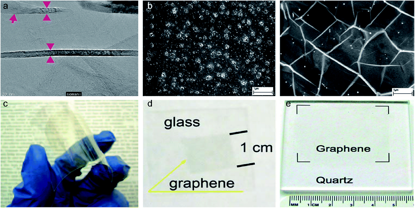 | ||
| Fig. 2 Representative pictures about large-area graphene before 2010. (a) HR-TEM image of PFLG film which shows graphitic structure marked by two arrows (ref. 27). (b) The SEM images of graphene films grown on Si (left) and Ni (right) respectively (ref. 28). (c) Photograph of 10 cm2 GO thin films on plastic substrate (ref. 29). (d) Graphene film transferred onto a glass plate, more than 95% of the 1 × 1 cm2 film is monolayer graphene (ref. 30). (e) 4.5 × 4.5 cm2 graphene on quartz substrate (ref. 31). | ||
As can be seen from Fig. 1, the researches about LAG have increased rapidly since 2010. There was a major breakthrough in the preparation of LAG in 2010. Bae et al. from Sungkynkwan University of Korea first reported a roll-to-roll (R2R) method to produce LAG films.32,33 They adopted the CVD method to prepare LAG on flexible ultra-large copper substrates. The films were 30-inch in the diagonal direction (Fig. 3a) and were predominantly monolayer. The films can be transferred to a target substrate by R2R method.
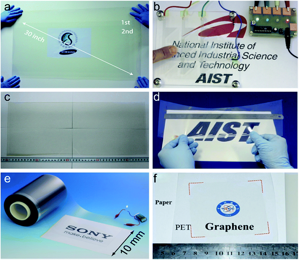 | ||
| Fig. 3 Representative pictures about large-area graphene after 2010. (a) A transparent ultralarge-area graphene film transferred on a 35-inch PET sheet (ref. 32). (b) A fabricated touch panel using the graphene-based transparent conductive films (ref. 34). (c) Photograph of 20 × 47 cm2 GO film deposited directly on a PET substrate by rod coating method (ref. 35). (d) A graphene film in area of 294 × 100 mm2 transferred onto PET substrate (ref. 36). (e) A 100 m-long, 230 mm-wide graphene film (ref. 37). (f) Photograph of 7 × 7 cm2 monolayer graphene film (ref. 38). | ||
In 2011, Kim et al. developed a large-area surface wave plasma (SWP) CVD apparatus to fabricate LAG-based films consisting of few-layer graphene sheets at lower temperatures (300–400 °C).34 The graphene film with lateral dimensions of 23 × 20 cm2 exhibited excellent optical and electrical properties, and has been successfully applied in the preparations of touch panel (Fig. 3b). Then in 2012, Wang et al. reported a novel method—rod coating to produce large-scale, transparent and conductive RGO films.35 This method can be carried out on arbitrary substrates at room temperature. They showed a graphene oxide (GO) film (20 × 47 cm2) deposited directly on a poly(ethylene terephthalate) (PET) substrate (Fig. 3c) and the RGO/PET film was successfully used in electrode.
Yamada et al. established a R2R microwave plasma (MWP) CVD process to prepare LAG films at low temperature.36 They deposited a graphene film with an area of 294 × 100 mm2 on Cu substrate and then transferred to PET film (Fig. 3d) below 400 °C. In 2013, Kobayashi et al. from Sony Corporation reported a new method—R2R CVD which applied selective Joule heating of the copper foil to achieve low pressure thermal CVD synthesis and a direct R2R transfer process, successfully producing a 100 m-long, 230 mm-wide high-quality graphene film which was predominantly composed of single-layer graphene (Fig. 3e).37
In 2014, Liu et al. reported an effective way by using CVD method to synthesize high-quality and uniform monolayer graphene without bilayer regions.38 They fabricated a 7 × 7 cm2 monolayer graphene (Fig. 3f). Ryu et al. adopted a method of hydrogen-free rapid thermal chemical vapor deposition (RT-CVD) to produce LAG films. They got homogeneous 400 × 300 mm2 graphene films,39 which was successfully used to fabricate a capacitive multitouch device and to install a mobile phone (Fig. 11d). More details are shown in Table 1.
| Year | Synthesis method | Size/cm2 | Layer number | Properties | Applications | Reference |
|---|---|---|---|---|---|---|
| 2006 | CVD | 2 × 2 (Ni) | ∼20–35 | — | — | 27 |
| 2007 | CVD | 2.5 × 2.5 (Ni) | 3–6 | — | — | 28 |
| 2008 | Vacuum filtration | 10 | 1–5 | Exist structural defects, lowest sheet resistance: ∼43 kΩ sq−1, transparency: 60–95%, electron mobility: ∼0.2 cm2 V−1 s−1 | Thin-film transistors (TFTs) | 29 |
| 2009 | CVD | 1 × 1 (Cu) | 1 (>95%) | Monolayer >95%, electron mobility: ∼4050 cm2 V−1 s−1 | Field-effect transistors | 30 |
| CVD | 4.5 × 4.5 | Excellent mechanical stability, sheet resistance: ∼350 Ω sq−1, transmittance: 86–98% | Transparent conductive electrode | 31 | ||
| 2010 | CVD | 30-inch (Cu) | Monolayer (mostly) | Sheet resistance: ∼125 Ω sq−1, optical transmittance: 97.4%, half-inter quantum Hall effect | Transparent electrode | 32 |
| 2011 | SWP-CVD | 23 × 20 (Cu) | Few-layer | Sheet resistance: 2.2–45 kΩ sq−1, optical transmittance: 78–94% (on glass plate) | Capacitive touch panel | 34 |
| 2012 | Rod-coating | 20 × 47 (PET) | 1–4, >4 (can be tuned) | Sheet resistance: 1.68–20.1 kΩ sq−1, optical transmittance: 64.6–92.6%, excellent foldability and uniformity | Touch screen | 35 |
| MWP CVD | 29.4 × 10 (Cu) | 1–4 | Optical transmittance: 95%, sheet resistance: 0.1–7 × 10⁵ Ω sq−1 | Electronic devices | 36 | |
| 2013 | R2R CVD | 100 m × 23 cm (Cu) | Monolayer (mostly) | Coverage rate: 89–98%, sheet resistance: ∼150 Ω sq−1, carrier mobility: ∼900 cm2 V−1 s−1 | — | 37 |
| 2014 | CVD | 7 × 7 (Cu) | Monolayer | Hole mobility 2534.3 ± 97.6 cm2 V−1 s−1, high uniformity | — | 38 |
| RT-CVD | 40 × 30 (Cu) | — | Sheet resistance: 249 ± 17 Ω sq−1 | Touch screen | 39 |
This review first discusses the preparation of LAG films. There are mainly two kinds of methods including chemical assembly of small graphene sheets and CVD method. Then, we summarize the applications of graphene films in membrane separation including gas separation, water desalination and DNA sequencing. Thirdly, we introduce the global investment in the field of graphene and the industrial production of graphene films. Finally, we will highlight challenges that should be overcome in order to achieve pervasive application of LAG films.
2. Preparation
There have been many methods for the preparation of graphene, for instance, Rao et al. summarized various synthetic methods of different layers of graphene.13 Up to now, chemical assembly of small graphene sheets12,33,40 and CVD method are two principal methods for the preparation of LAG.32,37,41 These two methods are emphatically discussed in this review.2.1. Chemical assembly
Chemical assembly is a solution-processing procedure of graphene or graphene oxide dispersed in a solvent. The resulting solution can be directly deposited on any substrates via the following methods: rod-coating,35,42–45 spin-coating of RGO,46–52 dip-coating of GO,53–56 vacuum filtration of GO suspension,29,57–68 interfacial assembly,69–71 spray coating72–80 and so forth.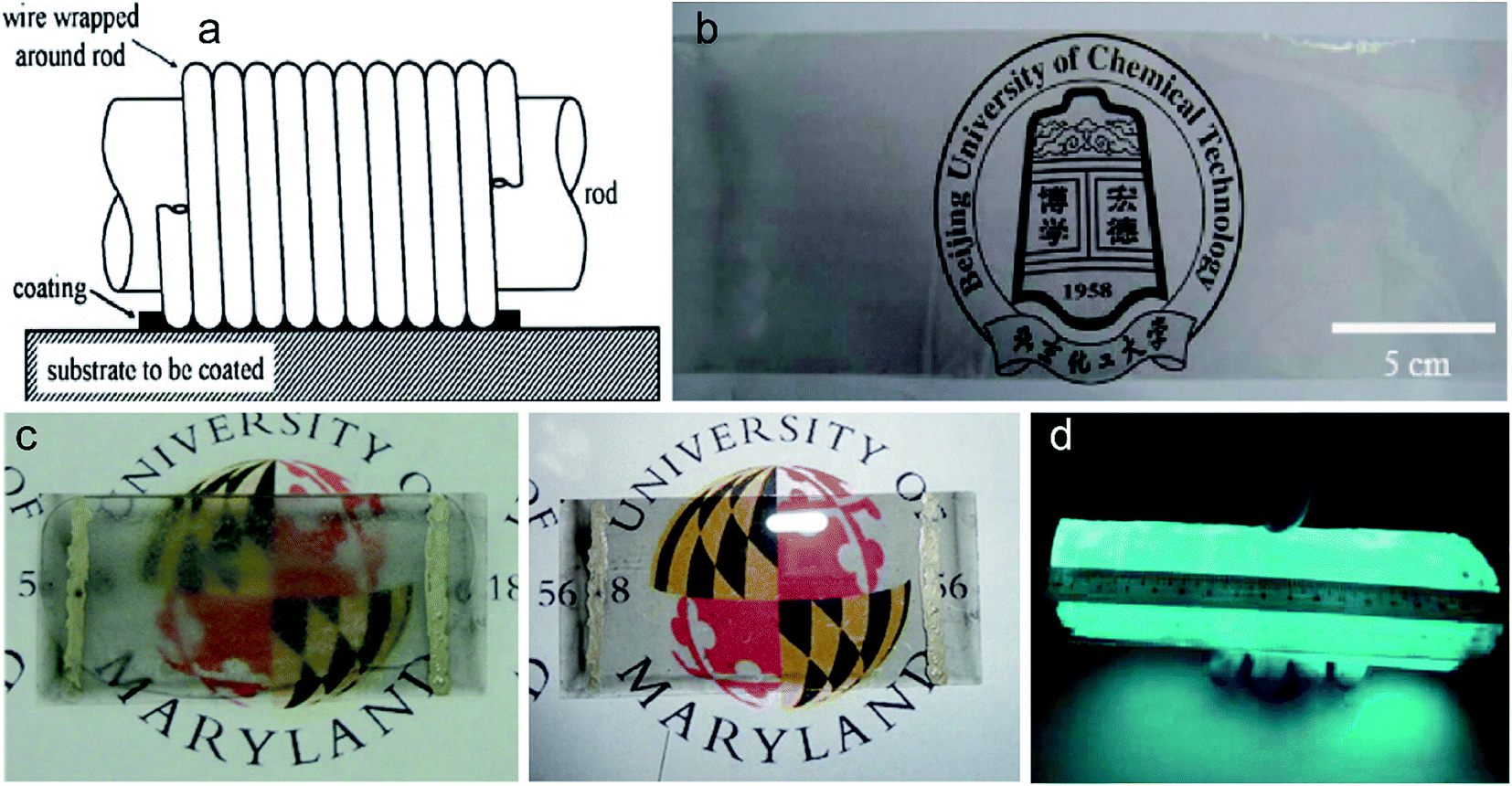 | ||
| Fig. 4 (a) Schematic diagram of rod coating method (ref. 45). (b) 25 × 10 cm2 SWNT thin film on a PET substrate with good transparency (ref. 44). (c) RGO film coated glass showed excellent defrosting performance (ref. 43). (d) A 14 × 18 cm2 AC LED device which worked perfectly under the bending state (ref. 42). | ||
In general, the GO solution is used as a coating material followed by reduction treatment. The obtained RGO thin film is often used to fabricate conductive and transparent electrodes. In 2012, for the first time, Wang et al. combined rod coating and room-temperature reduction of GO to fabricate a large area (20 × 47 cm2) RGO film on flexible PET substrate.35 In the experiment, the concentration of GO solution was 0.05–2.5 mg mL−1 and the wire diameter of the rod was 0.2 mm. With the increase of GO concentration from 0.5 to 2.5 mg mL−1, the transmittance and sheet resistance of RGO films decreased from 92.6% to 64.6% and 20.1 to 1.68 kΩ sq−1, respectively. The room-temperature reduction of GO reduces the consumption of energy, but the use of palladium catalyst increases the cost and the pressurized hydrogen in autoclave may induce safety problems.
In the same year, Xie et al. invented a wormlike micelle assisted rod coating method to prepare transparent and conductive thin films on flexible plastics.44 They selected a cetyltrimethylammonium hydroxide/p-toluenesulfonic acid wormlike micelle system for the dispersion of different nanomaterials. The system can also adjust the viscosity of nanomaterial solution. They chose single-walled carbon nanotubes (SWNTs) as experimental model, successfully preparing a 25 × 10 cm2 SWNT thin film on PET substrate with good transparency (Fig. 4b). After doping in thionyl chloride solution, the transmittance of SWNT thin films was about 78% and the sheet resistance was as low as 480 Ω sq−1. This method can be applied to various nanomaterials and their hybrids, such as, CNTs, RGO and silver nanowires. However, the complete removal of residual surfactant which will influence the sheet resistance is difficult and complex.
In 2014, Wang et al. adopted Meyer-rod coating method followed by thermal reduction process to prepare RGO thin films on flexible glass.43 They got a conductive RGO film on 10 × 20 cm2 flexible glass substrate with transmittance over 40% and sheet resistance of ∼5 × 10³ Ω sq−1. The RGO thin films can be used as heaters due to its high electrical conductivity. The conductive RGO thin films can be used to make defrost glasses for vehicle windows. Wang et al. added an electrode pair (Ag) on RGO film/flexible glass and observed that frost on the flexible glass was eliminated when 10 volts was applied to it (Fig. 4c). Yang et al. employed rod coating method to fabricate light-emitting diodes (LED) with double functional GO-based flexible alternating current (AC).42 In the experiment, GO film was used as dielectric layer and RGO film was used as conductive electrode. The sheet resistance of RGO film can be as low as 2.6 kΩ sq−1 at the transmittance of 69%. They successfully fabricated a 14 × 18 cm2 AC LED device (Fig. 4d) and the luminance of the device increased steadily with the rise of frequency due to low dielectric loss property of GO.
The rod coating method for the preparation of LAG has many advantages including low cost, easy to operate, scalable, and precise in thickness control (by adjusting the solution concentration or the diameter of rod wire). It can also operate directly on any substrates at room temperature. But the viscosity of the solution should not be too high, or it will reduce the flowability of the fluid between the wire windings. For this method, the optimum viscosity range of coating solution is 0.02–1.00 Pa s.44 From what has been discussed above, we found that LAG films prepared by rod-coating method have good transparency and conductivity. Therefore, the industrial production of transparent and conductive thin films may be achieved through the combination of rod coating and R2R technology.
 | ||
| Fig. 5 (a) Schematic diagram of spin coating method (ref. 47). (b) A 300 mm, transparent and flexible graphene film transferred onto PET film (ref. 50). (c) Graphene composite electrode on PET (ref. 52). | ||
In 2008, Robinson et al. reported a modified spin coating method—blowing dry N2 in the spin-coating process (Fig. 5a).47 It can accelerate the evaporation of solvent, thereby increasing the interaction between GO sheets and the substrate to obtain a continuous film. LAG film can also be obtained by spin coating method. Yamaguchi et al. prepared 300 mm wafer-scale, highly uniform and transparent GO films with controllable number of layers (Fig. 5b) by modified spin coating method.50 The sheet resistance and transmittance of 15 nm thin film were ∼1 kΩ sq−1 and ∼70%. For the first time, Chang et al. fabricated a new type of graphene composite electrode in 2010.52 The GO solution was prepared by surfactant-assisted exfoliation of graphite oxide followed by in situ chemical reduction. The graphene composite electrode was got by spin coating of the mixture of RGO solution and poly(3,4-ethylenedioxythiophene): poly(styrenesulfonate) (PEDOT:PSS) without further processing (Fig. 5c). This graphene composite electrode exhibited high mechanical and electrical stability in bending tests of at least 1000 cycles. The films prepared by spin coating method are generally uniform and continuous, while the reduction of GO is usually incomplete and the reduction process is complex. The reduction of GO often requires high temperature annealing or the use of toxic hydrazine as reductant. In addition, spin motion can cause stress and a large amount of solution will be wasted in the spin-coating process.
Dip coating is a direct and effective method, and it has the following advantages: low cost, easy to operate, continuous and large area production can be achieved through mechanization or automation. The thickness of GO films can be adjusted by changing the concentration of GO suspension, immersion time of substrates in GO solution and the number of coating cycles, but the resulting films are generally nonuniform due to aggregation of GO sheets. After thermal reduction, nonuniformity of the film thickness can be improved.
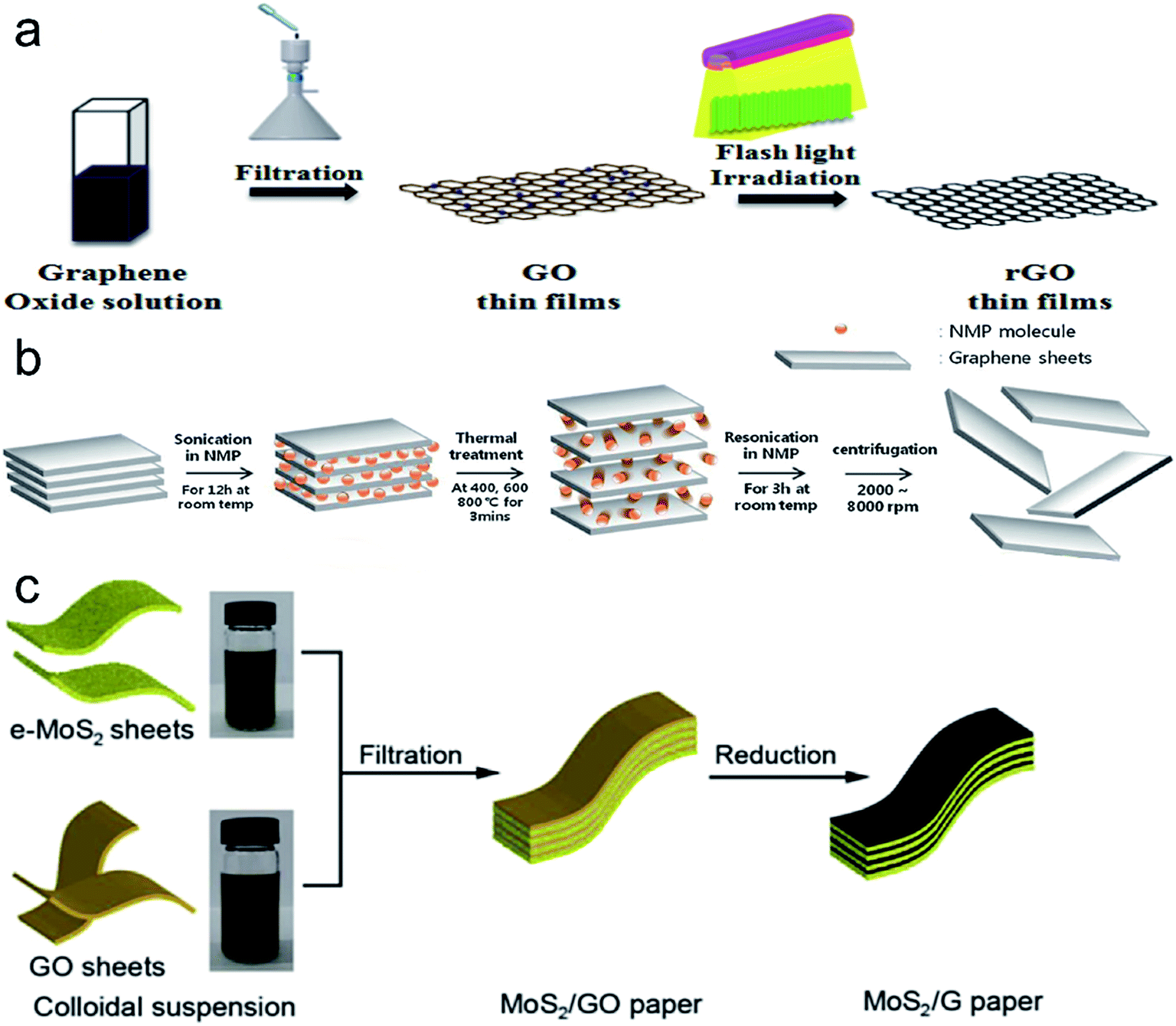 | ||
| Fig. 6 (a) Schematic diagram of the flash light irradiation process for the reduction of GO thin films (ref. 59). (b) Schematic diagram of the oxide-free graphene suspension preparation process (ref. 58). (c) Schematic layout of the preparation of MoS2/graphene composite paper (ref. 60). | ||
Graphene films or composite materials prepared by vacuum filtration method can be used as electrode material, such as, anode for lithium-ion batteries,60,68 self-powered electronics62 and field emission material.63 Yang et al. fabricated a MoS2/graphene composite film that can be used as an anode for lithium-ion batteries (Fig. 6c).60 The capacity retention of the electrode was 65.8% at a high current rate of 1000 mA g−1 and 91.1% after 100 cycles respectively. Du et al. fabricated graphene-based supercapacitors with specific capacitance of 245 F g−1 and good cycling stability of 10000 cycles. They got self-powered electronics which can be used to store solar energy by integration of graphene-based supercapacitors with high performance perovskite hybrid solar cells.62 Hybrid films of CNTs and graphene have excellent mechanical and electrical properties. These films may replace CNT films or ITO and they can be used as electrodes for supercapacitors, lithium-ion batteries and solar cells.64,66 To sum up, graphene films or composite materials fabricated by vacuum filtration method have excellent electrical performance.
The vacuum filtration method can be carried out at room temperature, and the equipment is simple and easy to operate. The thickness of graphene films can be tuned by changing the concentration and filtration volume of GO suspension, but the resulting films are generally inhomogeneous. It is difficult to achieve complete transfer of LAG films on filter membrane, and small area graphene films can be transferred relatively intact, but not uniform. There is still much work need to be done in order to get high-quality LAG films by vacuum filtration method.
2.1.5.1. Liquid–air interfacial assembly. For the interfacial assembly of GO, liquid–air interface is the most readily available. The ambient atmosphere and GO suspension are usually the gas phase and the liquid phase, respectively. Amphiphilic nature and surface chemistry activity are key factors for the assembly of GO sheets at liquid–air interface.69 Due to the amphiphilicity, GO sheets tend to move toward the interface and the movement of GO sheets can reduce the surface tension of the liquid phase, thus, it can achieve self-assembly of GO sheets at liquid–air interface.
Zhao et al. invented a modified chemical exfoliation technique to fabricate large area GO sheets.97 The maximum area of the GO sheets obtained was ∼40000 μm2. Thin GO films were prepared by self-assembly on a liquid/air interface, and then reduced by HI acid for the application of transparent conductive film (Fig. 7a). They found that the sheet resistance and transmittance of RGO films composed of GO sheets in area of ∼7000 μm2 was 840 Ω sq−1 and 78%, respectively. Evaporation-induced self-assembly of GO sheets at a liquid/air interface on glass substrate was reported by Niu et al. in 2012 (Fig. 7b), and they adopted low temperature thermal reduction at 200 °C.94 They obtained centimeter scale RGO films which exhibited high elastic modulus of 76.18 GPa and hardness of 6.89 GPa. Liquid–air interface assembly method can be applied to both flexible and non-flexible substrates and can be used to prepare hybrid films.96,98 Shao et al. presented the first example of GO/CNTs hybrid membrane which is uniform and flexible (Fig. 7c).96 In the experiment, SWCNT were dispersed into GO to form homogeneous suspension, and GO sheets serve as the surfactants owing to the amphiphilic.
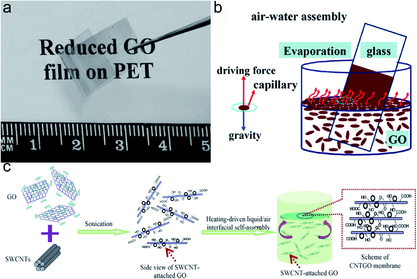 | ||
| Fig. 7 (a) A photograph of RGO film on PET reduced by HI acid (ref. 97). (b) Schematic diagram of GO film self-assembly at liquid–air interface on glass substrate (ref. 94). (c) Schematic diagram of the self-assembly of a GO/CNT hybrid membrane at the liquid/air interface (ref. 96). | ||
Langmuir–Blodgett (LB) assembly is a classical liquid–air interfacial assembly technique to prepare thin films.105–113 In a typical LB assembly process for the preparing of GO thin films, GO sheets are firstly dissolved in a volatile organic solvent and then dropped onto water surface by using a glass syringe.69,113 In general, methanol will be chosen as the volatile solvent, because it disperses GO well and can spread on a water surface rapidly. The optimum ratio of water/methanol mixture is 1:5 in most experiment. After evaporation of the volatile solvent, a monolayer film of GO sheets will form at water–air interface. Finally, the film can be transferred to a target substrate by vertical dip-coating. Fig. 8 shows a general flowchart for the synthesis of graphene films. There are mainly two interaction ways for GO sheets: edge-to-edge and face-to-face.113 Strong edge-to-edge electrostatic repulsion makes GO sheets stable and can also prevent the single layers from overlapping, while face-to-face interaction will lead to irreversible stacking. Thus, people can obtain multilayer films through layer-by-layer deposition. The morphology of GO films prepared by LB assembly can be precisely adjusted by changing the surface pressure and pH value of GO suspension.69,71,113,114 With the increase of surface pressure, GO sheets begin to fold at the contact points along edges so as to balance the pressure, leaving the interior flat and free of wrinkling.113 Further increasing the surface pressure, edge-overlapping can be firstly observed, then, the interior of GO films will wrinkle when there is no free space left at the edges of films. Hydrophilic edge groups (carboxyl, hydroxyl) and hydrophobic basal plane of GO sheet lead to its amphiphilic, pH can affect the degree of ionization of the edge carboxyl groups, so that amphiphilicity of GO can be tuned by pH.71,114 The pH value of GO suspension is often modified by adding HCl or NaOH solution. GO sheets become more hydrophilic with the increase of pH which promotes the deprotonation of the carboxyl groups. After adding HCl to neutralize the base, the surface pressure can be largely recovered but it is still smaller than the initial value, which is considered that there is a loss of material at the interface under basic conditions. Under acidic conditions, parallel wrinkles can be seen in the film.
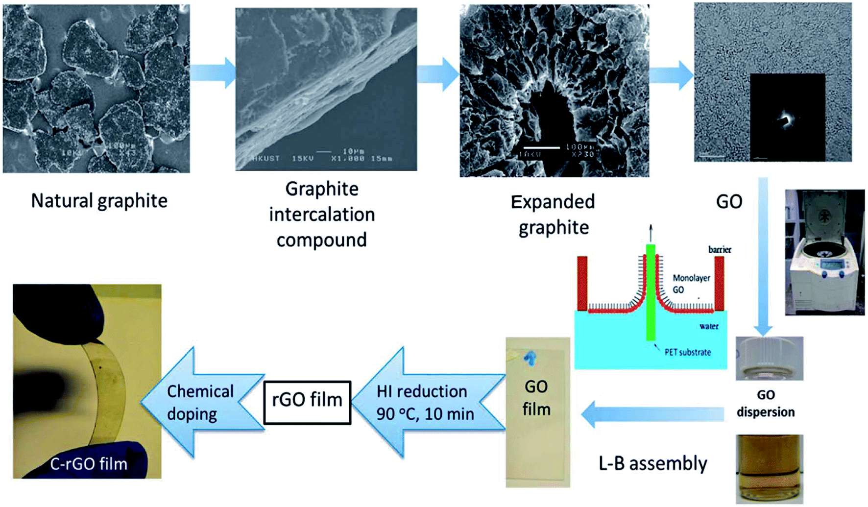 | ||
| Fig. 8 Flow chart for the synthesis of graphene thin films by LB assembly technique (ref. 106). | ||
In 2008, Li et al. reported a method to fabricate high-quality graphene sheets from graphite. About 90% of these graphene sheets were monolayer and the average size was 250 nm.111 For the first time, high-quality graphene sheets were assembled by LB technique through layer-by-layer deposition. The sheet resistance and transmittance of three-layer films on quartz were 8 kΩ and 83%, respectively. GO films prepared by LB assembly can be used as conductive electrodes.105–108,110 Lin et al. prepared transparent conductive films (TCFs) composed of ultra-large GO sheets by LB assembly followed by HI acid reduction and chemical doping treatment.106 The sheet resistance of the film was 1100 Ω sq−1 with a transmittance of 91%. In 2011, Zheng et al. produced films from ultra-large GO sheets with the sheet resistance of ∼500 Ω sq−1 with 90% transparency after thermal reduction and chemical doping treatments.108 Then, in 2012, the sheet resistance and transmittance of TCFs prepared by Zheng et al. were 605 Ω sq−1 and 86%, respectively.107 In the experiment, they adopted a chemical method to produce ultra-large GO sheets with a diameter up to about 100 μm. Both the production of large size GO sheets with high quality and the promotion of electrical conductivity are key factors for the successful preparation of TCFs with excellent electrical properties. Films composed of GO sheets can be used as two-dimensional filler for polymer nanocomposites.109 Kulkarni et al. used monolayer GO flakes as filler for polyelectrolyte, a significant increase in the elastic modulus of this composite film can be observed from 1.5 GPa of pure polyelectrolyte to about 20 GPa for only 8.0 vol% graphene oxide encapsulated membranes.
In conclusion, liquid–air interfacial assembly of GO sheets can be easily realized by using the ambient atmosphere as gas phase and GO suspension as the liquid phase. LB assembly is a classical liquid–air interface assembly technique. It is known to be the only technique that can realize layer-by-layer deposition of GO sheets and can precisely control the thickness of the film by repeated deposition.105,107 Graphene films fabricated by LB assembly can be transferred to various substrates and it is amenable for large-scale production and industrial applications.
2.1.5.2. Liquid–liquid interfacial assembly. Liquid–liquid interface is another ideal 2D platform for the assembly of GO sheets to form films.69,71 The self-assembly interface is usually formed between a hydrophobic organic solvent and GO suspension. The driving force for the self-assembly of GO sheets at the liquid–liquid interface is the minimization of interfacial free energy.102 After the formation of GO membrane at the interface, it can be transferred to target substrate by lift-up technique.
In 2008, Biswas et al. investigated the formation of closely packed monolayer of highly hydrophobic graphene nanosheets at a liquid–liquid interface.102 They chose chloroform as organic solvent to disperse graphene nanosheets, then, two distinct phases formed after adding water to the mixture. A large interfacial area between the two phases can be created through sonication. Graphene nanosheets preferred to be adsorbed at the interface and to form a large area closely packed monolayer driven by the minimization of interfacial free energy. These graphene films exhibit good properties. The average conductivity of 4 nm thick graphene films is more than 1000 S cm−1 and the transmittance is more than 70% at a wavelength of 550 nm. Chen et al. thought that organic solvent evaporation provides little driving force which results in slow transport of GO sheets to the interface.100
In 2011, Chen et al. reported an ethanol-assisted self-assembly method which allowed fast preparation of GO-based film at pentane–water interface (Fig. 9a). They studied the effect of ethanol and found that it served as a nonsolvent for GO suspension. Due to the less dispensability of GO in ethanol, the stability of GO suspension is compromised when ethanol is injected into it. Then, GO sheets are pushed to the pentane–water interface and aggregate to form a film. This approach accelerates the liquid–liquid interfacial assembly and opens up opportunities to fabricate new GO-based hybrid films. The transmittance of resulting RGO films can be tuned from 72% to 97% at 550 nm by changing the concentration of GO suspension. The surface resistivity varied from 8.3 to 464.6 kΩ sq−1. In 2015, Arapov et al. adopted oil–water interfacial assembly to prepare LAG thin films.103 Firstly, they fabricated expanded graphite via graphite intercalation method followed by thermal expansion. In the experiment, both donor and acceptor-type graphite intercalation compounds were investigated. The resulting material was dispersed in a mixture of isopropanol and propylene glycol with the optimum volume ratio of 3:2. Finally, graphene thin films were self-assembled at the oil–water interface by adding graphene suspension to the interface. Those films were transferred to target substrate by lift-up technique (Fig. 9b). The area of the graphene films were more than 50 cm2 and potentially more than 1 m2. The sheet resistance and transmittance of those films after thermal annealing varied from 10 to 0.8 kΩ sq−1 and 75–45%, respectively.
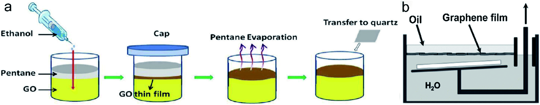 | ||
| Fig. 9 (a) Schematic illustration of ethanol-assisted formation of GO thin film at pentane–water interface (ref. 100). (b) Schematic diagram of lift-up transfer technique (ref. 103). | ||
2.1.5.3. Liquid–solid interfacial assembly. The driving force for liquid–solid interfacial assembly is related to the amphiphilic nature and the chemical activity of GO sheets.69 There are many types of interactions between GO sheets and solid surface, including covalent bonding, hydrogen bonding, π–π interaction, electrostatic effects and potential chemical reaction. For the first time, Liu et al. obtained paper-like GO films by self-assembly of GO sheets on the surface of aluminum foil.104 In the experiment, GO aqueous suspension was casted on the aluminum foil followed by drying at 40–60 °C at ambient pressure, and after that a black GO/Al thin film was formed. The formation of paper-like GO thin films are affected by many factors, such as the evaporation, upward gas flow, and the increasing hydrophobicity of GO reduced by Al foil. The structure of GO films can be controlled by adjusting the concentration of GO. The thickness and the area of the film can be controlled by changing the usage amount and concentration of GO suspension.
In summary, the self-assembly of GO sheets at various interfaces is a self-concentration process. The interfacial assembly method has many advantages. It is an effectively method in controlling the homogeneity of film thickness and the layers through layer-by-layer deposition. The films of different sizes can be obtained by changing the size of the interfaces. The resulting films can be easily transferred to various substrates by lift-up technique or dip-coating method. Besides, it is possible to fabricate composite films by dispersing bi- or multi-components in GO suspension. But, there are also many challenges. (1) A deeper understanding of interfacial assembly and the precise control of self-assembly of GO sheets at various interfaces remain to further investigation. (2) It is still very difficult to precisely control the microstructure of self-assembly of GO sheets in its large scale preparation and real applications. (3) More attention should be paid to low cost and to improve scalable assembly techniques as well as effective and nondestructive reduction techniques.
 | ||
| Fig. 10 (a) Schematic diagram of electrostatic spray deposition (ref. 75). (b) A CCG film on 4-inch quartz wafer (ref. 77). (c) Photograph of a 9 × 6 cm2 graphene paper (ref. 73). | ||
In 2007, Gilje et al. employed spray coating method to prepare graphene films.76 A GO aqueous dispersion was deposited onto preheated SiO2 substrates followed by chemical reduction using hydrazine. GO sheets can be deposited onto various substrates of any size by this method and highly uniform graphene sheets can be obtained with any desired coverage density. In 2010, for the first time, Pham et al. employed spray deposition of GO–hydrazine dispersion (a mixture of GO and excessive hydrazine monohydrate) to prepare chemically-converted graphene (CCG) films.77 The preparation of thin films and reduction of GO to CCG were carried out simultaneously after depositing the mixture on preheated substrate. They successfully prepared a 4-inch, uniform CCG film on quartz wafer (Fig. 10b). The successful preparation of a stable graphene aqueous solution and RGO dispersion are critical for both basic research and practical applications of graphene. In 2011, Pu et al. studied the dispersion of graphene in aqueous solution with different types of surfactants including cationic, anionic, non-ionic and polymer types.78 Finally, they found that the best graphene dispersion was prepared by non-ion type surfactant—polyoxyethylene-nonylphenylether at a concentration of 200–300 ppm. The graphene suspension can be spray-coated onto various substrates to form films.
In 2012, Min et al. reported a facile way to fabricate stable RGO dispersions in aqueous or organic media by adjusting the degree of reduction and pH of RGO dispersion.72 The degree of reduction determined the surface properties and pH affected the surface potential of the dispersion. Uniform and transparent conductive RGO films can be obtained by spray coating of well dispersed RGO aqueous solution on various substrates. In 2014, Xin et al. adopted electrostatic spray deposition integrated with R2R process to prepare LAG papers.73 The graphene paper was deposited on Al foil and was peeled off from the substrate by immersing into water. This is attributed to their differences in surface properties and wettability. They got a 9 × 6 cm2 graphene paper (Fig. 10c), an 18 inch graphene paper strip and a graphene paper roll with width of 4.5 inch, respectively.
In summary, all of these solution processing methods mentioned above can be easily realized on various substrates at low temperature. But the graphene films often suffer from poor quality, for instance, agglomeration of nanosheets and nonuniformity of the film. RGO films have an important feature of low cost due to the ample supply and low price of graphite. Besides, it is easy to achieve mass production of LAG films by these methods. Furthermore, reduction methods, mainly including thermal reduction and chemical reduction, have a great impact on the quality of RGO thin films.59
Both thermal reduction and chemical reduction have drawbacks. Thermal reduction is generally operated at high temperature in inert gas or vacuum environment which is incompatible with most device fabrication techniques, especially unsuitable for heat-sensitive substrates such as PET. Chemical reduction often takes a long time and needs to use toxic hydrazine. Recently, Park et al. reported a new reduction method—exposure GO films to flash light irradiation which can be performed in room-temperature ambient conditions and only needs a few milliseconds. There are many reactive sites in GO films including hydroxyl, carboxyl and epoxy groups which can be used for chemical functionalization, but these groups will reduce the conductivity and increase interlayer spacing of films. After reduction treatment, the content of these groups can be reduced and the conductivity of RGO films can also be improved. Among all these methods, rod-coating may be the most effective method which can get 20 × 47 cm2 GO film, and it can also precisely control the thickness of GO films from a single layer to tens of layers by adjusting the concentration of the GO solution or the diameter of the rod wire.
2.2. CVD method
At present, CVD is the most popular and most practical method to synthesize LAG films. The growth mechanism of CVD is self-limiting.115–117 For CVD method, large area and high quality graphene films are produced by the catalytic decomposition of hydrocarbons on a metal (for example, Cu, Ni, Pt) surface which has catalytic activity at high temperatures. Then the films can be transferred to a target substrate by etching away the metal substrate or by R2R transfer techniques. In this review, we mainly discussed two CVD methods: thermal CVD27,32,37,39 and microwave plasma-enhanced (MWP) CVD.36,118–135The first report on CVD synthesis of graphene films was published in 2006.27 Somani et al. chose camphor as the starting material which is natural, environmental friendly and low-cost. They employed thermal CVD method to synthesize PFLG films from camphor pyrolysis on Ni substrate. In this experiment, camphor was firstly evaporated at 180 °C and then pyrolyzed at 700–850 °C with argon as carrier gas. This method did not require vacuum system and the reaction temperature was also relatively low. Finally, they got PFLG films with graphitic structure down to about 20 graphene layers. Since then, CVD has developed by many researchers to a scalable and reliable method for the preparation of LAG. Thermal CVD is often performed on metal substrates, among which Cu and Ni substrates are most commonly used ones.30,136
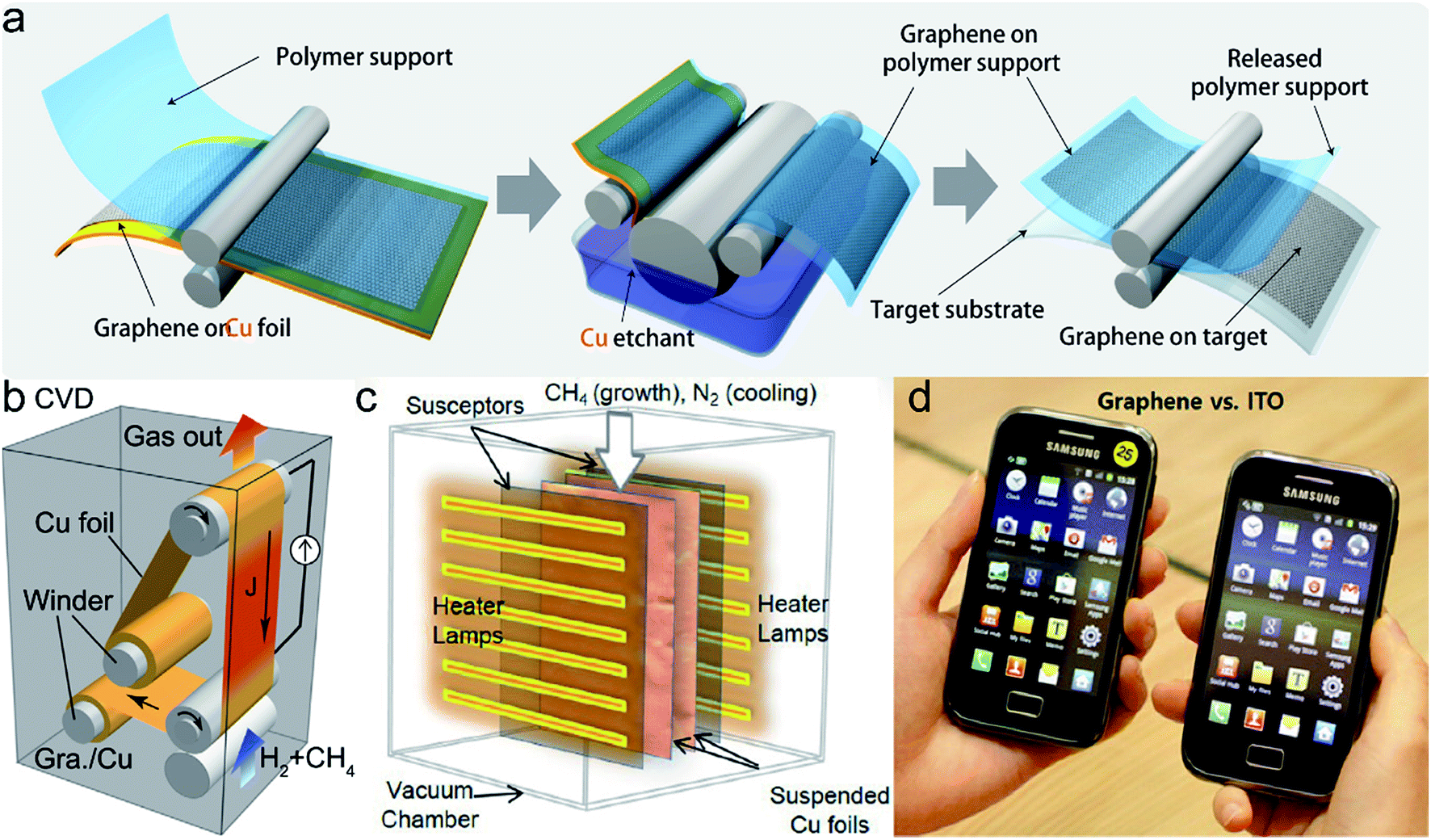
In 2009, there was a seminal breakthrough as researchers discovered that the growth of graphene on copper was self-limited to a single layer.30 Since then, the development of CVD method has been very fast. In 2010, Bae et al. successfully prepared 30-inch graphene films by combining CVD method and R2R transfer method (Fig. 11a).32 The sheet resistance of films was as low as ∼125 Ω sq−1 with 97.4% transmittance, and the films exhibited half-integer quantum Hall effect. In the CVD process, firstly, Cu substrate was heated to 1000 °C followed by annealing for 30 min in order to produce high-quality graphene films. Then, in order to achieve film growth, gas mixture of CH4 and H2 was flowed with rates of 24 and 8 sccm respectively at 460 mTorr for 30 min. Finally, the sample was cooled to room temperature. In R2R process, thermal release tap was firstly adhered to the resulting graphene film on Cu substrate by applying pressure between two rollers. Then, Cu substrate was etched away by immersing it into Cu etchant. The tap/graphene film was rinsed with deionized water to remove residual etchant. Finally, the tap/graphene film and a target substrate were inserted between the rollers simultaneously. The graphene film was transferred to target substrate by heating the rollers at 90–120 °C.
 | ||
| Fig. 11 (a) Schematic diagram of the roll-to-roll production of graphene film (ref. 32). (b) Schematic diagram of R2R CVD system using selective Joule heating (ref. 37). (c) Schematic illustration of RT-CVD synthesis setup (ref. 39). (d) Photograph of the touch screen fabricated by graphene film (left) and ITO (right) installed in a mobile phone, respectively (ref. 39). | ||
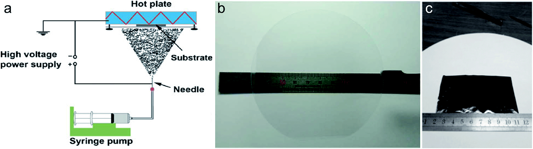
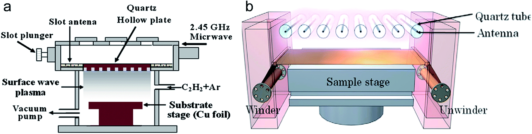
In 2013, Sony Corporation successfully prepared a 100 m-long, 230 mm-wide graphene film by employing R2R CVD method (Fig. 11b).37 The sheet resistance of graphene films was about 500 Ω sq−1 before doping and 200 Ω sq−1 after doping with AuCl3. It was a big breakthrough for the preparation of LAG films and brought new hope to researchers and enterprisers. They used selective Joule heating of the Cu foil to achieve R2R production of high quality graphene. The Cu foil was wound on the R2R system for 100 m and it can be heated to 1000 °C owing to small emissivity and heat conduction. The first 52 m graphene film was grown at 950 °C by applying a constant direct current J = 82 A mm−2, the remaining 48 m graphene film was grown at 980 °C (J = 83 A mm−2). Ryu et al. adopted hydrogen-free rapid thermal CVD (RT-CVD) method (Fig. 11c) combined with R2R transfer technique to produce homogeneous graphene films.39 Cu foil was mounted vertically in the heating system composed of 24 halogen lamps which can radiate light ranging from visible to infrared wavelengths. A graphite susceptor which can efficiently transform near-infrared light to thermal radiation was adopted because visible wavelength was mostly reflected by the Cu surface. Sufficient energy can be obtained by this method, so that the Cu foil can be heated to about 1000 °C. In the experiment, the optimum temperature was ∼970 °C, CH4 was used as carbon source and N2 was used to cool the foils. It only took 40 min throughout the experiment without using hydrogen. The sheet resistance of graphene/PET film was 249 ± 17 Ω sq−1 which indicates excellent electrical performance. They successfully fabricated a capacitive multitouch device which was installed in a mobile phone (Fig. 11d) by using the graphene film.
In the initial stage, few-layer graphene118,120 or graphene sheets119 can be prepared by using MWP CVD method. Malesevic et al. reported the synthesis of few layer graphene by MWP CVD method in 2008 and further investigated the growth mechanism in 2009.118,120 Those graphene flakes composed of 4–6 atomic layers were deposited at 700 °C on various substrates. They reported that few-layer graphene was aligned vertically to the surface of substrates and proposed a three-step growth mechanism. In 2015, Park et al. also employed microwave plasma method to prepare vertically standing multi-layer graphene films on various substrates at a temperature ranging from 432 to 225 °C and investigated the growth mechanism.134 In 2011, Kim et al. adopted MWP CVD method to prepare centimeter scale monolayer graphene on nickel foil at temperatures ranging from 450 to 750 °C.121
Kalita et al. has made great contributions in the preparation of graphene films by using surface wave plasma CVD method.122–124 They employed microwave assisted surface wave plasma CVD (MW-SWP-CVD) method (Fig. 12a) to prepare graphene films on Cu foil at a temperature as low as 240 °C.122 The resulting films were continuous and uniform, but there still existed defects. The lowest sheet resistance of the graphene film was 10.03 kΩ sq−1 with 73% transmittance at 550 nm. They thought that this technique can be scaled up for metre-scale deposition of graphene films. Then, in 2012, they used camphor as a solid carbon source to prepare graphene films below 600 °C.124 They found that camphor molecules could decompose effectively under the influence of the plasma by dehydrogenation, and then carbon radicals segregated on substrate surface to form film. They fabricated a transparent electrode by transferring graphene film on plastic substrate. The sheet resistance and transmittance of the electrode was 8.23 kΩ sq−1 and 85.4% at 550 nm, respectively. Polydimethylsiloxane can also be used as a solid carbon source to prepare graphene films.125 Hiramatsu et al. thought that excess ion bombardment generated by the plasma would damage the deposits on substrates, so they invented a new method which can simply control the position of the plasma ball and reduce ion bombardment on the surface of substrates by installing a grounded molybdenum mesh over the substrate plate.126
 | ||
| Fig. 12 (a) Schematic diagram of the MW-SWP-CVD system used for the preparation of graphene films at low temperature (ref. 122). (b) Schematic of R2R CVD apparatus for graphene film deposition (ref. 36). | ||
Yamada et al. has also made many contributions in the preparation of LAG films.36,129–133,135 In February 2012, they invented a R2R MWP CVD apparatus (Fig. 12b) equipped with a pair of R2R winder and unwinder system.36 The deposition area was 294 × 480 mm2. They successfully prepared few-layer graphene films in width of 294 mm on Cu copper bellow 400 °C. A few months later, they successfully prepared graphene films on Al and Cu substrates at around 300 °C by surface wave plasma CVD (SWP CVD) method.129 In 2013, they used poly(methyl methacrylate) as solid carbon source to prepare graphene films on Cu surface at 280 °C.135 They obtained graphene films which were consisted of single- or double-layer graphene flakes. The average optical transmittance was about 96% between 400 and 800 nm and the sheet resistances were ranging from 600 to 5000 Ω sq−1. Both electrical properties and domain sizes of graphene films fabricated by MWP CVD were investigated.131,133 The Hall mobility was up to 100–1000 cm2 V−1 s−1 under a low carbon concentration and average domain size was around 30–100 nm. And the crystallinity of the synthesized graphene films can be improved by plasma pretreatment of substrate surface using He/H2.132
In conclusion, although we can gain LAG films by using CVD method even at lower temperatures, it is difficult to precisely control the number of layers and the quality of graphene films. Besides, the performance of graphene films will be destroyed more or less after transferring.137 There are still many challenges for large-scale production of large-area and high-quality graphene films. More detailed information can be obtained in Tables 2 and 3.
| Method | Classification | Representative work | Reference | Concentration/temperature | Merit/demerit |
|---|---|---|---|---|---|
| Chemical assembly | Rod-coating | In 2012, Wang et al. prepared a RGO film—20 × 47 cm2 | 35 | 0.05–2.5 mg mL−1 (GO suspension) | Merits: growth on various substrates; low temperature; simple fabrication procedure. Demerits: agglomerate after solvent evaporation; having functional groups after reduction; difficult to mass production |
| Spin-coating | In 2010, Yamaguchi et al. prepared a 300 mm water-scale GO film | 50 | 0.4–5 mg mL−1 | ||
| Dip-coating | In 2013, Cao et al. prepared a paper-like film—20 × 23 cm2 | 56 | 0.1–1 mg mL−1 | ||
| Vacuum-filtration | In 2008, Eda et al. prepared a GO thin film—10 cm2 | 29 | — | ||
| Interfacial assembly | In 2015, Arapov et al. reported that they can get films more than 50 cm2 | 103 | — | ||
| Spray-coating | In 2014, Xin et al. prepared a 18 inch graphene paper strip | 73 | — | ||
| CVD | Thermal CVD | In 2010, Samsung—30 inch in diagonal | 32 | Higher than 1000 °C | Merit: self-limiting growth; gain LAG film; large single-crystal growth; easy to transfer to arbitrary substrates. Demerit: transfer can damage the quality and performance of graphene; somewhat expensive; high growth temperature; difficult to precisely control layers |
| In 2013, Sony Corporation—100 m-long, 230 mm-wide | 37 | ||||
| MWP-CVD | In 2011, Kim et al. fabricated LAG-based films—23 × 20 cm2 | 34 | Lower than 1000 °C | ||
| In 2012, Yamada et al. prepared LAG films—294 × 480 mm2 | 36 | (200–800 °C) |
| Method | Properties of graphene film | Relative merits |
|---|---|---|
| Rod-coating | Continuous, uniform, flexible, good transparency and conductivity | Low-cost, easy to operate, scalable, precise in thickness control, applicable to various substrates |
| Spin-coating | Continuous, uniform, thin, good transparency and conductivity | Low-cost, easy to operate, thickness of film can be adjusted by changing the concentration of GO suspension and cycles of coating |
| Dip-coating | Aggregation of GO sheets, non-uniform, few layer, high surface coverage, tunable transmittance | Low-cost, easy to operate, continuous, thickness can be adjusted, large area production can be achieved through mechanization |
| Vacuum filtration | Inhomogeneous, incomplete transfer, good conductivity and mechanical properties, heterogeneity of the layer number | Simple, cheap, easy to operate, thickness can be tuned |
| Interfacial assembly | Having wrinkles, good transparency and conductivity, high elastic modulus, diverse microstructure and morphologies | Up-scalable, self-concentration process of GO sheets, films can be easily transferred to various substrates by lift-up technique, control layers by layer-by-layer deposition |
| Spray coating | Aggregation of GO sheets, non-uniform | Thickness of films can be adjusted by changing solution concentration and the time of deposition |
| CVD | Large area, high surface coverage, high quality, excellent optical and electrical performance | Self-limiting growth, large-scale industrial production, gain LAG film, large single-crystal growth, easy to transfer to arbitrary substrates |
3. Applications in membrane separation
Pristine graphene without any defects is impermeable to molecules as small as hydrogen and helium, because the electron density of its aromatic rings is enough to repel atoms to pass through this membrane. However, graphene films with nanopores can be used as molecular separation membrane.138 Due to its negligible thickness, chemical stability and high mechanical strength, graphene has become an ideal membrane material that can be used for molecular separation. In this review, we mainly discuss applications of graphene films in water desalination,139–161 DNA sequencing162–182 and gas separation.183–2023.1. Desalination and power generation
With the increase of population and factories as well as increased water pollution, freshwater resources are becoming increasingly less and desalination is expected to be an important way to get clean water. In recent years, both reverse osmosis (RO) and forward osmosis (FO) technologies have attracted growing attention in desalination. The improvements of the water flux, salt rejection, mechanical strength and anti-pollution of the membranes are critical to the two osmosis technologies. A lot of simulation142,152–155,158–161 and experimental researches.140,141,143,144,147,150,151,156 indicated that large area, porous graphene films exhibited high water flux and salt rejection for desalination even under low pressure conditions. Gai et al. reported a FO system using fluorinated porous graphene as the FO membrane which has an excellent performance for salt rejection, especially the water flux is about 1.8 × 10⁴ times higher than that of a typical cellulose triacetate membrane.142 Besides, due to the superior strength (1 TPa) and thickness (one carbon diameter), nanoporous graphene is a potential semi-permeable membrane where a fabric support layer is not necessary.For the first time, Sint et al. studied ion selective permeability through functionalized graphene nanopores, they found that negatively charged graphene nanopores allowed passage of cations, and vice versa.158 Experimental results showed that graphene films with nanopore can serve as ionic sieves of high selectivity. In 2010, Suk et al. investigated the transportation of water through a porous graphene film, and compared it with CNT membrane.155 The pore diameter is critical to whether the graphene film can achieve a higher transport flux than CNT membrane. They found that graphene film can be used as a highly efficient water transporter when the pore diameter is larger than 0.8 nm.
Cohen-Tanugi et al. has done a lot of work in this area.152,154,160,161 In 2010, they investigated the effect of pore size, chemical functionalization and applied pressure on film performance.152 They found that the maximum pore diameter was around 5.5 Å. Hydrophilic functional groups at the edge of the pore could increase the water flux, but the rejection performance was destroyed as the pressure increases. The water permeability is ranging from 39 to 66 L cm−2 d−1 MPa−1 (with 100% salt rejection) which is 2 orders of magnitude higher than that of the general RO membranes. They also investigated the water permeability of nanoporous graphene at external pressure employed in RO desalination.154 Ultrahigh water flux of 1041 ± 20 L m−2 h−1 bar−1 was got at a pressure of less than 100 bars. The mechanical strength of nanoporous graphene was also studied.160 Both the size and spacing of graphene nanopores and the radius of the pores in support layer can affect the maximum pressure that nanoporous graphene film can withstand. When pores in supporting layer are smaller than 1 μm, nanoporous graphene film can withstand hydraulic pressures of 57 MPa which is nearly 10 times higher than typical RO membrane.
Konatham et al. investigated the effect of pore size in pristine graphene and functionalization of pores on the performance of the membrane in 2013.159 Results showed that graphene with pristine pores in size of 7.5 Å can be used in water desalination effectively and the functionalized pores can generate large free-energy barriers for salt ions due to electrostatic and steric effects. Nicolaï et al. found that water permeability in graphene oxide framework membranes can be tuned from 5 to 400 L cm−2 d−1 MPa−1.153
Many experimental studies on LAG membrane were carried out and results showed that LAG membrane has excellent desalination performance which is consistent with the simulation results.140,141,143,144,147,150,151,156 In 2013, Hu et al. adopted layer-by-layer deposition of GO nanosheets to prepare GO membrane which was cross-linked by 1,3,5-benzenetricarbonyl trichloride on a polydopamine-coated polysulfone support (Fig. 13a).140 After coating with 5–50 layers of GO, water flux of the composite membrane ranges from 80 to 276 L m−2 h−1 MPa−1 which is 4–10 times higher than that of most commercial nanofiltration membranes. The rejection of monovalent and divalent salts was only 6–46%, but the rejection rates of Methylene blue and Rhodamine-WT were 46–66% and 93–95%, respectively. Choi et al. found that GO sheets on polyamide membrane can improve the durability of the RO membrane.141 The GO layer can resist degradation of polyamide membrane induced by fouling and chlorination, but will not reduce the water flux.
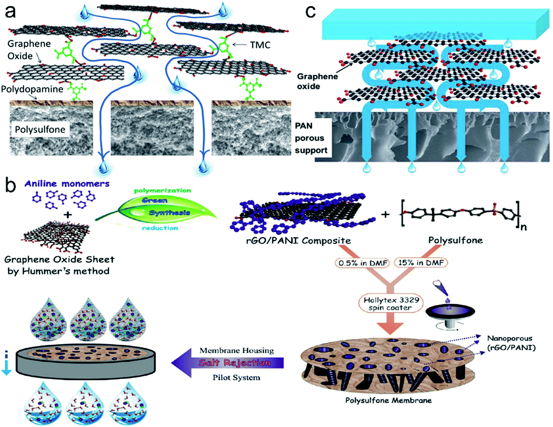 | ||
| Fig. 13 (a) Schematic illustration of water transportation through GO/polysulfone composite membrane (ref. 140). (b) Schematic diagram for the preparation of the PSf-rGO/PANI composite membrane (ref. 156). (c) Schematic representation of the mechanism for water molecule transport through GO/PAN composite membrane (ref. 144). | ||
In 2014, Akin et al. prepared a polysulfone-reduced graphene oxide/polyaniline (PSf-rGO/PANI) composite material (Fig. 13b) which was used as desalination membrane.156 The rGO/PANI composite material was first produced by an enzymatic-reaction-based approach, and then it was dispersed in PSf. After phase inversion polymerization, PSf-rGO/PANI composite membrane was got finally. The maximum salt rejection of the membrane with 0.5% (w/w) rGO/PANI loading is 82% for NaCl at 10 bar pressure, and water flux ranges from 30 to 180 L m−2 h−1 at pressure of 4–20 bars. Fluorine-terminated graphene membrane can also be used to remove copper and mercury from aqueous solution.143 In 2015, Liang et al. prepared a GO/polyacrylonitrile (GO/PAN) composite membrane (Fig. 13c) as pervaporation membrane for desalination.144 The water flux is up to 65.1 L m−2 h−1 with 99.8% of salt rejection at 90 °C. There are nanometer-sized intrinsic defects on graphene film prepared by CVD method and large tears may form after transferring. Thus, O'Hern et al. adopted a multiscale sealing procedure to seal these defects and then used high-energy gallium ion bombardment to produce subnanometer pores in the graphene film.151 The water flux of the membrane is 1.41 ± 0.23 L m−2 h−1 bar−1 and rejection of MgSO4, allura red and dextran are ∼70%, ∼90% and ∼83%, respectively.
Surwade et al. employed oxygen plasma etching process to create nanometer-sized pores in monolayer graphene film and investigated water desalination performance of the nanoporous film.150 The salt rejection is nearly 100% and the water flux is up to 106 g m−2 s−1 at 40 °C under the condition of pressure difference as a driving force. It is 5 orders of magnitude higher than water flux (70 g m−2 s−1 atm−1) measured using osmotic pressure as driving force. He et al. prepared a GO/polyamide composite membrane for water desalination and investigated antibacterial activity of the membrane.147 Water flux of the composite membrane with 0.12 wt% of GO increased to 0.219 L μm m−2 h−1 bar−1 and salt rejection is nearly 90% at 20 bar. The membrane exhibits a strong antibacterial activity, thus it can be used for the purification of biologically active waste slurries. Studies show that nanoporous graphene film is an ideal material for water desalination.139,145,146,148,149,157 The thickness of graphene film is only one atomic layer and the surface is smooth and frictionless, so high water permeability and low energy consumption can be achieved. The durability of the composite desalination membrane can also be improved due to high mechanical strength and chemical inertness of graphene.
In fact, there are many difficulties in applying LAG films to desalination field. For example, the cost of graphene film is still very high; water flux of the membrane is limited by the concentration polarization phenomenon, fouling effects and inherent thermodynamic limit of the separation process; precisely controlling the pore sizes and the distribution and creating nanopores in LAG film are difficult; reducing energy consumption and infrastructure costs of existing desalination technologies remains a challenge. Although the development of LAG film in seawater desalination is still immature now, but it has great potential application in the field of desalination and may lead the development of the next generation water treatment membrane.
To date, FO has been one of the most promising approaches for power generation from the mixing of fresh water and seawater in estuaries.203–207 However, existing FO membranes suffer from low power densities, which seriously hinder its practical applications in power generation. The enhancement of the water flux of a FO membrane is therefore greatly beneficial for power density.208 Internal concentration polarization (ICP) caused by bulky support layers of membranes has been one of the most common and unavoidable phenomena in osmotically driven membrane processes, which is the most important factor in reducing the water flux. Fortunately, porous graphene with its incomparable strength can be used as a FO membrane without the requirement of a support layer, and consequently, exhibits zero ICP. Gai et al. first reported that the water flux of fluorinated porous graphene membrane is about 1.8 × 10⁴ times higher than that of a typical cellulose triacetate membrane.142 Such high water flux will certainly bring about a very high power density in pressure retarded osmosis power generation. This work may generate potential opportunities for functionalized graphene in FO power generation.
3.2. DNA sequencing
Graphene film with single-atom-thick has excellent mechanical strength and electrical sensitivity which makes it an ideal material for high-resolution, nanopore-based molecule detectors compared with traditional solid-state nanopores made from silicon nitride, aluminum oxide or silicon oxide. Recent researches have found that nanoporous graphene membranes can be used for DNA sequencing. The experimental operation of DNA sequencing is summarized as follows. Firstly, nanometer-scale pores are formed in graphene films using electron beam. Then, the membrane system composed of graphene film, silicon nitride, silicon and other components is placed in a measurement cell which is separated into two compartments and each compartment is filled with ionic solutions electrically contacted with electrodes. Finally, DNA molecules are added into a compartment and a bias voltage is applied to the other compartment, which will cause changes in the current when DNA molecule translocates through the nanopore. A typical graphene nanopore device for DNA sequencing is shown in Fig. 14a.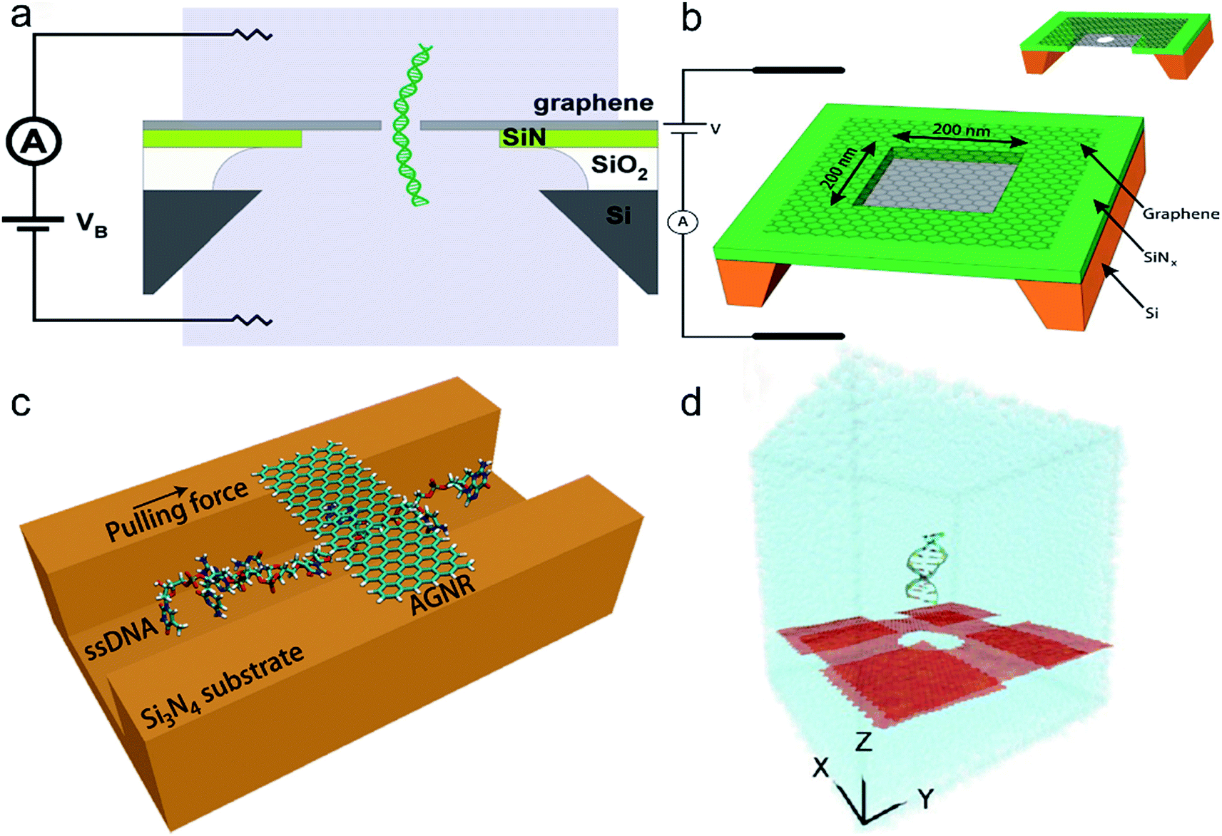 | ||
| Fig. 14 (a) A typical graphene nanopore device for DNA sequencing (ref. 164). (b) A graphene membrane with nanopore used as trans-electrode membrane (ionic solutions are not shown) (ref. 163). (c) Schematic of a nanochannel device functionalized by a graphene nanoribbon for DNA sequencing (ref. 177). (d) Schematic diagram of a graphene nanopore with four additional graphene sheets in order to retard the translocation of DNA (ref. 171). | ||
It has been nearly 40 years since the first DNA sequencing by Sanger technique.209,210 Sanger sequencing is considered to be the first-generation DNA sequencing technique. After 30 years of development, it can achieve read-lengths of up to ∼1000 base pairs (bp) and per-base ‘raw’ accuracies as high as 99.999%.170,181 The initial draft of the first human genome sequence spent about $300 million and the second genome sequence of nonhuman primate (the rhesus macaque) cost $22 million.173 The demand for reducing the cost stimulated the development of second-generation sequencing methods including microelectrophoretic methods, sequencing by hybridization, real-time observation of single molecules and cyclic-array sequencing, etc.170,181 In order to reduce the cost of genome sequencing to $1000, researchers are trying to find more efficient sequencing technology. Third-generation sequencing methods will take advantage of the characteristic electrical conductance of the four different nucleotides.178
Due to one-atom thickness and excellent electrical sensitivity, graphene has aroused the interest of researchers in nanopore sequencing. At the beginning, the electronic properties of DNA bases have been investigated by researchers.168,169 Zwolak et al. investigated charge transport in single-stranded DNA in the direction perpendicular to the backbone axis in 2005.168 They found that each nucleotide carried a different electrical signature which was independent of the nearest-neighbor nucleotides, and the electric currents of different nucleotides were adenine > guanine ∼ cytosine > thymine (A > G ∼ C > T). Xu et al. also found that different DNA bases showed base-specific electronic signatures.169 This makes it possible for electronic sequencing of DNA by exploiting different electrical signals of four nucleotides.
There have been many literatures related with DNA sequencing using porous graphene films since 2010.163–167,171,172,174–180 Postma chose graphene nanogaps as the electrode as well as the membrane material for rapid sequencing of a single DNA molecule.175 The translocation speed can be affected by pore size, aspect ratio, DNA–pore interaction strength and the unfolding speed of DNA into the pore. For the first time, Merchant et al. experimentally realized the translocation of DNA through graphene nanopores in diameter of 5 to 10 nm.164 The blocked currents of DNA translocation through graphene nanopores were higher than that through traditional solid-state nanopores, but ion current noise levels were higher than that of SiN nanopores. They found that current noise can be reduced by coating the graphene film with thin titanium dioxide layer. Schneider et al. also investigated DNA translocation through graphene nanopores with diameter of 10–25 nm drilled by electron beam.165 The average translocation time is 2.7 ± 0.8 ms for the nonfolded DNA which is higher than that for SiN nanopores (1.2 ± 0.3 ms). Nelson et al. adopted density functional theory for the calculation of electrical current and conductance perpendicular to the DNA backbone resulting from translocation of single-stranded DNA through graphene nanopore.176 They found that the proposed device was able to discriminate different nucleotides due to significant differences in the conductance spectra. Garaj et al. immersed graphene membrane in an ionic solution, therefore producing a new electrochemical structure of graphene which was called trans-electrode (Fig. 14b).163 A nanometer-sized pore in the graphene trans-electrode membrane can increase its ionic conductance by orders of magnitude.
When a DNA molecule passes through the nanopore, the ionic current can be transiently reduced or blocked and changes in ion current can reflect both polymer size and conformation. Then, in 2011, Min et al. designed a novel device composed of a fluidic nanochannel functionalized with a graphene nanoribbon for fast DNA sequencing (Fig. 14c).177 The π–π interaction between graphene and nucleobases was strong to sustain the stacking structures for current measurements, but it was weak compared with external force, so as not to affect the translocation of DNA through the nanochannel. In 2012, Wells et al. assessed the applicability of graphene nanopores for DNA sequencing by simulation.167 They found that different DNA nucleotides showed different ionic current blockades which represented the nucleotide type.
In 2013, Lv et al. investigated the impact of the number of layers of a graphene nanopore on DNA translocation by molecular dynamics simulations and potential of mean force (PMF) calculations.172 They found that the translocation velocity of DNA can be slowed down by reducing the pore size and increasing the thickness of graphene, and the translocation velocity was more sensitive to the number of graphene layers when the size of the nanopores is 2.4 nm. Liang et al. also theoretically studied the translocation of DNA through multilayer graphene nanopores in 2014.179 They found that multilayer graphene nanopores within 7 layers were superior to monolayer graphene in DNA sequencing and the resolution of DNA sequencing can be improved by modifying the nanopore surface. Kumar et al. investigated the impact of substrate materials and membrane thicknesses on noise characteristics of graphene nanopore devices.174 Results showed that fewer layer graphene transferred on to SiNx/quartz substrate possess lower noise, higher blockade current and signal to noise ratio. Avdoshenko et al. designed a new DNA sequencing setup in which four additional graphene plates were deposited on top of the main graphene platform (Fig. 14d).171 This device could retard the DNA translocation and the translocation velocity was estimated to be 17 bp ns−1 for an electric potential intensity of 2 V. Graphene nanopore geometries can also affect DNA sequencing.166 Zhang et al. found that an axisymmetric nanopore was more suitable for DNA sequencing than an asymmetric nanopore. These studies in DNA sequencing will deepen people's understanding of genome and can enhance the control and treatment of diseases.
Both theoretical and experimental studies have shown that graphene membrane with nanopores is a good platform for DNA sequencing due to its one-atom thickness, high conductivity and mechanical stability. The preparation of sample is simple and cheap because it only needs a small amount of chemical substances.182 For an ideal nanopore sequencing method, both purified fluorescent reagents and amplified genomic DNA are not required, thereby eliminating enzymes, cloning and amplification steps. Graphene nanopore device has the potential for rapid and inexpensive detection of DNA. However, DNA sequencing by graphene nanopores is currently only in its infancy, there are still a lot of work needs to be done. One of the challenges is lowering the cost of whole-genome sequencing to a few hundred dollars. Reducing the current noise and improving signal-to-noise ratios of nanopore-based graphene films is the second important challenge. Thirdly, how to make graphene nanopores with particular size and shape is a critical issue for DNA sequencing which needs to be resolved as soon as possible. Last but not the least, the mechanism of nanopore sequencing and stochastic motion of the DNA molecule in transit should be systematically studied. It is expected that rapid, long reads and inexpensive DNA sequencing can be achieved by graphene nanopores in the near future.
3.3. Gas separation
Many kinds of materials have been studied in this field of gas separation, for instance, polymers, zeolites, carbon, metal–organic frameworks, etc. Compared with traditional systems, membrane-based system has attracted widespread interest due to low energy cost. The outstanding properties including one-atom thickness, high specific surface area, excellent mechanical strength and chemical inertness make graphene become an ideal membrane material for gas separation. Many researchers have demonstrated that nanoporous graphene films have excellent gas separation performance.183–202The application of nanoporous graphene membranes in gas separation is mainly in the stage of theoretical research by molecular dynamics (MD) simulations. In 2009, for the first time, Jiang et al. investigated the selectivity and permeability of porous graphene functionalized with nitrogen and hydrogen for H2/CH4 separation by using first principles density functional theory calculations.183 The selectivity of nitrogen-functionalized porous graphene for H2/CH4 is on the order of 108, while it is 1023 for all-hydrogen pores. The permeability of H2 is higher for all-hydrogen pores than that of nitrogen-functionalized pores. In 2010, Blankenburg et al. fabricated a porous graphene membrane by self-assembly of the hexaiodo-substituted macrocycle cyclohexa-m-phenylene (CHP) and investigated its separation performance of atmospheric gases including H2, O2, N2, He, CO2, etc.185 They found that the separation performance of this membrane was superior to traditional filters including polymer and silica. For example, the selectivity for H2/CO2 is 1017 and it is 1023 for H2/ammonia. And the selectivity for He or H2 is higher than that of other gases due to the much smaller diffusion barriers of He or H2. In 2011, Du et al. studied the impact of the pore sizes and shapes of nanoporous graphene on H2/N2 separation.186 They found that the permeation mechanism of H2 and N2 through porous graphene was different. The permeation of H2 was affected by pore size and it showed a linear relationship to pore area, while the permeation of N2 showed no correlation to the pore area. When the pore size is big enough to allow N2 to permeate without any restriction, the flow of N2 is higher than that of H2. The reason is that N2 molecules accumulate on the surface of graphene due to the van der Waals interactions between them.
Nanoporous graphene membrane can also be used for separating gas isotopes.187,188 Hauser et al. adopted nitrogen-functionalized nanoporous graphene membrane to separate 3He from 4He.187 The separation performance can be affect by the choice of tunneling barrier height and gas temperature. Hankel et al. adopted asymmetrically decorated, doped porous graphene membrane for hydrogen isotope separation.188 One-side decoration of porous graphene membrane with lithium or titanium can provide asymmetric low-energy pathway for gas molecules. They found that high selectivity for deuterium from hydrogen can be achieved by nitrogen-functionalized porous graphene and the necessary flux can be achieved simultaneously at low temperatures.
In 2012, Shan et al. investigated the effect of chemical functionalization of the graphene sheet and pore rim on the separation performance of CO2/N2.189 They found that the functionalization of the graphene sheet can increase the active surface area, thereby improving the adsorption ability of CO2. The functionalization of the pore rim can increase the selectivity of CO2. They also found that all-nitrogen functionalized pore showed a higher CO2 selectivity over N2 due to an enhanced electrostatic interaction. Koenig et al. adopted ultraviolet-induced oxidative etching technique to drill pores in bilayer graphene film and experimentally studied the separation performance of H2, CO2, Ar, N2, CH4 and SF6.190 The results indicated that the leak rate of various gases varies in the order of H2 > CO2 > Ar > N2 > CH4. In 2013, Qin et al. introduced octagonal defect structure passivated by hydrogen in graphene membrane whose properties were studied via first principles calculations.191 The membrane showed high selectivity, for example, the selectivity for H2/CH4 was on the order of 1022 and the selectivities of CO/CO2/O2/N2 from CH4 were on the order of 1011 to 1014. Jungthawan et al. theoretically studied the impact of tensile stress on gas separation properties of porous graphene by using the first-principles density functional theory.192 They found that diffusion rate can be significantly increased by applying tensile stress. For instance, the diffusion rates of H2, O2 and CO2 in porous graphene were increased up to 7, 13, and 20 orders of magnitude by applying symmetrical stretch strains of 10%. Water-solubility of gases can also affect the separation properties. Lee et al. introduced a water slab between graphene membrane and gas mixture by molecular dynamics simulations, and studied the separation of CO2 from CO2/O2, CO2/N2 and CO2/CH4 mixtures.193 Results showed that CO2 molecules were selectively transport through the membrane due to high solubility, while the transportation of other gas molecules was limited.
GO membrane can also be used for gas separation because the existance of nanochannels between GO sheets.194,195 For example, Li et al. found that the separation selectivities of GO membrane for H2/CO2 and H2/N2 mixtures were 3400 and 900, respectively.195 In 2014, Lei et al. investigated the effect of charges around the pore on the separation of H2S/CH4 mixture.196 Results showed that the selectivity for H2S was higher than that for CH4 due to stronger electrostatic interaction between H2S and the graphene sheet, while the permeability of H2S was lower. Liu et al. found that the flux sequence of different gases through nitrogen-functionalized nanoporous graphene membrane was H2 > CO2N2 > Ar > CH4 by using MD simulations.197 The results agreed well with the work of Koenig et al. Koolivand et al. fabricated nanocomposite membranes by dispersing different amounts of functionalized GO sheets into polyetherimide (PEI) for the separation of CO2/CH4.200 The PEI composite membrane composed of 0.5 wt% aminated GO sheets showed 18% reduction in CO2 permeation, but the selectivity of CO2/CH4 increased 5.14 times compared with pure PEI. They attributed the excellent selectivity to the combination of multiple permselectivity including diffusivity–selectivity, solubility–selectivity and reactivity selectivity.
Researchers found that GO membrane exhibited excellent CO2 separation performance.201,202 Kim et al. found that GO membrane under wet-conditions was CO2-philic and was suitable for the separation of CO2 from other gases.201 Relative humidity (RH) can affect gas permeance in GO membranes. The permeance varied in the order CO2 > H2 > CH4 > O2 > N2 at low RH (∼33%), while it was CO2 > H2 > O2 > CH4 > N2 at high RH (>68%). Shen et al. reported a method of constructing hydrogen bonds between GO and polymer, which can enable the well stacking of GO sheets. Therefore, molecular-sieving interlayer spacing and straight diffusion pathways can be formed.202 The membrane showed fastest transportation for CO2 and low relative permeation of other gases. The permeance order was CO2 > H2 > CH4 > N2. The permeability of CO2 reached 100 Barrer and the selectivity of CO2/N2 was 91.
It can be seen that many studies focus on the separation of H2 and CO2 from other gases. The reason is that environmental pollution is getting worse with industrial development and population growth. Environmental management and looking for clean energy have become more and more important. H2 is a kind of clean energy and only water can be produced after combustion. The main environmental effect of CO2 is global warming. Therefore, the separation of H2 and CO2 from other gases is critical for the development of a new clean energy technique and environmental management. Studies show that nanoporous graphene functionalized with hydrogen or nitrogen has exhibited superior separation performance to traditional membrane system. But most of the researches are realized by MD simulation. For experimental studies, the preparation of nanoporous graphene with uniform pore sizes and distribution remains as a significant challenge.
4. Global investment and industrial production of LAG
Since Geim and Novoselov won the Nobel Prize due to their great contributions to the field of graphene, many countries have made substantial investments (Fig. 15) and have upgraded graphene research to strategic height.211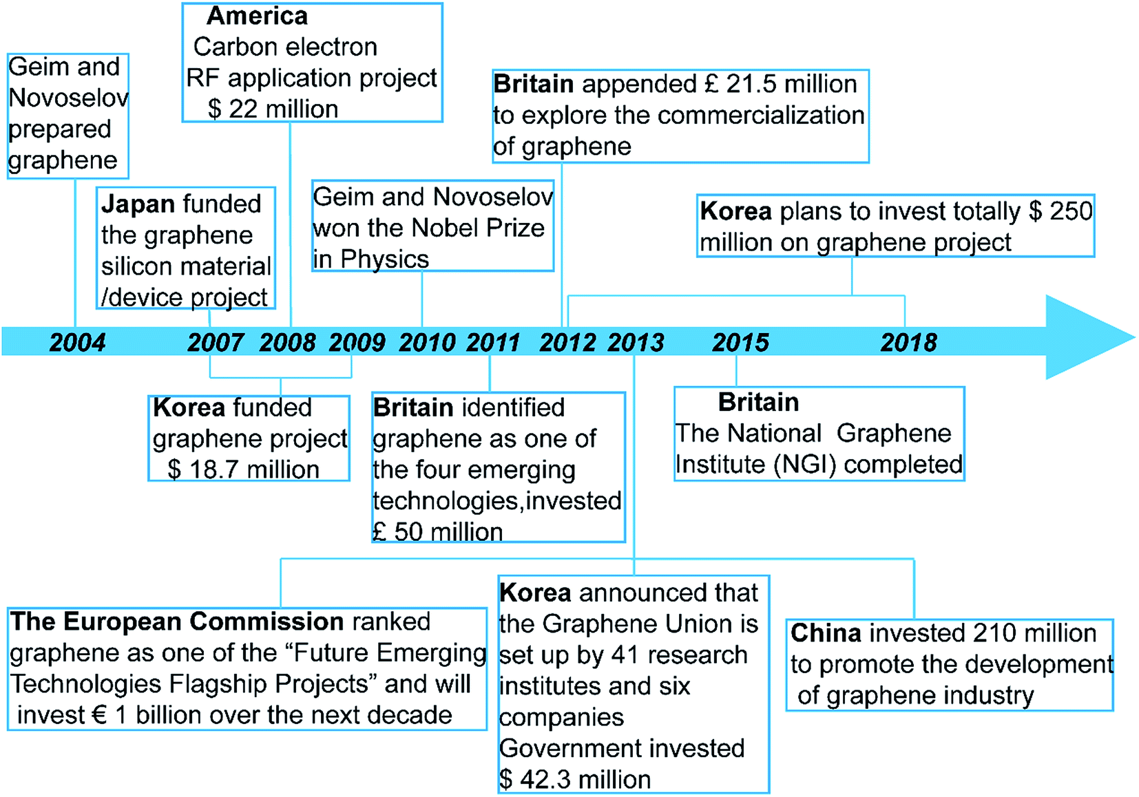 | ||
| Fig. 15 Investments in the field of graphene in different countries (ref. 211–218). | ||
European Commission ranked graphene as one of the “Future and Emerging Technologies Flagship Projects” in January 2013 and will provide €1 billion in funding in the next 10 years.212,213 More than 140 institutions from 23 countries had participated in the Graphene Flagship program at 2014. Graphene Flagship program will be divided into two parts: initial stage and stable stage. There will be €54 million of funding at the initial stage which is from October 1, 2013 to March 31, 2016 and the budget will be distributed among 126 academic and industrial research groups. In the stable stage (from Apr. 2016), it is expected to finance €50 million per year.
British identified graphene as one of the four emerging technologies in 2011. George Osborne, the UK's Chancellor of the Exchequer, announced that Britain would invest £50 million for graphene research and would take graphene from the British laboratory to the British factory floor.214,215 Among them, £38 million was used to set up a global hub for the research on the material at the University of Manchester. Many universities have also received funding, for instance, Cambridge University received more than £12 million for research in advanced flexible and light-based electronics. Imperial College London received about £4.5 million to research the use of graphene to get lightning-resistant and tougher aircraft components. In 2012, Britain appended £21.5 million to explore the commercialization of graphene. British announced that they will focus on the development of graphene and the British National Laboratory of Graphene will be completed in 2015.
South Korea funded $18.7 million for graphene project from 2007 to 2009. In 2013, Ministry of Trade, Industry and Energy of Korea announced that it will integrate the strength of Korean domestic research institutions and enterprises to promote commercial development of graphene and form graphene league in domestic. The graphene league included 41 research institutes and six companies. The government invested $42.3 million. South Korea planned to invest $200 million in graphene research from 2012 to 2018. Besides, many private companies like Samsung have made a significant contribution to it.211
Singapore is also working on graphene.216,217 In August of 2010, the Graphene Research Centre (GRC) at the National University of Singapore (NUS) was established with a start-up fund of $40 million from NUS. This centre aims to become a world leader in the field of 2D materials and plans to be a fully self-contained institute where experiment, theory and applications can be carried out simultaneously. GRC has also been supported by the National Research Foundation (NRF) of Singapore. It can obtain financing through competitive grant applications. For example, Prof. Castro Neto was awarded a $10 million Competitive Research Program (CRP) grant to study 2D crystals beyond graphene. In 2014, NRF of Singapore awarded NUS with a $50 million grant over the next 10 years in order to support the operational costs based on 2D materials. GRC also organizes a very important graphene conference—Recent Progress in Graphene Research which can bring together the most important Asian researchers in research of 2D materials and they can discuss the latest research progress.
The rise of the graphene has aroused great attention of Chinese government. Although China started late in the industrial production of LAG films, its development is very rapid. From 2007 to 2013, National Natural Science Foundation of China funded 1096 projects on graphene. In 2013, China invested 210 million to promote the development of graphene industry. China has successfully achieved the preparation of large single crystals,218,219 pure monolayers,220 three-dimensional graphene networks,221 and has invented a non-destructive electrochemical bubbling transfer method.218 Many other countries (America, Japan) have also invested in the graphene industry which will greatly promote the development of graphene industry.
Many enterprises have devoted to the industrial production of LAG films (Table 4).33 Bluestone Global Tech (in America) was founded in New York in 2011. This company is committed to the development of graphene technology and produces graphene films on various substrates (for example, Cu, PET or SiO2/Si). The largest films prepared on PET and Cu are 8 × 10 inch2 and 24 × 300 inch2, respectively. Sony (in Japan) developed a new method in 2012 using selective Joule heating of the copper foil to achieve the production of graphene films with a area of 100 m × 230 mm. Graphene Square (in Korea) which was established in January 2012 has developed a device for the fabrication of LAG films in size of A4. The largest graphene film they prepared and transferred to PET substrate is 30 inch (700 × 400 mm2).
| Company | Synthesis method | Main product | Basic properties | Applications |
|---|---|---|---|---|
| Bluestone Global Tech | CVD | Graphene films on Cu, SiO2/Si, PET | Maximum size: 24 × 300 inch2 on Cu, 8 × 10 inch2 on PET; sheet resistance: <150 Ω sq−1 at 95% transmittance | Field-effect transistors; touch panels |
| Sony Corporation | CVD | Graphene films on Cu, SiO2/Si, PET | Maximum size: 100 m × 230 mm, sheet resistance: <150 Ω sq−1 | Transparent conductive film; touch panels |
| Graphene Square | CVD | Films on Ni, Cu, PET, glass, SiO2 | Maximum size: 30 inch, sheet resistance: 125 Ω sq−1, transmittance: >97% | Touch screens |
| 2D Carbon Tech | CVD | On Cu, SiO2/Si, PET, glass | Maximum size: 45 × 55 cm2 on PET, monolayer >90%, sheet resistance: 200–400 Ω sq−1, transmittance: >85% | Touch panels |
| Power Booster | CVD | Films on Cu, PET | Maximum size: 7.5 m2 on Cu, carrier mobility: >3500 cm2 V−1 s−1, sheet resistance: <100 Ω sq−1 | Touch panels |
| Samsung | CVD | Films on Cu, PET, SiO2/Si | Maximum size: 30 inch, sheet resistance: 125 Ω sq−1, half-integer quantum Hall effect, transmittance: 97.4% | Transparent electrodes; touch screens |
Chongqing Institute of Green and Intelligent Technology, Chinese Academy of Sciences successfully prepared their first piece of monolayer graphene film in domestic in size of 15-inch on Cu substrate. The film can be transferred entirely to the flexible PET substrate and other substrates. 2D Carbon Tech was established in December 2011. The largest graphene film they fabricated on PET is 450 × 550 mm2. In January 2012, the company announced the first capacitive touch panel based on LAG. Power Booster was co-founded by China-US scientific research team in 2009. The company realized the production of 60-inch (1 m2) graphene films in 2012, 7.5 m2 films on copper and 3–20 inch touch panels in 2013.
5. Challenges and outlook
LAG has grown considerably in both area of applications and preparations in recent years. Many enterprises can produce high-quality LAG films for now, and these films can be used to fabricate flexible and wearable touch screens which can be applied in smart phones or tablets. Recently, ‘graphene phone’ has appeared on the market. Besides, LAG has exhibited great potentialities in the applications of transparent conducting electrodes, transistors, ultrathin electromagnetic shielding film, highly selective single molecule gas detection, desalination, DNA sequencing and osmotic energy production, etc. LAG is likely to be the next generation of “miracle material” in the future, but it may take a long time to be widely applied owing to many challenges, such as, the cost, the production volume, quality and transfer of LAG.33,222 The cost of graphene is a critical factor which can speed up or slow down the development of LAG. The price of per square centimeter graphene has fallen significantly compared with its initial price in the past few years, but it's still significantly higher than the price of traditional materials, for example, in 2008, the price of mechanically exfoliated graphene crystallite estimated by Geim was $1000 (ref. 223) and the price of graphene films in area of 10 × 10 cm2 produced by 2D Carbon Tech in 2014 is ¥1000, while the price of ITO conductive film is about 300–450 ¥ m−2. So the cost of graphene is still a big challenge and the development of graphene films will be resisted by the related manufacturers in some degree. Another challenge is how to achieve controllability of mass-production techniques in producing LAG films which are uniform, continuous, defect-free and the number of layers can be controlled. At the same time, it should realize the growth of LAG films on arbitrary substrates at low temperatures and realize intact, clean transfer of graphene films from metal substrates without destroying the substrates. How to achieve the application of LAG films in daily life as soon as possible is another challenge. Although the development of LAG faces many challenges, its development prospect is promising.Acknowledgements
This work was supported by the National Natural Science Foundation of China (51473097), (51003067), the Opening Project of State Key Laboratory of Polymer Materials Engineering (Sichuan University) (sklpme2014-3-14), and the Fundamental Research Funds for the Central Universities (2012SCU04A03).References
- A. K. Geim and K. S. Novoselov, Nat. Mater., 2007, 6, 183–191 CrossRef CAS PubMed
.
- C. N. R. Rao, A. K. Sood, K. S. Subrahmanyam and A. Govindaraj, Angew. Chem., Int. Ed., 2009, 48, 7752–7777 CrossRef CAS PubMed
- H. W. Kroto, J. R. Heath, S. C. O'Brien, R. F. Curl and R. E. Smalley, Nature, 1985, 318, 162–163 CrossRef CAS
- H. Shioyama and T. Akita, Carbon, 2003, 41, 179–181 CrossRef CAS
- H. E. Lim, Y. Miyata, R. Kitaura, Y. Nishimura, Y. Nishimoto, S. Irle, J. H. Warner, H. Kataura and H. Shinohara, Nat. Commun., 2013, 4, 2548 Search PubMed
- S. Kruss, A. J. Hilmer, J. Zhang, N. F. Reuel, B. Mu and M. S. Strano, Adv. Drug Delivery Rev., 2013, 65, 1933–1950 CrossRef CAS PubMed
- D. Yu and F. Liu, Nano Lett., 2007, 7, 3046–3050 CrossRef CAS PubMed
- M. Zhang and J. Li, Mater. Today, 2009, 12, 12–18 CrossRef CAS
- K. S. Novoselov, A. K. Geim, S. V. Morozov, D. Jiang, Y. Zhang, S. V. Dubonos, I. V. Grigorieva and A. A. Firsov, Science, 2004, 306, 666–669 CrossRef CAS PubMed
- K. S. Novoselov, A. K. Geim, S. V. Morozov, D. Jiang, M. I. Katsnelson, I. V. Grigorieva, S. V. Dubonos and A. A. Firsov, Nature, 2005, 438, 197–200 CrossRef CAS PubMed
- Y. Zhang, Y. W. Tan, H. L. Stormer and P. Kim, Nature, 2005, 438, 201–204 CrossRef CAS PubMed
- Y. Zhu, S. Murali, W. Cai, X. Li, J. W. Suk, J. R. Potts and R. S. Ruoff, Adv. Mater., 2010, 22, 3906–3924 CrossRef CAS PubMed
- C. Rao, K. Subrahmanyam, H. R. Matte, B. Abdulhakeem, A. Govindaraj, B. Das, P. Kumar, A. Ghosh and D. J. Late, Sci. Technol. Adv. Mater., 2010, 11, 054502 CrossRef
- C. Lee, X. Wei, J. W. Kysar and J. Hone, Science, 2008, 321, 385–388 CrossRef CAS PubMed
- A. A. Balandin, S. Ghosh, W. Bao, I. Calizo, D. Teweldebrhan, F. Miao and C. N. Lau, Nano Lett., 2008, 8, 902–907 CrossRef CAS PubMed
- F. Schedin, A. K. Geim, S. V. Morozov, E. W. Hill, P. Blake, M. I. Katsnelson and K. S. Novoselov, Nat. Mater., 2007, 6, 652–655 CrossRef CAS PubMed
- D. C. Elias, R. R. Nair, T. M. G. Mohiuddin, S. V. Morozov, P. Blake, M. P. Halsall, A. C. Ferrari, D. W. Boukhvalov, M. I. Katsnelson, A. K. Geim and K. S. Novoselov, Science, 2009, 323, 610–613 CrossRef CAS PubMed
- R. R. Nair, P. Blake, A. N. Grigorenko, K. S. Novoselov, T. J. Booth, T. Stauber, N. M. R. Peres and A. K. Geim, Science, 2008, 320, 1308 CrossRef CAS PubMed
- J. H. Chen, C. Jang, S. Xiao, M. Ishigami and M.
S. Fuhrer, Nat. Nanotechnol., 2008, 3, 206–209 CrossRef CAS PubMed
- C. Rao, K. Gopalakrishnan and A. Govindaraj, Nano Today, 2014, 9, 324–343 CrossRef CAS
- K. S. Subrahmanyam, L. S. Panchakarla, A. Govindaraj and C. N. R. Rao, J. Phys. Chem. C, 2009, 113, 4257–4259 CAS
- U. A. Palnitkar, R. V. Kashid, M. A. More, D. S. Joag, L. S. Panchakarla and C. N. R. Rao, Appl. Phys. Lett., 2010, 97, 063102 CrossRef
- D. J. Late, A. Ghosh, K. S. Subrahmanyam, L. S. Panchakarla, S. B. Krupanidhi and C. N. R. Rao, Solid State Commun., 2010, 150, 734–738 CrossRef CAS
- C. N. R. Rao, K. S. Subrahmanyam, H. S. S. R. Matte, B. Abdulhakeem, A. Govindaraj, D. Barun, K. Prashant, G. Anupama and J. L. Dattatray, Sci. Technol. Adv. Mater., 2010, 11, 054502 CrossRef
- C. N. R. Rao, K. S. Subrahmanyam, H. S. S. Ramakrishna Matte and A. Govindaraj, Mod. Phys. Lett. B, 2011, 25, 427–451 CrossRef CAS
- E. P. Randviir, D. A. C. Brownson and C. E. Banks, Mater. Today, 2014, 17, 426–432 CrossRef CAS
- P. R. Somani, S. P. Somani and M. Umeno, Chem. Phys. Lett., 2006, 430, 56–59 CrossRef CAS
- A. N. Obraztsov, E. A. Obraztsova, A. V. Tyurnina and A. A. Zolotukhin, Carbon, 2007, 45, 2017–2021 CrossRef CAS
- G. Eda, G. Fanchini and M. Chhowalla, Nat. Nanotechnol., 2008, 3, 270–274 CrossRef CAS PubMed
- X. Li, W. Cai, J. An, S. Kim, J. Nah, D. Yang, R. Piner, A. Velamakanni, I. Jung, E. Tutuc, S. K. Banerjee, L. Colombo and R. S. Ruoff, Science, 2009, 324, 1312–1314 CrossRef CAS PubMed
- X. Li, Y. Zhu, W. Cai, M. Borysiak, B. Han, D. Chen, R. D. Piner, L. Colombo and R. S. Ruoff, Nano Lett., 2009, 9, 4359–4363 CrossRef CAS PubMed
- S. Bae, H. Kim, Y. Lee, X. Xu, J.-S. Park, Y. Zheng, J. Balakrishnan, T. Lei, H. Ri Kim, Y. I. Song, Y.-J. Kim, K. S. Kim, B. Ozyilmaz, J.-H. Ahn, B. H. Hong and S. Iijima, in Nature Nanotechnology, Nature Publishing Group, 2010, vol. 5, pp. 574–578 Search PubMed
- W. Ren and H. M. Cheng, Nat. Nanotechnol., 2014, 9, 726–730 CrossRef CAS PubMed
- J. Kim, M. Ishihara, Y. Koga, K. Tsugawa, M. Hasegawa and S. Iijima, Appl. Phys. Lett., 2011, 98, 091502 CrossRef
- J. Wang, M. Liang, Y. Fang, T. Qiu, J. Zhang and L. Zhi, Adv. Mater., 2012, 24, 2874–2878 CrossRef CAS PubMed
- T. Yamada, M. Ishihara, J. Kim, M. Hasegawa and S. Iijima, Carbon, 2012, 50, 2615–2619 CrossRef CAS
- T. Kobayashi, M. Bando, N. Kimura, K. Shimizu, K. Kadono, N. Umezu, K. Miyahara, S. Hayazaki, S. Nagai, Y. Mizuguchi, Y. Murakami and D. Hobara, Appl. Phys. Lett., 2013, 102, 023112 CrossRef
- J. Liu, P. Li, Y. Chen, Z. Wang, J. He, H. Tian, F. Qi, B. Zheng, J. Zhou, W. Lin and W. Zhang, J. Alloys Compd., 2014, 615, 415–418 CrossRef CAS
- J. Ryu, Y. Kim, D. Won, N. Kim, J. S. Park, E.-K. Lee, D. Cho, S.-P. Cho, S. J. Kim, G. H. Ryu, H.-A. S. Shin, Z. Lee, B. H. Hong and S. Cho, ACS Nano, 2013, 8, 950–956 CrossRef PubMed
- G. Eda and M. Chhowalla, Adv. Mater., 2010, 22, 2392–2415 CrossRef CAS PubMed
- R. Muñoz and C. Gómez-Aleixandre, Chem. Vap. Deposition, 2013, 19, 297–322 CrossRef
- Y. Yang, Z. Liu, Z. Yin, Z. Du, L. Xie, M. Yi, J. Liu and W. Huang, RSC Adv., 2014, 4, 55671–55676 RSC
- J. Wang, Z. Fang, H. Zhu, B. Gao, S. Garner, P. Cimo, Z. Barcikowski, A. Mignerey and L. Hu, Thin Solid Films, 2014, 556, 13–17 CrossRef CAS
- J. Xie, H. Wang, H. Bai, P. Yang, M. Shi, P. Guo, C. Wang, W. Yang and H. Song, ACS Appl. Mater. Interfaces, 2012, 4, 2891–2896 CAS
- S. K. Kalpathy, L. F. Francis and S. Kumar, J. Colloid Interface Sci., 2012, 383, 155–166 CrossRef CAS PubMed
- H. A. Becerril, J. Mao, Z. Liu, R. M. Stoltenberg, Z. Bao and Y. Chen, ACS Nano, 2008, 2, 463–470 CrossRef CAS PubMed
- J. T. Robinson, M. Zalalutdinov, J. W. Baldwin, E. S. Snow, Z. Wei, P. Sheehan and B. H. Houston, Nano Lett., 2008, 8, 3441–3445 CrossRef CAS PubMed
- J. T. Robinson, F. K. Perkins, E. S. Snow, Z. Wei and P. E. Sheehan, Nano Lett., 2008, 8, 3137–3140 CrossRef CAS PubMed
- S. Pang, H. N. Tsao, X. Feng and K. Müllen, Adv. Mater., 2009, 21, 3488–3491 CrossRef CAS
- H. Yamaguchi, G. Eda, C. Mattevi, H. Kim and M. Chhowalla, ACS Nano, 2010, 4, 524–528 CrossRef CAS PubMed
- J. Wu, M. Agrawal, H. A. Becerril, Z. Bao, Z. Liu, Y. Chen and P. Peumans, ACS Nano, 2010, 4, 43–48 CrossRef CAS PubMed
- H. Chang, G. Wang, A. Yang, X. Tao, X. Liu, Y. Shen and Z. Zheng, Adv. Funct. Mater., 2010, 20, 2893–2902 CrossRef CAS
- H. B. Sun, J. Yang, Y. Z. Zhou, N. Zhao and D. Li, Mater. Technol., 2014, 29, 14–20 CrossRef CAS
- X. Wang, L. Zhi and K. Müllen, Nano Lett., 2008, 8, 323–327 CrossRef CAS PubMed
- H. G. Jeon, Y. H. Huh, S. H. Yun, K. W. Kim, S. S. Lee, J. Lim, K.-S. An and B. Park, J. Mater. Chem. C, 2014, 2, 2622–2634 RSC
- X. Cao, D. Qi, S. Yin, J. Bu, F. Li, C. F. Goh, S. Zhang and X. Chen, Adv. Mater., 2013, 25, 2957–2962 CrossRef CAS PubMed
- G. Eda, Y.-Y. Lin, S. Miller, C.-W. Chen, W.-F. Su and M. Chhowalla, Appl. Phys. Lett., 2008, 92, 233305 CrossRef
- S. Y. Oh, S. H. Kim, Y. S. Chi and T. J. Kang, Appl. Surf. Sci., 2012, 258, 8837–8844 CrossRef CAS
- S. H. Park and H. S. Kim, Nanotechnology, 2015, 26, 205601 CrossRef PubMed
- M. Yang, S. Ko, J. S. Im and B. G. Choi, J. Power Sources, 2015, 288, 76–81 CrossRef CAS
- Y.-K. Kim and D.-H. Min, Chem.–Eur. J., 2015, 21, 7217–7223 CrossRef CAS PubMed
- P. Du, X. Hu, C. Yi, H. C. Liu, P. Liu, H.-L. Zhang and X. Gong, Adv. Funct. Mater., 2015, 25, 2420–2427 CrossRef CAS
- D. D. Nguyen, Y.-T. Lai and N.-H. Tai, Diamond Relat. Mater., 2014, 47, 1–6 CrossRef CAS
- H. X. Kong, Curr. Opin. Solid State Mater. Sci., 2013, 17, 31–37 CrossRef CAS
- L. Huang, Y. Wang, J. Tang, H. Wang, H. Wang, J. Qiu, Y. Wang, J. Liu and J. Liu, Int. J. Electrochem. Sci., 2012, 7, 11068–11075 CAS
- U. Khan, I. O'Connor, Y. K. Gun'ko and J. N. Coleman, Carbon, 2010, 48, 2825–2830 CrossRef CAS
- J. Geng and H.-T. Jung, J. Phys. Chem. C, 2010, 114, 8227–8234 CAS
- M. Kim, W. J. Hyun, S. C. Mun and O. O. Park, J. Phys.: Conf. Ser., 2015, 602, 012027 CrossRef
- J.-J. Shao, W. Lv and Q.-H. Yang, Adv. Mater., 2014, 26, 5586–5612 CrossRef CAS PubMed
- F. Kim, L. J. Cote and J. Huang, Adv. Mater., 2010, 22, 1954–1958 CrossRef CAS PubMed
- J. Kim, L. J. Cote, F. Kim, W. Yuan, K. R. Shull and J. Huang, J. Am. Chem. Soc., 2010, 132, 8180–8186 CrossRef CAS PubMed
- K. Min, T. H. Han, J. Kim, J. Jung, C. Jung, S. M. Hong and C. M. Koo, J. Colloid Interface Sci., 2012, 383, 36–42 CrossRef CAS PubMed
- G. Xin, H. Sun, T. Hu, H. R. Fard, X. Sun, N. Koratkar, T. Borca-Tasciuc and J. Lian, Adv. Mater., 2014, 26, 4521–4526 CrossRef CAS PubMed
- R. K. Layek, A. K. Das, M. U. Park, N. H. Kim and J. H. Lee, J. Mater. Chem. A, 2014, 2, 12158–12161 CAS
- M. Beidaghi, Z. Wang, L. Gu and C. Wang, J. Solid State Electrochem., 2012, 16, 3341–3348 CrossRef CAS
- S. Gilje, S. Han, M. Wang, K. L. Wang and R. B. Kaner, Nano Lett., 2007, 7, 3394–3398 CrossRef CAS PubMed
- V. H. Pham, T. V. Cuong, S. H. Hur, E. W. Shin, J. S. Kim, J. S. Chung and E. J. Kim, Carbon, 2010, 48, 1945–1951 CrossRef CAS
- N.-W. Pu, C.-A. Wang, Y.-M. Liu, Y. Sung, D.-S. Wang and M.-D. Ger, J. Taiwan Inst. Chem. Eng., 2012, 43, 140–146 CrossRef CAS
- X. Wu, F. Li, W. Wu and T. Guo, Appl. Surf. Sci., 2014, 295, 214–218 CrossRef CAS
- Y.-J. Jeon, J.-M. Yun, D.-Y. Kim, S.-I. Na and S.-S. Kim, Appl. Surf. Sci., 2014, 296, 140–146 CrossRef CAS
- Y. Meng, X.-B. Xu, H. Li, Y. Wang, E.-X. Ding, Z.-C. Zhang and H.-Z. Geng, Carbon, 2014, 70, 103–110 CrossRef CAS
- B. Dan, G. C. Irvin and M. Pasquali, ACS Nano, 2009, 3, 835–843 CrossRef CAS PubMed
- L. Hu, H. S. Kim, J.-Y. Lee, P. Peumans and Y. Cui, ACS Nano, 2010, 4, 2955–2963 CrossRef CAS PubMed
- C.-H. Liu and X. Yu, Nanoscale Res. Lett., 2011, 6, 75 CrossRef PubMed
- Y. Lou, G. Liu, S. Liu, J. Shen and W. Jin, Appl. Surf. Sci., 2014, 307, 631–637 CrossRef CAS
- H. Qiu, L. Zeng, T. Lan, X. Ding and M. Wei, J. Mater. Chem. A, 2015, 3, 1619–1623 CAS
- P. Meenakshi, R. Karthick, M. Selvaraj and S. Ramu, Sol. Energy Mater. Sol. Cells, 2014, 128, 264–269 CrossRef CAS
- Y. A. Samad, Y. Li, S. M. Alhassan and K. Liao, ACS Appl. Mater. Interfaces, 2015, 7, 9195–9202 CAS
- A. A. Shabaneh, S. H. Girei, P. T. Arasu, W. B. W. A. Rahman, A. A. A. Bakar, A. Z. Sadek, H. N. Lim, N. M. Huang and M. H. Yaacob, Opt. Commun., 2014, 331, 320–324 CrossRef CAS
- K. Goh, L. Setiawan, L. Wei, R. Si, A. G. Fane, R. Wang and Y. Chen, J. Membr. Sci., 2015, 474, 244–253 CrossRef CAS
- C. Zhao, X. Lu, C. Zanden and J. Liu, Biomed. Mater., 2015, 10, 015019 CrossRef PubMed
- F. A. Jumeri, H. N. Lim, Z. Zainal, N. M. Huang and A. Pandikumar, Ceram. Int., 2014, 40, 15159–15165 CrossRef CAS
- Y. Niu, X. Zhang, W. Pan, J. Zhao and Y. Li, RSC Adv., 2014, 4, 7511–7515 RSC
- Y. Niu, J. Zhao, X. Zhang, X. Wang, J. Wu, Y. Li and Y. Li, Appl. Phys. Lett., 2012, 101, 181903 CrossRef
- Y. F. Bai, Y. F. Zhang, A. W. Zhou, H. W. Li, Y. Zhang, J. H. Luong and H. F. Cui, Nanotechnology, 2014, 25, 405601 CrossRef PubMed
- J.-J. Shao, W. Lv, Q. Guo, C. Zhang, Q. Xu, Q.-H. Yang and F. Kang, Chem. Commun., 2012, 48, 3706–3708 RSC
- J. Zhao, S. Pei, W. Ren, L. Gao and H.-M. Cheng, ACS Nano, 2010, 4, 5245–5252 CrossRef CAS PubMed
- P. Zhang, X. Zhang, S. Zhang, X. Lu, Q. Li, Z. Su and G. Wei, J. Mater. Chem. B, 2013, 1, 6525–6531 RSC
- S. Z. Moghaddam, S. Sabury and F. Sharif, RSC Adv., 2014, 4, 8711–8719 RSC
- F. Chen, S. Liu, J. Shen, L. Wei, A. Liu, M. B. Chan-Park and Y. Chen, Langmuir, 2011, 27, 9174–9181 CrossRef CAS PubMed
- J. Xin, B. Xie, Y. Li, J. Shang, Y. Qiu, L. Liu, S. Zhao, L. Fan and R. Zhang, Compos. Interfaces, 2014, 21, 623–630 CrossRef CAS
- S. Biswas and L. T. Drzal, Nano Lett., 2009, 9, 167–172 Search PubMed.
- K. Arapov, A. Goryachev, G. d. With and H. Friedrich, Synth. Met., 2015, 201, 67–75 CrossRef CAS
- Q. Liu, M. He, X. Xu, L. Zhang and J. Yu, New J. Chem., 2013, 37, 181–187 RSC
- T. Yang, J. Yang, L. Shi, E. Mader and Q. Zheng, RSC Adv., 2015, 5, 23650–23657 RSC
- X. Lin, J. Jia, N. Yousefi, X. Shen and J.-K. Kim, J. Mater. Chem. C, 2013, 1, 6869–6877 RSC
- Q.-b. Zheng, L.-f. Shi and J.-h. Yang, Trans. Nonferrous Met. Soc. China, 2012, 22, 2504–2511 CrossRef CAS
- Q. Zheng, W. H. Ip, X. Lin, N. Yousefi, K. K. Yeung, Z. Li and J.-K. Kim, ACS Nano, 2011, 5, 6039–6051 CrossRef CAS PubMed
- D. D. Kulkarni, I. Choi, S. S. Singamaneni and V. V. Tsukruk, ACS Nano, 2010, 4, 4667–4676 CrossRef CAS PubMed
- V. Divakar Botcha, G. Singh, P. K. Narayanam, D. S. Sutar, S. S. Talwar, R. S. Srinivasa and S. S. Major, AIP Conf. Proc., 2012, 1447, 327–328 CrossRef CAS
- X. Li, G. Zhang, X. Bai, X. Sun, X. Wang, E. Wang and H. Dai, Nat. Nanotechnol., 2008, 3, 538–542 CrossRef CAS PubMed
- T. H. Han, J. Nanosci. Nanotechnol., 2015, 15, 1191–1194 CrossRef CAS PubMed
- L. J. Cote, F. Kim and J. Huang, J. Am. Chem. Soc., 2008, 131, 1043–1049 CrossRef PubMed
- L. J. Cote, J. Kim, Z. Zhang, C. Sun and J. Huang, Soft Matter, 2010, 6, 6096–6101 RSC
- X. Zhang, H. Li and F. Ding, Adv. Mater., 2014, 26, 5488–5495 CrossRef PubMed
- B.-J. Lee and G.-H. Jeong, Appl. Phys. A: Mater. Sci. Process., 2014, 116, 15–24 CrossRef CAS
- K. Yan, L. Fu, H. Peng and Z. Liu, Acc. Chem. Res., 2013, 46, 2263–2274 CrossRef CAS PubMed
- A. Malesevic, R. Vitchev, K. Schouteden, A. Volodin, L. Zhang, G. V. Tendeloo, A. Vanhulsel and C. V. Haesendonck, Nanotechnology, 2008, 19, 305604 CrossRef PubMed
- A. Dato, V. Radmilovic, Z. Lee, J. Phillips and M. Frenklach, Nano Lett., 2008, 8, 2012–2016 CrossRef CAS PubMed
- R. Vitchev, A. Malesevic, R. H. Petrov, R. Kemps, M. Mertens, A. Vanhulsel and C. Van Haesendonck, Nanotechnology, 2010, 21, 095602 CrossRef PubMed
- Y. Kim, W. Song, S. Y. Lee, C. Jeon, W. Jung, M. Kim and C. Y. Park, Appl. Phys. Lett., 2011, 98, 263106–2631063 CrossRef PubMed
- G. Kalita, K. Wakita and M. Umeno, RSC Adv., 2012, 2, 2815–2820 RSC
- G. Kalita, M. S. Kayastha, H. Uchida, K. Wakita and M. Umeno, RSC Adv., 2012, 2, 3225–3230 RSC
- G. Kalita, S. Sharma, K. Wakita, M. Umeno, Y. Hayashi and M. Tanemura, Phys. Status Solidi A, 2012, 209, 2510–2513 CrossRef CAS
- C. Wang, Y. Zhou, L. He, T.-W. Ng, G. Hong, Q.-H. Wu, F. Gao, C.-S. Lee and W. Zhang, Nanoscale, 2013, 5, 600–605 RSC
- M. Hiramatsu, M. Naito, H. Kondo and M. Hori, Jpn. J. Appl. Phys., 2013, 52, 01AK04 CrossRef
- A. Kumar, A. A. Voevodin, D. Zemlyanov, D. N. Zakharov and T. S. Fisher, Carbon, 2012, 50, 1546–1553 CrossRef CAS
- A. Kumar, A. A. Voevodin, R. Paul, I. Altfeder, D. Zemlyanov, D. N. Zakharov and T. S. Fisher, Thin Solid Films, 2013, 528, 269–273 CrossRef CAS
- T. Yamada, J. Kim, M. Ishihara and M. Hasegawa, J. Phys. D: Appl. Phys., 2013, 46, 063001 CrossRef
- T. Yamada, M. Ishihara and M. Hasegawa, Thin Solid Films, 2013, 532, 89–93 CrossRef CAS
- Y. Okigawa, K. Tsugawa, T. Yamada, M. Ishihara and M. Hasegawa, Appl. Phys. Lett., 2013, 103, 153106 CrossRef
- R. Kato, K. Tsugawa, T. Yamada, M. Ishihara and M. Hasegawa, Jpn. J. Appl. Phys., 2014, 53, 015505 CrossRef
- Y. Okigawa, R. Kato, T. Yamada, M. Ishihara and M. Hasegawa, Carbon, 2015, 82, 60–66 CrossRef CAS
- H. J. Park, B. W. Ahn, T. Y. Kim, J. W. Lee, Y. H. Jung, Y. S. Choi, Y. I. Song and S. J. Suh, Thin Solid Films, 2015, 587, 8–13 CrossRef CAS
- T. Yamada, M. Ishihara and M. Hasegawa, Appl. Phys. Express, 2013, 6, 115102 CrossRef
- Q. Yu, J. Lian, S. Siriponglert, H. Li, Y. P. Chen and S.-S. Pei, Appl. Phys. Lett., 2008, 93, 113103 CrossRef
- K. E. Whitener and P. E. Sheehan, Diamond Relat. Mater., 2014, 46, 25–34 CrossRef CAS
- H. Huang, Y. Ying and X. Peng, J. Mater. Chem. A, 2014, 2, 13772–13782 CAS
- T. Humplik, J. Lee, S. C. O'Hern, B. A. Fellman, M. A. Baig, S. F. Hassan, M. A. Atieh, F. Rahman, T. Laoui, R. Karnik and E. N. Wang, Nanotechnology, 2011, 22, 292001 CrossRef CAS PubMed
- M. Hu and B. Mi, Environ. Sci. Technol., 2013, 47, 3715–3723 CrossRef CAS PubMed
- W. Choi, J. Choi, J. Bang and J. H. Lee, ACS Appl. Mater. Interfaces, 2013, 5, 12510–12519 CAS
- J.-G. Gai, X.-L. Gong, W.-W. Wang, X. Zhang and W.-L. Kang, J. Mater. Chem. A, 2014, 2, 4023 CAS
- J. Azamat, A. Khataee and S. W. Joo, J. Mol. Graphics Modell., 2014, 53, 112–117 CrossRef CAS PubMed
- B. Liang, W. Zhan, G. Qi, S. Lin, Q. Nan, Y. Liu, B. Cao and K. Pan, J. Mater. Chem. A, 2015, 3, 5140–5147 CAS
- K. A. Mahmoud, B. Mansoor, A. Mansour and M. Khraisheh, Desalination, 2015, 356, 208–225 CrossRef CAS
- P. S. Goh and A. F. Ismail, Desalination, 2015, 356, 115–128 CrossRef CAS
- L. He, L. F. Dumée, C. Feng, L. Velleman, R. Reis, F. She, W. Gao and L. Kong, Desalination, 2015, 365, 126–135 CrossRef CAS
- A. Subramani and J. G. Jacangelo, Water Res., 2015, 75, 164–187 CrossRef CAS PubMed
- S. Daer, J. Kharraz, A. Giwa and S. W. Hasan, Desalination, 2015, 367, 37–48 CrossRef CAS
- S. P. Surwade, S. N. Smirnov, I. V. Vlassiouk, R. R. Unocic, G. M. Veith, S. Dai and S. M. Mahurin, Nat. Nanotechnol., 2015, 10, 459–464 CrossRef CAS PubMed
- S. C. O'Hern, D. Jang, S. Bose, J. C. Idrobo, Y. Song, T. Laoui, J. Kong and R. Karnik, Nano Lett., 2015, 15, 3254–3260 CrossRef PubMed
- D. Cohen-Tanugi and J. C. Grossman, Nano Lett., 2012, 12, 3602–3608 CrossRef CAS PubMed
- A. Nicolaï, B. G. Sumpter and V. Meunier, Phys. Chem. Chem. Phys., 2014, 16, 8646–8654 RSC
- D. Cohen-Tanugi and J. C. Grossman, J. Chem. Phys., 2014, 141, 074704 CrossRef PubMed
- M. E. Suk and N. R. Aluru, J. Phys. Chem. Lett., 2010, 1, 1590–1594 CrossRef CAS
- I. Akin, E. Zor, H. Bingol and M. Ersoz, J. Phys. Chem. B, 2014, 118, 5707–5716 CrossRef CAS PubMed
- F. Perreault, A. F. de Faria and M. Elimelech, Chem. Soc. Rev., 2015, 44, 5861–5896 RSC
- K. Sint, B. Wang and P. Král, J. Am. Chem. Soc., 2008, 130, 16448–16449 CrossRef CAS PubMed
- D. Konatham, J. Yu, T. A. Ho and A. Striolo, Langmuir, 2013, 29, 11884–11897 CrossRef CAS PubMed
- D. Cohen-Tanugi and J. C. Grossman, Nano Lett., 2014, 14, 6171–6178 CrossRef CAS PubMed
- D. Cohen-Tanugi and J. C. Grossman, Desalination, 2015, 366, 59–70 CrossRef CAS
- M. Drndić, Nat. Nanotechnol., 2014, 9, 737 Search PubMed.
- S. Garaj, W. Hubbard, A. Reina, J. Kong, D. Branton and J. A. Golovchenko, Nature, 2010, 467, 190–193 CrossRef CAS PubMed
- C. A. Merchant, K. Healy, M. Wanunu, V. Ray, N. Peterman, J. Bartel, M. D. Fischbein, K. Venta, Z. Luo, A. T. Johnson and M. Drndic, Nano Lett., 2010, 10, 2915–2921 CrossRef CAS PubMed
- G. F. Schneider, S. W. Kowalczyk, V. E. Calado, G. Pandraud, H. W. Zandbergen, L. M. Vandersypen and C. Dekker, Nano Lett., 2010, 10, 3163–3167 CrossRef CAS PubMed
- Z. Zhang, J. Shen, H. Wang, Q. Wang, J. Zhang, L. Liang, H. Ågren and Y. Tu, J. Phys. Chem. Lett., 2014, 5, 1602–1607 CrossRef CAS PubMed
- D. B. Wells, M. Belkin, J. Comer and A. Aksimentiev, Nano Lett., 2012, 12, 4117–4123 CrossRef CAS PubMed
- M. Zwolak and M. Di Ventra, Nano Lett., 2005, 5, 421–424 CrossRef CAS PubMed
- M. Xu, R. G. Endres and Y. Arakawa, Small, 2007, 3, 1539–1543 CrossRef CAS PubMed
- M. Xu, D. Fujita and N. Hanagata, Small, 2009, 5, 2638–2649 CrossRef CAS PubMed
- S. M. Avdoshenko, D. Nozaki, C. Gomes da Rocha, J. W. González, M. H. Lee, R. Gutierrez and G. Cuniberti, Nano Lett., 2013, 13, 1969–1976 CrossRef CAS PubMed
- W. Lv, M. Chen and R. a. Wu, Soft Matter, 2013, 9, 960–966 RSC
- R. F. Service, Science, 2006, 311, 1544–1546 CrossRef CAS PubMed
- A. Kumar, K. B. Park, H. M. Kim and K. B. Kim, Nanotechnology, 2013, 24, 495503 CrossRef PubMed
- H. W. C. Postma, Nano Lett., 2010, 10, 420–425 CrossRef CAS PubMed
- T. Nelson, B. Zhang and O. V. Prezhdo, Nano Lett., 2010, 10, 3237–3242 CrossRef CAS PubMed
- S. K. Min, W. Y. Kim, Y. Cho and K. S. Kim, Nat. Nanotechnol., 2011, 6, 162–165 CrossRef CAS PubMed
- G. T. Feliciano, C. Sanz-Navarro, M. D. Coutinho-Neto, P. Ordejón, R. H. Scheicher and A. R. Rocha, Phys. Rev. Appl., 2015, 3, 034003 CrossRef
- L. Liang, Z. Zhang, J. Shen, K. Zhe, Q. Wang, T. Wu, H. Agren and Y. Tu, RSC Adv., 2014, 4, 50494–50502 RSC
- M. Xu, Y. Gao, X. Yang and H. Chen, Chin. Sci. Bull., 2012, 57, 3000–3009 CrossRef CAS
- J. Shendure and H. Ji, Nat. Biotechnol., 2008, 26, 1135–1145 CrossRef CAS PubMed
- D. Branton, D. W. Deamer, A. Marziali, H. Bayley, S. A. Benner, T. Butler, M. Di Ventra, S. Garaj, A. Hibbs, X. Huang, S. B. Jovanovich, P. S. Krstic, S. Lindsay, X. S. Ling, C. H. Mastrangelo, A. Meller, J. S. Oliver, Y. V. Pershin, J. M. Ramsey, R. Riehn, G. V. Soni, V. Tabard-Cossa, M. Wanunu, M. Wiggin and J. A. Schloss, Nat. Biotechnol., 2008, 26, 1146–1153 CrossRef CAS PubMed
- D.-e. Jiang, V. R. Cooper and S. Dai, Nano Lett., 2009, 9, 4019–4024 CrossRef CAS PubMed
- J. Schrier, J. Phys. Chem. Lett., 2010, 1, 2284–2287 CrossRef CAS
- S. Blankenburg, M. Bieri, R. Fasel, K. Müllen, C. A. Pignedoli and D. Passerone, Small, 2010, 6, 2266–2271 CrossRef CAS PubMed
- H. Du, J. Li, J. Zhang, G. Su, X. Li and Y. Zhao, J. Phys. Chem. C, 2011, 115, 23261–23266 CAS
- A. W. Hauser and P. Schwerdtfeger, J. Phys. Chem. Lett., 2012, 3, 209–213 CrossRef CAS
- M. Hankel, Y. Jiao, A. Du, S. K. Gray and S. C. Smith, J. Phys. Chem. C, 2012, 116, 6672–6676 CAS
- M. Shan, Q. Xue, N. Jing, C. Ling, T. Zhang, Z. Yan and J. Zheng, Nanoscale, 2012, 4, 5477–5482 RSC
- S. P. Koenig, L. Wang, J. Pellegrino and J. S. Bunch, Nat. Nanotechnol., 2012, 7, 728–732 CrossRef CAS PubMed
- X. Qin, Q. Meng, Y. Feng and Y. Gao, Surf. Sci., 2013, 607, 153–158 CrossRef CAS
- S. Jungthawan, P. Reunchan and S. Limpijumnong, Carbon, 2013, 54, 359–364 CrossRef CAS
- J. Lee and N. R. Aluru, J. Membr. Sci., 2013, 428, 546–553 CrossRef CAS
- H. W. Kim, H. W. Yoon, S.-M. Yoon, B. M. Yoo, B. K. Ahn, Y. H. Cho, H. J. Shin, H. Yang, U. Paik, S. Kwon, J.-Y. Choi and H. B. Park, Science, 2013, 342, 91–95 CrossRef CAS PubMed
- H. Li, Z. Song, X. Zhang, Y. Huang, S. Li, Y. Mao, H. J. Ploehn, Y. Bao and M. Yu, Science, 2013, 342, 95–98 CrossRef CAS PubMed
- G. Lei, C. Liu, H. Xie and F. Song, Chem. Phys. Lett., 2014, 599, 127–132 CrossRef CAS
- H. Liu, Z. Chen, S. Dai and D.-e. Jiang, J. Solid State Chem., 2015, 224, 2–6 CrossRef CAS
- H. Liu, S. Dai and D.-e. Jiang, Solid State Commun., 2013, 175–176, 101–105 CrossRef CAS
- I. S. Chae, J. H. Lee, J. Hong, Y. S. Kang and S. W. Kang, Chem. Eng. J., 2014, 251, 343–347 CrossRef CAS
- H. Koolivand, A. Sharif, M. Kashani, M. Karimi, M. Salooki and M. Semsarzadeh, J. Polym. Res., 2014, 21, 1–12 CAS
- H. W. Kim, H. W. Yoon, B. M. Yoo, J. S. Park, K. L. Gleason, B. D. Freeman and H. B. Park, Chem. Commun., 2014, 50, 13563–13566 RSC
- J. Shen, G. Liu, K. Huang, W. Jin, K.-R. Lee and N. Xu, Angew. Chem., Int. Ed., 2015, 54, 578–582 Search PubMed
- R. S. Norman, Science, 1974, 186, 350–352 CAS
- R. L. McGinnis and M. Elimelech, Environ. Sci. Technol., 2008, 42, 8625–8629 CrossRef CAS PubMed
- R. D. Cusick, Y. Kim and B. E. Logan, Science, 2012, 335, 1474–1477 CrossRef CAS PubMed
- B. E. Logan and M. Elimelech, Nature, 2012, 488, 313–319 CrossRef CAS PubMed
- R. E. Pattle, Nature, 1954, 174, 660 CrossRef CAS
- S. Zhao, L. Zou, C. Y. Tang and D. Mulcahy, J. Membr. Sci., 2012, 396, 1–21 CrossRef CAS
- F. Sanger, G. M. Air, B. G. Barrell, N. L. Brown, A. R. Coulson, J. C. Fiddes, C. A. Hutchison, P. M. Slocombe and M. Smith, Nature, 1977, 265, 687–695 CrossRef CAS PubMed
- F. Sanger, S. Nicklen and A. R. Coulson, Proc. Natl. Acad. Sci. U. S. A., 1977, 74, 5463–5467 CrossRef CAS
- J. Ribeiro-Soares and M. Dresselhaus, Braz. J. Phys., 2014, 44, 278–282 CrossRef
- http://www.observatorioplastico.com/detalle_noticia.php?no_id=360448
- Editorial, Nat. Nanotechnol., 2014, 9, 725 Search PubMed.
- Q. Tannock, Nat. Mater., 2011, 11, 2 CrossRef PubMed
- http://www.theguardian.com/science/2012/dec/27/super-material-graphene-george-osborne
- A. H. Castro Neto, Asia Pacific Physics Newsletter, 2013, 02, 60–65 CrossRef
- http://www.graphene.nus.edu.sg/content/graphene-centre
- L. Gao, W. Ren, H. Xu, L. Jin, Z. Wang, T. Ma, L.-P. Ma, Z. Zhang, Q. Fu, L.-M. Peng, X. Bao and H.-M. Cheng, Nat. Commun., 2012, 3, 699 CrossRef PubMed
- T. Ma, W. Ren, Z. Liu, L. Huang, L.-P. Ma, X. Ma, Z. Zhang, L.-M. Peng and H.-M. Cheng, ACS Nano, 2014, 8, 12806–12813 CrossRef CAS PubMed
- B. Y. Dai, L. Fu, Z. Y. Zou, M. Wang, H. T. Xu, S. Wang and Z. F. Liu, Nat. Commun., 2011, 2, 522 CrossRef PubMed
- Z. Chen, W. Ren, L. Gao, B. Liu, S. Pei and H.-M. Cheng, Nat. Mater., 2011, 10, 424–428 CrossRef CAS PubMed
- A. Zurutuza and C. Marinelli, Nat. Nanotechnol., 2014, 9, 730–734 CrossRef CAS PubMed
- A. K. Geim and P. Kim, Sci. Am., 2008, 298, 90–97 CrossRef CAS PubMed
| This journal is © The Royal Society of Chemistry 2016 |