David E. Motaung*a,
Ioannis Kortidisc,
Gugu H. Mhlongoa,
Mart-Mari Duvenhageb,
Hendrik. C. Swartb,
George Kiriakidisc and
Suprakas Sinha Raya
aDST/CSIR National Centre for Nano-Structured Materials, Council for Scientific and Industrial Research, Pretoria 0001, South Africa. E-mail: dmotaung@csir.co.za; Tel: +27 12 841 4775
bDepartment of Physics, University of the Free State, P.O. Box 339, Bloemfontein ZA9300, South Africa
cInstitute of Electronic Structure and Laser, Foundation for Research and Technology, Hellas, Heraklion 71110, Crete, Greece
First published on 3rd March 2016
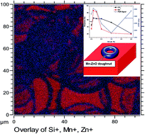
In this study, we report on the correlation between the magnetism and gas sensing properties of Mn-doped ZnO films grown via aerosol spray pyrolysis. The evolution of the structure, morphology, optical properties, and chemical state of ZnO with the Mn concentration was also investigated. ZnO doped with Mn (0.1 at%) demonstrated room-temperature ferromagnetism (RTFM) due to the uncompensated surface spins primarily originating from structural defects and oxygen vacancies (VO) on the surface, which act as active sites for the adsorption of oxygen species. The undoped ZnO structure revealed both FM and paramagnetism (PM) at the near surface of the film. Increased Mn doping destroyed the RTFM ordering due to improved PM features induced by Mn clusters on the ZnO surface and reduced amount of VO on the surface. However, ZnO films doped with Mn (0.1 at%) exhibited an improved sensing response to oxidizing gases compared to their counterparts, showing that films with RTFM with no PM contribution exhibit improved sensing properties. These analyses revealed that the nature of the film surface plays a substantial role in both their magnetic and sensing behaviors.
Additionally, among diluted magnetic semiconductors (DMS), Mn-doped ZnO was the most attractive because Mn has the highest possible magnetic moment at a valence state of 2+.17 However, local spin density approximation (LSDA) calculations suggested that Mn3+ may be more favored in the ground state of the system.18 Theoretical calculations predicted that Mn-doped ZnO exhibits ferromagnetism (FM) with a Curie temperature well above room temperature (RT).19–22 In DMS, the non-magnetic host ions are partially substituted by magnetic ions, which exploit the spin in magnetic materials along with the charge of electrons in semiconductors. Nonetheless, the origin of FM in TM-doped ZnO systems is not yet understood, and it is debated whether this is caused by defects other than the metal dopants. Recently, Straumal et al.23,24 analyzed a large number of experimental publications concerning the specific grain boundary area, which is the ratio of the grain boundary (GB) area to the grain volume, sGB. They observed that GBs are the key factor that determines the presence or absence of FM in ZnO. According to Straumal et al.,23 FM only appears if sGB surpasses a certain threshold value, sth.
However, both the gas sensing mechanism and the magnetization depend primarily on defects. It is well known that oxygen vacancies (VO) play a vital role in the gas sensing mechanism,25,26 and similarly, it is also understood that the presence of VO may lead to RTFM in MOS. Currently; there are only a few reports on the correlation between magnetism and sensing. Since VO is considered a common parameter for gas sensing and magnetism, in this work, we correlate the effect of magnetism on the sensing properties of the undoped and Mn-doped ZnO films towards oxidizing gases, such as NO and CO2. We show in detail that the nature of the magnetism greatly influences the gas sensing response of both undoped and Mn-doped films grown via aerosol spray pyrolysis. In addition, a correlation between the optical constants, crystal quality, and magnetism was also investigated using spectroscopic ellipsometry (SE). The origin of the defects responsible for mediating ferromagnetism and gas sensing properties in Mn-doped ZnO films was investigated using electron spin resonance (ESR), X-ray photo-electron spectroscopy (XPS) and photoluminescence (PL) spectroscopy. Additionally, the time-of-flight secondary ion mass spectrometry (TOF-SIMS) was also used to investigate the presence of Mn dopants and the homogeneity in the crystal lattice of ZnO in detail.
Films | 2θ(002) (°) | Crystallites size (nm) | Lattice strain, ε (×10−3) | a (Å) | c (Å) | V (Å3) |
---|---|---|---|---|---|---|
Undoped ZnO | 34.45 | 29.09 | 1.19 | 3.2489 | 5.2063 | 47.5904 |
0.1 at% Mn | 34.67 | 26.41 | 1.31 | 3.2501 | 5.1743 | 47.3329 |
0.5 at% Mn | 34.54 | 22.97 | 1.51 | 3.2549 | 5.1940 | 47.6535 |
2.0 at% Mn | 34.53 | 21.05 | 1.64 | 3.2729 | 5.1853 | 48.1013 |
Fig. 2 depicts the cross-sectional SEM analysis of the undoped and Mn-doped films. The cross-sectional view in Fig. 2a shows that columnar structures indeed grew perpendicular to the substrate with a parallel c-axis orientation. As shown in Fig. 2a, the shape of the columnar structures or grains appears to be elongated. The typical column size was estimated to be approximately 20–40 nm. It is important to note that, by doping the ZnO with 0.1 at% of Mn, the columnar structure was maintained and was visible across the film edge (Fig. 2b). At a higher doping level (0.5–2.0 at%), no columnar structure was observed.
![]() | ||
Fig. 2 Cross-sectional SEM micrographs of (a) undoped ZnO, (b) 0.1 at%, (c) 0.5 at%, and (d) 2 at% Mn-doped ZnO films. |
The crystal structure and orientation of the as-deposited and Mn-doped ZnO films grown for 30 min were investigated using XRD, and the results are shown in Fig. 3. These XRD patterns indicate that the films are polycrystalline in nature with a hexagonal wurtzite structure. The positions were indexed to the (100), (002), (101), and (102) planes, and the peak positions were determine to be consistent with the JCPDS [card 36-1451] of ZnO. No traces of manganese oxides or any binary zinc manganese phase were observed in any of the samples up to 2.0 at% Mn doping. This result clearly indicates that the speculated substitution of Zn2+ ions by Mn2+ ions did not alter the inherent Wurtzite structure of ZnO. A slight shift in the lattice constant of doped ZnO films was observed compared to undoped ZnO film, as shown in Table 1. This result is due to the larger ionic radius (0.83 Å) of the Mn2+ ions that replaced the smaller Zn2+ ions, which have a smaller ionic radius (0.74 Å). The shifting of the peak to a lower angle indicates substitution of larger Mn2+ in the Zn2+ site. As the Mn content increased, the diffraction intensity from the ZnO (002) peaks decreased, which indicates that the film crystallinity deteriorated with Mn incorporation and this in agreement with the SEM results. As shown in Fig. 3, small peak broadening also occurred with an increase in the Mn content. This small degree of broadening is the result of increasing strain (see Table 1) in the film due to Mn incorporation in the Zn lattice site29 and a corresponding increase in the volume of the unit cell with an increase in the Mn doping level. The average crystallite size of the Mn-doped ZnO films was determined using the Scherrer equation,30 and the lattice strain (ε) was calculated using the following relation:
![]() | (1) |
The typical XPS wide survey spectra of undoped and Mn-doped ZnO films showed that the as-prepared materials are pure without any impurities, showing only three main elements (i.e., O, Zn, and Mn, see ESI, Fig. S1†). High-resolution XPS analyses of Zn 2p were carried out to investigate how the electronic structure of Zn changes upon Mn doping of the Zn site. The Zn 2p3/2 XPS spectra of undoped and Mn-doped ZnO films are shown in Fig. 4. Based on the results presented in Fig. 4a, the undoped ZnO exhibited two symmetric peaks located at 1022.14 and 1047.61 eV. However, upon doping with Mn, the ZnO symmetric peaks shifted to 1021.8 and 1045.24 eV after fitting with a Gaussian, which is attributed to the partial substitution of Zn in the ZnO lattice by Mn2+ ions in the Zn–Mn bonding structure.31 Parts (d) and (e) of Fig. 4 indicate that the oxygen 1s (O 1s) spectra were asymmetric, indicating that multi-component oxygen species cannot be ruled out in the near-surface region of all these films. The peaks of the spectra fitted by two Gaussians were located at approximately 531.78 and 532.72 eV. The high-energy peak centered at approximately 532.72 was due to either the chemisorbed oxygen of the surface in the form of –OH, –CO3, absorbed H2O, or absorbed O2 or primarily due to surface contamination. The medium binding energy component centered at approximately 531.78 eV (Ob) corresponded to O2− ions in the oxygen deficient regions within the ZnO matrix and/or Zn–OH groups.32 Therefore, the changes in the intensity of the Ob relative area may be related to the concentration of oxygen vacancies (VO). Based on the results in Fig. 4 and Table 2, the Ob peak was present in all of the samples and substantially decreased with Mn dopants up to 2.0 at%.
![]() | ||
Fig. 4 XPS deconvoluted spectra of (a–c) Zn 2p3/2, and (d −e) O 1s core level of the undoped and Mn-doped ZnO films. |
Films | Oa position (eV) | Ob position (eV) | Relative intensity of Oa (%) | Relative intensity of Ob (%) |
---|---|---|---|---|
Undoped ZnO | 532.72 | 531.47 | 79.35 | 21.65 |
(0.1 at%) Mn–ZnO | 532.40 | 531.18 | 63.13 | 36.87 |
(2.0 at%) Mn–ZnO | 532.27 | 531.15 | 94.47 | 5.53 |
The valence band of Mn was investigated by measuring the Mn 2p XPS spectra shown in Fig. 5. These two weak XPS peaks at binding energies of 641.7 eV and 657.8 eV correspond to Mn 2p3/2 and Mn 2p1/2, respectively. The peak centered at approximately 641.7 eV was due to the presence of Mn in its Mn2+ oxidation state, which is in good agreement with the value reported in the literature.33 Therefore, these results indicate that the Mn dopant ions were indeed in the divalent state, which is evident that Mn as a dopant substitutes for part of Zn in the ZnO lattice.34 This result implies that, with the addition of Mn2+ ions, the bond configuration and lattice structure in the ZnO crystal lattice deteriorated, which is consistent with the XRD results shown in Fig. 3. Therefore, at higher doping levels (2.0 at% Mn), the intensity of the Mn2+ peak decreased probably because of segregation, and a satellite peak appeared at approximately 663.10 eV.
![]() | ||
Fig. 5 Deconvoluted core level XPS spectra of Mn 2p of the (a) 0.1 at% and (b) 2.0 at% Mn-doped ZnO films. |
To investigate the presence of Mn dopants and their homogeneity distribution in the crystal lattice of ZnO, TOF-SIMS chemical imaging analyses were performed, as shown in Fig. 6. Only elements of interest (e.g., Zn and Mn) are shown. Parts (a) to (d) of Fig. 6 show the positive ion mapping of pure ZnO film during depth profiling after 67 scans while Fig. 6d is the overlay of Si+, Zn+, and 66Zn+, wherein each particle is clearly observed. The Si+ signal arose from the Corning glass substrate. The micrographs depict the Zn+ and 66Zn+ elemental or chemical distribution across the surface. The results also confirm the formation of “spaghetti-like” or nanograins structures as observed by SEM. The 0.1 at% Mn-doped sample in Fig. 6e and f also showed the Mn+ signal, confirming that Mn was homogeneously incorporated in the ZnO surface. Fig. 6g shows that the Mn was evenly distributed across the surface within an area of 100 μm × 100 μm, although the signal was weak for the lower doping concentration. In addition, the “doughnut-like” structures were also visible, as previously observed in SEM results. The 0.5 at% Mn-doped sample also confirmed the homogenous distribution of Mn in the ZnO matrix. The overlay image shows that, the Mn ions were visible at 0.5 at% doping level. At a higher doping level (1.0 at%, parts (m) to (p) of Fig. 6), the Mn+ ions were not uniformly distributed; they were mostly observed on the “doughnut-like” structures surface, which are more visible in the 3D images shown in the ESI (Fig. S2†). The arrows on the overlay image, Fig. 6m, indicate the uncovered Corning substrate.
![]() | ||
Fig. 6 TOF-SIMS images of (a–d) pure ZnO, (e–h) 0.1 at% Mn–ZnO, (i–l) 0.5 at% Mn–ZnO, (m–p) 1.0 at% Mn–ZnO. |
The absorption coefficient (α) of the Mn-doped ZnO films with different compositions was calculated from the obtained k values using the following relation:
![]() | (2) |
(αhν)2 = A(hν − Eg) | (3) |
Films | Thickness (nm) | Roughness (nm) | Carrier concentration (cm−3) | Mobility (cm2 V−1 s−1) | E*g (eV) | E**g (eV) |
---|---|---|---|---|---|---|
a E*g was estimated from spectroscopic ellipsometer measurements. E**g was estimated from UV-Vis measurements. | ||||||
Undoped ZnO | 173.01 | 11.63 | 5.10 × 10¹⁶ | 6.58 | 3.23 | 3.24 |
(0.1 at%) Mn | 97.60 | 3.99 | 2.91 × 10¹⁷ | 48.16 | 3.14 | 3.23 |
(0.25 at%) Mn | 96.51 | 3.68 | 4.90 × 10¹⁵ | 1.79 | 3.12 | 3.22 |
(0.5 at%) Mn | 90.92 | 2.61 | 3.71 × 10¹⁵ | 1.15 | 3.22 | 3.18 |
(2.0 at%) Mn | 90.70 | 2.42 | 4.40 × 10¹⁴ | 0.12 | 3.11 | 3.21 |
The electrical properties of the undoped and Mn doped ZnO films with different Mn concentrations measured using Hall effect system are listed in Table 3. As listed in Table 3, the undoped shows a carrier concentration of 5.10 × 1016 cm3. However, upon doping with 0.1 at% Mn, a slight increase in carrier concentration is observed. As the Mn doping increases, the carrier concentration and mobility decrease. At lower concentration (0.1 at% Mn), oxygen vacancies increase (see Fig. 8a, PL analyses), which results to an increase in carrier concentration. The oxygen vacancies, as a shallow n-type dopant play an important role in ZnO conductivity.38 Since, the mobility of the charge carriers depends on the scattering mechanisms in the film; therefore, the decrease in electron mobility in Table 3 is probably due to the increased impurity scattering centers by doping more Mn.39
To investigate the presence of defects in Mn–ZnO films, PL measurements were performed as shown in Fig. 8a. The undoped ZnO film exhibited a broad emission peak at approximately 380–550 nm. The absence of the sharp near band edge (NBE) at 385–390 nm may be due to higher defects possessed by these structures. In general, the reported defects present in ZnO-based nanostructures are oxygen vacancies with different charged states, Zn vacancies, Zn interstitials, and adsorbed molecules.40,41 Previous studies indicated that the resulting defect-related emissions for these defects typically occur near the blue-green (approximately 480–550 nm), yellow (approximately 550–610 nm), and orange-red (approximately 610–750 nm) regions.41 Therefore, to obtain a detailed understanding of the effect of individual defects on the magnetic properties of the ZnO nanostructures, a three-peak (Gaussian) fitting method of the broad visible emission was adopted. The de-convoluted spectra of the undoped ZnO in Fig. 8b exhibit three peaks at approximately 390, 441, and 511 nm. Therefore, the UV emission at approximately 390 nm was due to exciton recombination through an exciton–exciton collision process. The emission peak at 441 nm may be due to an electron transition from the Zn interstitial energy level to the valence band.42 In addition, the green PL emission band at 511 nm may be assigned to oxygen vacancies (VO) in ZnO. This luminescence may be due to the recombination of photogenerated holes with singly ionized oxygen vacancies .42,43 Based on the results from parts (a) to (d) of Fig. 8, the intensity of the emission band related to
was higher for the 0.1 at% doped material than its counterparts, which indicates that the 0.1 at% doped material contained more
. The 588 nm emission band is typically attributed to the 4T1(4G) → 6A1(6S) transition within the 3d shell of the Mn2+ ion.44 Here, the 4T1(4G) → 6A1(6S) emission intensity increased and reached a maximum at a Mn2+ concentration of 0.5 at% (Fig. 8b). In addition, the observed sharp decrease in intensity of the Mn2+ emission for ZnO films doped at a concentration above 0.5 at% Mn may be attributed to the concentration quenching effect due to the pairing or coagulation of the Mn ions, which is consistent with the XPS and TOF-SIMS results (Fig. 5a and 6).
To further confirm the presence of defects, EPR analyses of the Mn–ZnO films were carried out at room temperature and the results are shown in Fig. 9. The spectrum in Fig. 9a exhibits two absorption peaks associated with paramagnetism (PM) and ferromagnetic resonant (FMR) fields at 150 and 320 mT, respectively. The ESR results indicate that all the films possessed PM features at 150 mT except for the 0.1 at% Mn-doped material. However, at higher magnetic fields (>320 mT), a FM signal was observed for both the undoped and Mn-doped films up to 1.0 at%, which is consistent with the magnetization measurements shown in the ESI (Fig. S8†). This feature decreased as the PM features (see inset, Fig. 9b) increased with Mn concentration. Mn-related oxides, such as MnO, MnO2, and Mn2O3, are known to be antiferromagnetic while Mn3O4 is ferromagnetic below 45 K.45 Therefore, the observed room temperature (RT) FM in the current work excludes the presence of the above-mentioned oxides, and the RTFM is only attributed only to the incorporation of Mn2+ ions into the ZnO host lattice and the high VO content, as depicted in the PL analyses (Fig. 8), which is in good agreement with our previous results.42 Furthermore, Straumal et al.23,24 have shown that the topology of a grain boundary network in the material and the shape of the grain boundaries have a significant effect on FM. They found that saturation magnetization changed drastically with the topology of the grain boundary network in Mn-doped ZnO. Therefore, the observed FM for undoped and 0.1 at% Mn-doped ZnO film may also be due to the shape of nanograins, which appeared to be elongated according to SEM. Additionally, the lower FMR signal observed for the undoped sample compared to 0.1 at% may be due to larger nanograins (coarser grain). Tietze et al.46 have reported that a film with an average grain size of 31 nm (i.e. finer grains) has larger magnetization compared to the film with an average grain size of 65 nm (coarser grains) because the value of sGB was 5.32 × 10⁷ m−1 for the fine-grain sample, while the value of sGB was 2.65 × 10⁷ m−1 for the coarser-grain sample. Additionally, Kumar et al.47 observed FM on Fe (0.06)-doped ZnO showing a sGB value of 41 × 106 m−2 m−3. Thus, for our system (0.1 at% Mn–ZnO), sGB value is well above the threshold value, viz. sGB = 6.24 × 10⁷ m−1. Moreover, the FM spectra for both the undoped and Mn-doped films showed sextet hyperfine structures, which are related to interactions between the electronic state and the nuclear spin angular momenta in Zn2+. A g-factor of about 1.9965–2.0013 is observed for all the samples, which was related to VO and VZn.7,42,43,48,49
![]() | ||
Fig. 9 ESR spectra of the undoped and Mn-doped ZnO films and (b) corresponding spectra of the inset in (a). |
At higher doping level (i.e., 2.0 at% Mn), a magnetic transition occurs, and a signal related to FM transforms to a sharper peak related to PM (see the circle, Fig. 9a). This indicates that the film is dominated by the same spins, which are randomly oriented clusters with some ferromagnetic features that are still present even at relatively high Mn concentration. The observed PM was most likely caused by tiny deposited Mn particles that tend to agglomerate among themselves on the surface of ZnO at higher doping levels and suppress the number VO (see XPS and PL analyses, Fig. 4 and 8), which reduces the FM nature of the sample. Wang et al.50 reported that Mn-doped ZnO films with a higher Mn content resulted in a shorter magnetic coupling distance between Mn atoms, which is energetically favorable for Mn2+ ions to obtain antiferromagnetism.
Fig. 10 illustrates the variations in the response of Mn-doped ZnO gas sensing films exposed to CO2 gas at room temperature. In stage A, the films are photo-reduced using a UV light. The increase in conductance (stage A) was due to the generation of free carriers within the film and photodesorption of surface species with a subsequent thinning of the electron depletion layer near the film surface. In stage B, when the UV lamp was turned off, the conductivity decreased due to a limited adsorption process on the film surface. In stage C, when the sensing films were exposed to the oxidizing gas (i.e., CO2) at room temperature, the conductance decreased further with a distinct exponential decay corresponding to the sensing gas concentration.
![]() | ||
Fig. 10 Current vs. time curve of the Mn–ZnO sensing film for various Mn concentrations towards CO2 at room temperature. |
Fig. 11 shows the reproducibility of the temporal response of Mn–ZnO sensing films exposed to CO2 at room temperature. The sensors maintained their initial response amplitude without a clear decrease up on four successive sensing tests to CO2, demonstrating that these sensors had good repeatability. This behavior was also observed for NO gas (results not shown). Therefore, all these observations specify that Mn–ZnO sensing films are good candidates for the development of high-performance CO2 sensors operating at room temperature.
![]() | ||
Fig. 11 Sensing performance and repeatability of Mn–ZnO sensing films with various Mn concentrations towards CO2 at room temperature over a long working period. |
Fig. 12a displays the gas sensing responses of the undoped and Mn-doped gas sensing films exposed to various oxidation gases at room temperature. Due to its intrinsic defects, the ZnO material showed an n-type conducting feature. Although Mn doping causes an increase in film conduction owing to the sp–d exchange interaction, the addition of Mn will not change the conduction type. Therefore, in the sensing process, the adsorption of oxidizing gases (i.e., CO2 or NO) on the surface will increase the resistance of the film. In this study, the gas sensing performances were characterized in terms of the gas-sensing response (S), which is defined as:
![]() | (4) |
This result indicates that a higher concentration of Mn doping in ZnO decreases rather than increases number of reactive sites. Based on the results in Fig. 12a, we infer that the 0.1 at% Mn-doped ZnO film, which showed a higher FM signal, was more sensitive to oxidation gases than its counterparts. Therefore, the gas sensing and magnetic studies imply that Mn may form clusters on the ZnO surface and reduce the FM nature (due to contribution from PM) of the sample, and this result was observed in XPS and PL analyses where the amount of VO decreased upon increasing the Mn concentration as dopants on the ZnO surface increased. Therefore, this is the reason for the reduced response of ZnO containing higher level of Mn dopants (0.25–2.0 at%). Additionally, the sensor response to NO gas was obviously superior to the response to CO2 gas at lower doping concentrations (0.1 at% Mn). Based on these results, we conclude that, the selectivity of the Mn–ZnO gas sensing films toward NO gas is excellent at lower Mn doping levels.
Fig. 12b demonstrates the response magnitude versus the concentration of NO gas in the range of 10–100 ppm under UV-light. Fig. 12b shows that the 0.1 at% Mn sensing film had a great response to NO gas compared to the 0.25 at% and 2.0 at% Mn-doped ZnO films (results not shown). Its response increased rapidly with the NO gas concentration. The fabricated sensor exhibited a clear response of approximately 58.6 even for a very low NO gas concentration of 10 ppm. Additionally, at 100 ppm NO, the highest response of approximately 86% was observed without any saturation trend. As depicted in the figure, the sensor had a clear linear dependence curve in the range of 10 to 100 ppm NO gas, which confirms that the as-fabricated gas sensor can be considered a possible candidate for NO detection. Fig. 12c depicts the sensor response versus time for the 0.1 at% Mn exposed to various concentrations of NO gas. As confirmed in Fig. 12c, the sensor response increases with an increase in gas concentration. Additionally, the sensing films were also tested to H2 gas, however, only 0.1 at% showed a response to H2 (see ESI, Fig. S11†), disclosing poor response and recovery over a long period compared to CO2 and NO gases. Nonetheless, previous studies have reported a higher sensing response to H2 and ethanol gases using ZnO nanostructures.52–55 Moreover, Rout et al.54 have shown that the relative humidity plays an important role on the gas sensing. They observed that, at higher relative humidity concentration, the sensing response decreases.
The slope of the curves in Fig. 12b was used to study the sensitivity.56 Fig. 12b shows that the response of the 0.1 at% Mn-doped film tested with NO increased linearly resulting in a sensitivity of 0.34 ppm−1 in the range of 20–80 ppm. The 0.25 at% and 2.0 at% Mn-doped films showed a linear trend at 10–50 ppm and started to saturate at higher concentrations. At 10–50 ppm, these films had a sensitivity of 0.19 ppm−1 and 0.06 ppm−1 respectively. Therefore, these findings show that the 0.1 at% Mn-doped sensing film had a higher sensitivity to NO gas compared to other sensing films. This indicator is very vital for gas sensing, since it indicates how accurately the sensor can differentiate one analyte concentration from another one.
Table 4 shows a comparison of the sensing films on NO and CO2 gases prepared in this study and those published in the literature. As shown in Table 4, the 0.1 at% Mn-doped ZnO sensing films prepared in this work had either comparable or higher responses when compared to ZnO materials prepared using different methods and tested at different operating temperatures and gas concentrations.
Sensing element | Method | Gas concentration (ppm) | Operating temperature (°C) | Response | Ref. |
---|---|---|---|---|---|
Ca doped ZnO | Sol–gel | 2500 ppm CO2 | 450 | 117 | 57 |
50% La-loaded ZnO | Hydrothermal method | 5000 ppm CO2 | 400 | 65% | 58 |
ZnO nanowires | Chemical vapour deposition | NO 10 ppm | Under UV-light | 46% | 59 |
ZnO–In2O3 composites | Co-precipitation (powder) | 19 ppm NO | 200 | 60 | 60 |
10 ppm NO | 150 | 65 | |||
ZnO thin film | DC reactive magnetron sputtering | 1000 pm CO2 | 300 | 90% | 61 |
0.1 at% Mn–ZnO nanorods | Spray pyrolysis | 100 ppm NO | Under UV-light | 87% | This work |
100 ppm CO2 | 66% |
The UV-activated room-temperature gas sensing mechanism is demonstrated in Scheme 1. It is well known that the gas-sensing mechanism of undoped and Mn–ZnO-based sensors involves surface-controlled processes. According to these processes, the resistance change is governed by the types of molecules and amount of oxygen species adsorbed on the surface. Once the Mn–ZnO-sensing films are positioned in ambient air (or in the dark), atmospheric oxygen molecules adsorb onto the surface or grain boundary sites, where they become ionized by accepting electrons from the conduction band to form O− and O2− ions at the grain boundaries and creates a space charge at the grain boundary, as depicted in the reactions below and Scheme 1a.62 These are the characteristics of n-type metal oxides, such as ZnO. The adsorption of oxygen ions is the most imperative process in sensors since these ions are the most reactive surface species that make the material sensitive to the presence of oxidizing gases.
O2(g) → O2(ads) | (5) |
O2(ads) + e− → O2−(ads) | (6) |
O2−(ads) + e− → 2O−(ads) | (7) |
O−(ads) + e− → O2−(ads) | (8) |
A depletion layer forms in the surface region of the Mn-doped ZnO films due to the consumption of electrons in the surface region of the films, which results in a decrease in electrical resistance. When the Mn-doped ZnO film is exposed to UV light with photon energy larger than the energy band gap of ZnO, electron–hole pairs generated. Upon reaching the surface of the films, some of the photo-generated electrons and holes recombine. As a result, most of the photo-generated holes react with the adsorbed oxygen ions on the surface, as shown in the following reactions and Scheme 1b:63
h+(hν) + O2−(ads) → O2(g), | (9) |
![]() | (10) |
![]() | (11) |
Consequently, the surface depletion layer width is reduced, and oxygen species are photo-desorbed from the surface (Scheme 1c). However, the photo-generated electrons also contribute to a decrease in the depletion layer width and in the resistance of the gas sensing films.
Since NO behaves as an oxidizing gas on Mn-doped ZnO films, the resistance of n-type ZnO films increases as the NO gas chemisorbs on the surface. The increase in the resistance of the ZnO sensing film may be due to NO adsorption in the charged form (NOads−) or to the reduction of NO to form N2O, as described by the following reactions and Scheme 1d and e:64–67
NO + e → NOads− | (12) |
2NO + e → N2O + Oads− | (13) |
When the sensing films are exposed to CO2, which is also an oxidizing gas, the following reactions occur (see Scheme 1d and e):68,69
CO2(gas) + e− → CO2−(ads) | (14) |
CO2−(ads) + O−(ads) + 2e− → CO(gas) + 2O2−(ads) | (15) |
The adsorption of O− is a very interesting step in metal-oxide gas sensors, because the O− ions assist the adsorbed oxidizing ions in transporting the electrons from the metal oxide surface. The concentration of electrons on the surface of the metal oxide decreases and the resistance of the n-type metal oxide layer increases accordingly. In contrast, the resistance of a p-type metal oxide surface decreases because the extracted electrons result in the generation of holes in the valence band.
Footnote |
† Electronic supplementary information (ESI) available: Additional results related to TOF-SIMS showing the 3D images and magnetization results on undoped and Mn doped ZnO films. See DOI: 10.1039/c5ra27154a |
This journal is © The Royal Society of Chemistry 2016 |