Localized surface plasmon resonance on Au nanoparticles: tuning and exploitation for performance enhancement in ultrathin photovoltaics

Vivek Garga, Brajendra S. Sengara, Vishnu Awasthia, Aaryashreea, Pankaj Sharmaa, C. Mukherjeeb, Shailendra Kumarc and Shaibal Mukherjee*a
aHybrid Nanodevice Research Group (HNRG), Electrical Engineering, Indian Institute of Technology, Indore 452020, India. E-mail: shaibal@iiti.ac.in; Fax: +91-731-2361482; Tel: +91-731-2438961
bMechanical and Optical Support Section, Raja Ramanna Centre for Advanced Technology (RRCAT), Indore-452013, India
cIndus Synchrotron Utilization Division, Raja Ramanna Centre for Advanced Technology (RRCAT), Indore-452013, India

Received 1st December 2015 , Accepted 28th February 2016

First published on 1st March 2016


Abstract

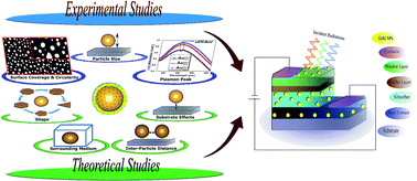
We report a detailed correlation analysis of the size, shape, and distribution of Au nanoparticles (NPs) on fine-tuning of localized surface plasmon resonance and optical absorption cross-section. Experimental analysis of annealing temperature and initial Au layer thickness on NP parameters such as size, interparticle distance, surface coverage, and circularity factor has been studied. The effect of annealing on the morphological, structural, dielectric, and elemental behavior of Au NPs has been reported. Theoretically, we have analyzed the tuning of LSPR and absorption cross-section peaks by varying NP parameters, surrounding medium, and substrate. This report is critical in terms of predicting performance enhancement of ultrathin photovoltaics with varied cell architectures.


A. Introduction

Plasmonic nanoparticles (NPs) are appreciable for scientific research because of their interesting applications in the field of photonics, electronics, optical sensing, imaging, and drug delivery.1–4 Most of these interesting applications are built upon the captivating surface plasmon resonance (SPR) feature of the nanoparticles. SPR arises in metal NPs, with dimensions smaller than that of the incident wavelength (λ), as a collective charge density oscillation, when subjected to an electric field associated with the incident field,5 which is a function of size, shape, interparticle distance, surface coverage, and surrounding medium.6–11 Plasmonic NPs are emerging as a possible solution to enhance the efficiency of mainly thin film solar cells (SCs).12–16 The NPs compensate high losses in SCs, occurring due to partial absorption of the solar spectrum and thermalization losses of photons. These losses are the primary challenges that have generally been addressed to overcome the limitations of photovoltaic efficiency. The incorporation of NPs enhances the light scattering in the photoactive absorber layer, which improves the overall performance of SCs. If scattering efficiencies of NPs is less than 50%, it may lead to heat dissipation and absorption suppression.5,17 This results into undesired reduction of photocurrent in SCs.13 Moreover, the change in the parameters (such as size, shape, inter-particle distance, surface coverage, and surrounding medium) of NPs affects their polarizability. In general, this phenomena causes a red shift in the resonance wavelength and leads to enhancement in the absorption of photons having less energy in comparison to band gap energy of the absorber.19 Enhancement in the photo-absorption below band gap edge in thin film SCs produces optically thick, but physically thin photovoltaic absorbers, and could motivate ultrathin and high efficiency photovoltaic design.12,15,16,20

Absorption and scattering of incident photons rely on the NP polarizability, which can be tuned by NP parameters as demonstrated elsewhere.1,5,9,21–23 However, till date there has not been a report consisting of extensive experimental and analytical studies incorporating correlation of generation and variation of localized surface plasmon resonance (LSPR) effect of Au NPs and optical scattering cross-section. In this article, a detailed theoretical and experimental analysis of the effect of Au NPs parameters on LSPR has been performed. For SC applications, Au NPs are generally used because of their absorption falls in the (∼2.3 eV) visible range and it is less reactive in environmental conditions.24 In general, Au NPs are grown by colloid chemical synthesis, electrodeposition method, laser ablation, and vacuum deposition technique.1 The control in terms of the distribution of NPs is achieved from mask templates in colloid chemical synthesis and electrodeposition,25 light manipulation in laser ablation,26 and implantation with focused ion-beam lithography in combined chemical and vacuum deposition techniques.8 However, all these techniques require complex and expensive procedure, which limits the direct incorporation of NPs into the required layers of SCs. We report a simple and cost-effective process of sputtering deposition followed by post-deposition annealing to generate and suitably engineer the distribution, size, and shape of Au NPs. Thermal annealing is particularly well suited for photovoltaic application as it can be implemented using large area and high throughput process and utilizes equipment that is already a part of conventional solar cell fabrication process. Hereby, adopting this methodology, Au plasmonic layers can easily be integrated along surface of the SCs,15 embedded inside photo-active absorber layer,15 or integrated into back contact layer.15,27 For theoretical studies, simulation is performed using a MNPBEM toolbox of MATLAB by utilizing the Boundary Element Method (BEM) computational scheme.24,28 Simulated data shows proper agreement to the experimentally obtained data.

B. Experimental

Ultrathin layers of Au films with thickness of 5 and 10 nm are grown on low resistive single crystal p-type Si (100) wafers using pulsed DC sputtering system (Advanced Energy Inc., USA) at deposition rate of 0.9 A s−1, having chamber base pressure of 1.4 × 10⁻⁷ mbar and deposition pressure of 4 × 10⁻³ mbar. The thickness of deposited Au films is further confirmed by spectroscopic ellipsometry measurement. Au films on Si substrates are annealed at 500, 600 and 700 °C (Au500 °C5 nm, Au600 °C5 nm, Au700 °C5 nm and Au500 °C10 nm, Au600 °C10 nm, Au700 °C10 nm) in Nabertherm GmBh annealing furnace. The annealing process is carried out in three steps: (1) temperature enhancement is performed with a ramp up rate of 6 °C per minute, (2) annealing at desired temperature for 2 hours, and (3) natural cooling of the samples up to the room temperature.

Crystalline quality of Au samples is analyzed using Rigaku SmartLab system with Cu Kα radiation (0.154 nm). For studying the morphological properties of samples, field-emission scanning electron microscope (FESEM) based on Supra55 Zeiss lens is used. Elemental properties of the samples are examined by X-ray photoelectron spectroscopy (XPS) utilizing PHOIBOS 100 analyzer with an Al Kα radiation (1486.6 eV) as an excitation source. Optical properties, such as dielectric functions, dispersion curves, and absorption, of the samples are analyzed by using M-2000D J. A. Woollam spectroscopic ellipsometry (SE).

C. Results and discussion

Morphological characterization

Fig. 1(a)–(f) illustrate the FESEM images of annealed Au samples with a thickness of 5 and 10 nm, respectively. The formation of both NPs and their clusters is observed after annealing process and the distribution of NPs on the substrate surface is non-uniform. It is well-known that these NPs are formed due to surface tension and compressive stress associated with the mismatch of the thermal expansion coefficients of Si and Au.29 In order to extract crucial parameters such as the particle size, inter-particle distance, surface coverage, and circularity factor of Au NPs processing of FESEM images are performed by ImageJ software.30
image file: c5ra25575a-f1.tif
Fig. 1 (a)–(f): FESEM images of 10 and 5 nm samples annealed at different temperatures. Insets show magnified images and the histograms of NP count vs. particle size, as in (a), (c) & (e). (g) Variation of particle size and circularity factor with annealing temperature, (h) variation of inter-particle distance and surface coverage with annealing temperature for 5 nm thick Au sample.

Results of processing (refer Table 1) of FESEM images are plotted in Fig. 1(g) and (h). From the results of image processing for 5 nm thick Au sample, it can be inferred that the mean Au NP size increases from 42.84 to 52.72 nm and the average inter-particle distance decreases from 69.67 to 60.97 nm with the corresponding increase in annealing temperature (Ta). The reduction in the average inter-particle distance leads to an enhancement of the inter-particle coupling effects and surface coverage area.5,22,31 As observed in Table 1, for 5 nm film the surface coverage area increases from 17.58 to 31.14% and the average circularity factor of the NPs decreases from 0.94 to 0.76 as Ta is increased from 500 to 700 °C. Similar variations of NP parameters are observed for 10 nm-thick Au samples annealed at 500 and 700 °C (Au500 °C10 nm and Au700 °C10 nm), as shown in Fig. 1(b) and (f). However, Au samples annealed at 600 °C (Au600 °C10 nm) exhibits a different trend, as could be observed in Fig. 1(d). It might be due to more interlinks between the NPs, which gradually lead to the formation of larger NP clusters as shown in Fig. 1(d). For sample Au600 °C10 nm, formation of NPs clusters and smallest surface coverage of ∼7.99% are observed. These parameters of Au600 °C10 nm sample differs from those from the other annealed Au samples and because of this reason Au600 °C10 nm sample shows anomalous behavior during other experimental characterizations, as explained later in this article. However, on an overall basis the inference that we can draw from the morphological characterizations is that with the increase in Ta, the values of NP size and surface coverage increases while inter-particle distance and average circularity factor decreases.

Table 1 Results from image processing of FESEM data
Sample Average particle size (±5 nm) in nm Surface coverage (in %) Average interparticle distance (±5 nm) in nm Circularity factor
Au700 °C5 nm 52.71 31.14 60.97 0.76
Au600 °C5 nm 50.46 25.77 65.81 0.88
Au500 °C5 nm 42.84 17.58 69.67 0.94
Au700 °C10 nm 101 22.48 134.83 0.86
Au500 °C10 nm 77 18.16 143.23 0.95


Structural characterization

XRD patterns of annealed Au samples are plotted in Fig. 2. Bragg reflection peaks at 2θ = 38.2°, 44.3°, 56°, and 61.7° corresponding to Au (111), Au (200), Au5Si2 (308), and Au (220) crystal planes, respectively are observed. Additionally, XRD peaks at 2θ angles of ∼69.2° and ∼69.45° corresponding to Si (100) and Au5Si2 (416), respectively are shown in the insets of Fig. 2. For Au700 °C5 nm sample, diffraction peaks corresponding to (111) and (220) planes are observed. In this case, the intensity of (220) is four-fold higher than that of (111) and thus almost 80% of crystals formed are in (220) plane for Au700 °C5 nm sample. For Au600 °C5 nm sample, three diffraction peaks corresponding to (111), (200), and (220) planes are observed and in this case ∼70% of the crystals are oriented in (220) plane, ∼22% crystals are in (111) orientation, while remaining ∼8% of the crystals are in (200) orientation. For Au500 °C5 nm sample, two prominent diffraction peaks corresponding to (111) and (200) planes are observed and in this sample ∼55% of crystals are in (111) plane while remaining ∼45% are in (200) plane.
image file: c5ra25575a-f2.tif
Fig. 2 (a) and (b): XRD spectra of 5 nm and 10 nm annealed samples. Insets show magnified XRD peaks of Au silicide and Si.

As observed in Fig. 2(b), it can be inferred that for sample Au700 °C10 nm, diffraction peaks associated with Au (111) and Au (220) planes are observed. In this case, 55% of the Au crystals planes are (111) oriented and remaining 45% are in (220) orientation. In case of Au600 °C10 nm sample, two diffraction peaks corresponding to (111) and (200) atomic reflections are present. Here, ∼66% crystals are in (111) orientation and rest ∼33% are in (200) orientation. For Au sample annealed at 500 °C, two diffraction peaks corresponding to (111) and (200) are present, in which ∼90% of the crystals are in (111) orientation and remaining 10% are in (200) orientation. Formation of Au5Si2 oriented in (416) plane is observed for all the annealed Au samples. Moreover, formation of Au silicide becomes more prominent with the corresponding increase in the Ta for both 5 and 10 nm-annealed Au samples. Additionally, peak associated with Au5Si2 oriented in (308) is also observed for 5 nm samples annealed at 600 and 700 °C, while for 10 nm sample it is observed only for sample annealed at 700 °C. From Fig. 2 it can also be observed that with the decrease in Ta the probability of formation of (111) crystal planes increases. From FESEM images as in Fig. 1 it is observed that more number of circular NPs are formed at reduced Ta.32 Thus, it can be inferred that formation of (111) crystal planes is correlated with the circular nature of NPs. Moreover, a closer examination reveals that the Bragg angle corresponding to (111) crystal plane shifts to slightly larger value as the value of Ta reduces. This phenomenon indicates a lattice contraction in Au NPs.33,34

Elemental characterization

To determine the elemental properties of Au NPs, XPS measurement has been performed. Fig. 3(a) and (b) illustrate XPS spectra of all 5 and 10 nm annealed Au samples. In XPS spectra, major peaks corresponding to Au 4f7/2 (∼84 eV), Au 4f5/2 (∼87.71 eV), Si 2p (∼99 eV), SiO2 (∼103 eV), C 1s (∼286 eV), Au 4d5 (334 eV), Au 4d3 (353 eV), Au 4p3/2 (∼531 eV), Au 4s (∼762) and O (auger) (980 eV) are clearly observed. From the insets of the Fig. 3(a) and (b) it is evident that the core level peaks of 4f7/2 and 4f5/2 of Au are shifted towards higher values of binding energy (BE) in comparison to the bulk phase values (Au 4f7/2 = 84 eV and Au 4f5/2 = 87.7 eV) for most of the annealed Au samples such as Au500 °C5 nm, Au600 °C5 nm, Au500 °C10 nm and Au700 °C10 nm, which could be due to a reduced final state screening attributable to reduced metallic conductivity35 and also be an indicator of silicide formation.36 The shift towards higher values of BE for Au core level peaks of 4f7/2 and 4f5/2 increases with the corresponding reduction in the average dimension of NPs, as observed in Table 1. Similar experimental observations are reported by Sham et al.37 and Peters et al.38
image file: c5ra25575a-f3.tif
Fig. 3 XPS spectra of (a) 5 nm and (b) 10 nm annealed Au samples. Insets show magnified version of XPS peaks for Au 4f, Si and SiO2.

However, for sample Au700 °C5 nm and Au600 °C10 nm, the shift of Au core level peaks of 4f7/2 and 4f5/2 is observed towards lower values of BE as compared to those of corresponding bulk core level peaks. It can be explained by initial state effects due to 6s to 5d charge reorganization for less coordinated surface atoms.39 Such interatomic charge transition causes a large final state screening, which is due to contraction in the 5d shell, resulting in smaller BE for less coordinated Au atoms in comparison to the fully coordinated bulk atoms.38 Distinct spectral changes are observed for Si 2p and SiO2 XPS peaks with the increase in Ta. As Ta increases from 500 to 700 °C, a small shift to lower values of BE for the Si 2p peaks is observed, along with the peak of SiO2 and the splitting between peaks of Si 2p and SiO2 peaks is ∼4.6 eV, nearly 0.8 eV higher than the typical reported value of 3.8 eV.36 This can be attributed to the formation of gold silicide.36,40 It can be observed from Fig. 3, as the average size of NP decreases, intensity of Au 4f7/2 and 4f5/2 XPS peaks decreases and full-width half-maximum (FWHM) values of those XPS peaks increases. The loss in the observed XPS intensity can be attributed to the occurrence of the localized surface plasmon resonance (LSPR) in Au NPs.33 The broadening of XPS peaks with declining NP size can be attributed to both the increasing inhomogeneity of Au atoms in smaller clusters (increasing surface/bulk ratio) and the presence of more localized unoccupied d states at the Fermi level, enhancing a many-body effect known as Doniach-Sunjic line shape.33,41,42

Spectroscopic ellipsometry measurement

SE is a non-destructive, sensitive and powerful analytical technique to study the optical response of various materials. In ellipsometric measurements, change in the polarization state of the reflected light from the surface of the film is given in terms of ellipsometric angles [psi (Ψ) and delta (Δ)]. By fitting, the measured values of Ψ and Δ using appropriate model enables precise extraction of the optical constants and accurate thickness. Ellipsometric measurements of annealed samples along with 5 nm (AuWA5 nm) and 100 nm (AuWA100 nm) unannealed Au samples are performed. All ellipsometric measurements are performed with an incidence angle of 70° in the wavelength range of 350–1000 nm. The measured data is fitted by B-spline model43–45 using CompleteEASE software46 and the model shows good agreement with the experimentally obtained data in the entire spectral range.
Ellipsometric angles. Ψ spectra for annealed 5 and 10 nm samples are depicted in Fig. 4(a) and (b), respectively. In the observed spectra, peaks are observed in the visible region at ∼550 nm corresponding to LSPR peak. This LSPR peak shows red shift and broadening with the increase in Ta. In fact, as Ta increases, the average size of Au NPs also increases (as in Table 1), which leads to a gradual reduction in the concentration of free electrons in NPs. This, in turn, weakens the plasmonic field of the corresponding LSPR peak causing the peak to broaden and red shifted.11 This phenomenon is observed for 5 nm annealed Au samples and for Au500 °C10 nm and Au700 °C10 nm samples. However, for Au600 °C10 nm sample, blue shift in LSPR peak position is recorded, when compared other 10 nm samples. From Fig. 4(a) and (b), it is obvious that that the LSPR peak for 5 nm annealed Au films are more prominent than that for 10 nm annealed Au films; and this indicates a comparatively better LSPR generation in 5 nm Au films. Additionally, it is also observed that Ψ(λ) spectra display continuous decline for 5 nm un-annealed Au sample (AuWA5 nm) and constant rise for 100 nm un-annealed Au sample (AuWA100 nm) in the visible range (400–700 nm)22,47 Δ(λ) spectra of 5 nm annealed Au sample, as shown in Fig. 4(c), demonstrate steep decline at the LSPR wavelength. Moreover, Δ value at LSPR wavelength gradually reduces with corresponding rise in Ta. Similar behaviour is observed for Au500 °C10 nm and Au700 °C10 nm samples. However, for Au600 °C10 nm sample, the value of Δ at LSPR wavelength is observed to be the maximum (∼130). The values of Δ are higher for 10 nm Au films as compared to those for 5 nm Au film without significant variation in the shape of Δ(λ) spectra, and this is a typical ellipsometric feature of thin films.47,48
image file: c5ra25575a-f4.tif
Fig. 4 Ψ vs. wavelength plot of (a) 5 nm Au sample and (b) 10 nm Au sample; Δ vs. wavelength plot of (c) 5 nm Au sample and (d) 10 nm Au sample. n vs. wavelength plot for (e) 5 nm Au sample and (f) 10 nm Au sample; k vs. wavelength plot for (g) 5 nm Au sample and (h) 10 nm Au sample. ε(r) vs. wavelength plot for (i) 5 nm Au sample and (j) 10 nm Au sample; ε(i) vs. wavelength plot for (k) 5 nm Au sample and (l) 10 nm Au sample. (m) Variation of LSPR wavelength with Ta for 5 and 10 nm annealed Au samples.
Analysis of optical constants. The optical constants such as real part ε(r) and imaginary part ε(i) of the complex dielectric function, ε = ε(r) + ε(i), the refractive index (n), and extinction coefficient (k) are the determining parameters for electronic polarizability of the NPs. Fig. 4(e)–(l) show the spectral variation of n, k, ε(r), and ε(i), obtained by data conversion using respective Ψ and Δ values, for both 5 and 10 nm annealed Au samples. In Fig. 4(e)–(l), LSPR feature is illustrated as a peak in k and ε(i) in the visible region, while in n and ε(r) spectra the feature is exhibited in the form of a sharp ascent. As Ta increases, n and k spectra of Au NPs demonstrate bulk-like behavior. On comparison, the variation of n and k spectra of 10 nm annealed Au sample is comparatively closer to those of bulk Au film than the 5 nm annealed Au counterpart. In fact, higher film thickness and Ta may lead to aggregation of Au NPs and results in large-scale coalescence, which eventually causes a continuous film-like or bulk-like behavior.22
Variation of LSPR wavelength with Ta. As shown in Fig. 4(m), spectral location of LSPR is gradually red-shifted with respect to corresponding rise in the value of Ta. As displayed in Table 1, the dimension and overall volume of Au NPs increases with the increase of Ta. Due to enhanced volume of NPs, the concentration of free electrons in NPs reduces, which eventually leads to generation of weaker LSPR with reduced resonance energy.11,49 Moreover enhancement in Ta gives rise to larger surface coverage area, diminished inter-particle distance, and lower circularity factor.8 All these parameters have attributed to gradual red shift of LSPR peak with increasing Ta. In case of Au600 °C10 nm, similar trend is not observed possibly due to nanocluster formation, as observed in Fig. 1(d). The formation of nanocluster results in the smallest surface coverage area (∼7.99%), as evaluated from FESEM data analysis. The combined effect of these parameters might have resulted into dissimilar behavior of LSPR peak for Au600 °C10 nm sample, as shown in Fig. 4(m).
Absorption analysis. Fig. 5(a) depicts the variation in absorption coefficient for 5 nm annealed Au film in the wavelength range of 200–1000 nm. In the figure, mainly three peaks are observed centered at ∼284, ∼368, and ∼550 nm. These peaks correspond to second interband transition,50 first interband transition,51 and LSPR generation, respectively. First and second interband transitions are initiated from d-valence band to the empty states of s- and p-bands above the Fermi level, respectively.50–52 With the increase in Ta, a marginal blue shift in the interband transitions is observed. Moreover, these absorption peaks become more closely matched to those of AuWA5 nm sample with the increase in Ta. In the LSPR band, the magnitude of absorption coefficient declines and the LSPR peak demonstrates a red shift with the enhancement in Ta. As explained before, weaker LSPR with reduced resonance energy is generated with increasing Ta. This loss in resonance energy results in the lower optical absorption, as observed in Fig. 5(b).
image file: c5ra25575a-f5.tif
Fig. 5 Absorption coefficient vs. wavelength plot for (a) annealed 5 nm thick Au and (b) magnified LSPR band of annealed 10 nm gold samples. Inset in (a) shows magnified LSPR band of 5 nm annealed sample.

In absorption spectra, Drude absorption band occurs due to the existence of free electrons, which are obviously more prominent in bulk than in NPs. In Au NPs, the LSPR band dominates over Drude absorption band.22,49 As the thickness of Au increases from 5 to 10 nm, Drude band becomes comparatively more noticeable than LSPR band.52 For AuWA100 nm sample, Drude band completely dominates over LSPR band. It is believed that in thick films, interlinks are formed between the Au NPs due to an aggregation phenomenon.22,31 This aggregation triggers delocalization of free electrons in NPs, which results in the higher concentration of free electrons in thicker films causing Drude band to suppress LSPR band.

D. Factors affecting LSPR (simulation studies)

Primarily three critical mechanisms that govern the performance of plasmon-based ultrathin and cost-effective photovoltaic are: (a) the scattering from the plasmonic metal NPs that also act as dipoles (far field effect) at the metal-dielectric medium interface, (b) the near field enhancement, and (c) direct generation of charge carriers in the semiconductor substrate. The first mechanism mainly controls the enhancement of photocurrent for most of the reported inorganic-based SCs13,15,17 while the second mechanism govern functioning of organic-based SCs.53 The first mechanism is the most crucial factor that determines the photon conversion efficiency of ultrathin film SCs because of the light-trapping phenomenon occurring at the interface of buffer and photoactive layer and light scattering into the substrate. When excited, LSPR modes can result in optical scattering and massive enhancement of the associated electric field. Metal particles in the order of wavelength of incoming radiation act as miniscule dipoles scattering the incident radiation, which is coupled to the propagating modes of the underlying semiconductor.

Thus, from a viewpoint of realizing cost-effective, high-efficiency, and ultrathin plasmon-based SCs, it is quite interesting to thoroughly examine the correlation between light trapping, scattering, and absorption phenomena with size, shape, and distribution matrix of Au NPs. In the experimental study, the variation of NP parameters such as average particle size, surface coverage, interparticle distance, and circularity factor with respect to Ta is observed. The effect of such variation in the generation of LSPR is also demonstrated. Here, a detailed analysis of the effect of size and shape of NP, surrounding medium, and interaction between NPs on LSPR excitation is carried out. Suitable engineering and fine-tuning of these parameters of Au NPs can be performed to enhance the performance of ultrathin SCs.13,15,27

For NP-based SCs, theoretical analysis for effective optimization of different NP parameters has been done by using different simulation tools and mechanisms such as discrete dipole approximation toolbox, finite difference time domain method (FDTD), Green function technique, multiple multipole method, and boundary element method (BEM).24,28 The BEM computational approach is simple, accurate, faster, and requires moderate computer memory in comparison to other simulation tools.28 Here, we have deployed the MNPBEM toolbox of MATLAB based on BEM computational methodology. In this methodology, only by varying various parameters of NPs, one could analyze the modifications of properties, which on the other hand have an impact on the performance of ultrathin SCs. The detailed analysis of the effect of all such parameters of NP is explained below.

Effect of NP size

The scattering cross-section (C.S.) can be evaluated by using the following equation:
 
image file: c5ra25575a-t1.tif(1)
where α is the polarizability of the particle.

The variation of scattering C.S. with wavelength is plotted in Fig. 7(a). With increasing the NP size a red shift in the peak of scattering C.S. is observed as shown in Fig. 7(a), and it shows good agreement to the shift of LSPR peak as shown in Fig. 5. As can be perceived from Fig. 5 and 7, there is a minute difference in the location of LSPR and scattering C.S. peak positions, which should ideally be at the same spectral position. However, it should be noted that Fig. 7(a) represents the spectral variation of scattering C.S. for a single Au NP unlike the cumulative spectral variation of a large number of Au NPs, as shown in Fig. 5. The amplitude and FWHM of scattering C.S. peaks are approximately determined by ε(i).49 It can be observed that an enhancement in optical scattering with the increase in the dimension of NPs. Thus as an application of this phenomenon, Au NPs having larger dimensions can be placed on the rear side of the thin SCs (shown in Fig. 6(a)), and such NPs will backscatters the fraction of light into the SC.27 NPs with relatively smaller dimensions can also be used as trapping centers for smaller wavelengths of incident radiation at the front surface of the SC (as shown in Fig. 6(b)), and most of the radiation higher than LSPR wavelength scatters into the cell (higher dielectric medium), which results in the optical path length enhancement within the cell structure. It can also reduce the cell surface sheet resistance, which leads to a decline in the cell series resistance. All these phenomena instigate an enhancement in the photo-conversion efficiency of ultrathin SCs.54 The optimum values of NP diameter should be in the range of 50–100 nm for photovoltaic applications, as suggested by Link et al.11,55 As observed in our experimental study, the diameter of NPs can easily be engineered by controlling initial layer thickness and annealing conditions.


image file: c5ra25575a-f6.tif
Fig. 6 Different cell structures incorporating plasmonic NPs at (a) Au NPs embedded into back contact (b) Au NPs deposited over front surface (c) Au NPs embedded in absorber layer.

Effect of surrounding medium

The LSPR and scattering C.S. peaks strongly depend on the surrounding medium. As the surrounding medium varies from CdTe to CIGS (i.e. refractive index increases) these peaks get red shifted, as demonstrated in Fig. 7(b). This shift can be explained on the basis of the resonant condition given in Mie theory:
 
ε(r) = −2 × ε(s) (2)
provided ε(i) is very small or weakly dependent on ω.11 Here, ε(r) and ε(s) are dielectric constants of Au NPs and surrounding medium, respectively. As the value of ε(s) increases the value of ε(r) is also required to increase following satisfy the eqn (2). It should be noted that as per the Drude model, the value of metal dielectric constant increases with the increase in wavelength of incident energy.6,9 Due to this, the Mie resonant condition is satisfied at higher wavelength of incident radiation, which ultimately results in the red shift of LSPR or scattering C.S. peak.9 Therefore, by varying the local dielectric environment of NPs dispersed in SC structure (as shown in Fig. 6(c)), absorption coefficient of photoactive layer can be supplemented. This improved absorption coefficient makes possible to use ultrathin absorbers and because of smaller required thickness defective and relatively impure semiconductor absorbers may be incorporated in SC structure. For this mechanism to be efficient, absorption rate in the semiconductor material must be larger than the reciprocal of the LSPR lifetime.15 Otherwise the absorbed energy is dissipated into ohmic damping in the metal. Such high absorption rates are achievable in many direct band gap inorganic and organic materials. Moreover, the incorporation of Au NPs into absorber materials can be performed by varying post-deposition annealing condition of absorber/Au/back contact structure. Additionally, NPs dispersed in the absorber not only reduces manufacturing cost of realizing SCs and modules but also enhances the device performance by reducing bulk recombination losses due to ultrathin SC materials.17 Similar improvement in external quantum efficiency by tuning absorption coefficient has been experimentally demonstrated for Si SCs.56

image file: c5ra25575a-f7.tif
Fig. 7 Scattering cross section vs. wavelength plot for (a) Au NP with different diameter (inset shows schematic of Au NP of diameter ‘d’) (b) surrounding medium having different refractive index (inset shows near field excitation of Au NP), (c) different interparticle distance [inset shows two adjacent Au NPs with interparticle distance of ‘a’], (d) NP with different morphologies (inset shows varied geometry of Au NPs) (e) incident radiation with different polarization (inset shows triangular gold NP with x- and y-polarized excitation), and (f) different distance between substrate and NP (inset shows Au NP placed ‘b’ distance above the substrate) (S.M: refractive index of surrounding medium and P.D: NP diameter).

Interaction between NPs

The interaction between NPs also affects LSPR and scattering C.S. peaks. Fig. 7(c) shows, as the interparticle distance decreases, the LSPR peak gets red shifted that is also verified in the experimental studies. Reduction in interparticle distance leads to the condition of dipole–dipole coupling, which results in the loss of plasmon energy and hence the red shift in LSPR wavelength.8,57 Thus, by selecting suitable annealing conditions one can play with the coupling effect between NPs. Pala et al. have utilized the coupling effect to attain 43% enhancement in the short circuit current from Ag NP distribution in Si.58 Additionally, at smaller values of interparticle distance, multipolar modes are excited and these modes result in the shift of the scattering C.S. peaks towards longer wavelength and the scattering spectra becomes wider, as shown in Fig. 7(c).

Effects of NP morphology

Deviation in NP morphology has an impact on the LSPR or scattering C.S. peak location.7,33 For non-spherical NPs, the resonance wavelength depends on the orientation of the incident electric field.59 From Fig. 7(d), it is evident that a blue shift in the LSPR peak position occurs with the increase in the number of lines of symmetry of NPs i.e. while the shape of NP is gradually shifted from polygonal to circular.7 Moreover, as observed in Fig. 7(e), when the lines of symmetry are less for NP such as the case for triangular NP, there exist two distinct LSPR peaks corresponding to longitudinal (due to x-polarized component of the excitation) and transverse modes (due to y-polarized component of the excitation) oscillation of free electrons.9 In a recent report, Atwater et al.15 have found that cylindrical and hemispherical particles are likely to produce larger optical path length enhancement as compared to spherical particles inside SC structure, due to more light scattering into the substrate which leads to greater field enhancement.20,56 Similar to our study, it has also been reported that the morphology of metal nanoparticle can also be tuned by changing Ta.5

Substrate effects

Optical scattering by NPs is also dependent on the choice and spatial distance of substrate from such NPs. As the distance increases, substrate–NP interaction reduces, and because of this larger fraction of light scatters into the air than to substrate.16 On the other hand, if the distance is reduced, the fraction of light scattered into substrate increases. The enhanced substrate–NP interaction triggers inhomogeneous substrate induced field on NPs and this phenomenon leads to excitation of multipolar modes resulting in the shift of the scattering C.S. peak towards longer wavelength and the scattering spectra becomes wider, as shown in Fig. 7(f).6 Au NPs are highly tunable and can reduce reflection without necessitating semiconductor texturing. Au NPs are the best alternative for anti-reflection (AR) coatings as compared to single or multilayer of dielectric medium. These NPs interact with incident photons by exciting localized surface plasmons, which causes localization of light of particular LSPR wavelength and scatters most of the radiation having wavelength higher than the resonance frequency into the high refractive index material.18 In this mechanism, NPs act as AR coating for the wavelength region higher than the resonance wavelength.

Optimization of the aforementioned parameters of NPs for ultrathin photovoltaic devices is challenging because of the involvement of a number of process and design variables. Thus, it is quintessential to have a rigorous and detailed understanding of the science and technology involved in the interaction amongst Au NPs, incident radiation energy, and surrounding medium. As evident from our present study that this type of rigorous analysis is needed to predict the performance enhancement of photovoltaic devices to enable fabrication of NP embedded light trapping applications.

E. Conclusions

A thorough correlation analysis of the size, shape, and distribution of Au nanoparticles (NPs) on fine-tuning of localized surface plasmon resonance and optical absorption cross-section has been demonstrated. Experimental analysis of annealing temperature and initial Au layer thickness on NP parameters such as size, interparticle distance, surface coverage, and circularity factor has been studied. The effect of annealing on morphological, structural, dielectric, and elemental behaviour of Au NPs has been reported. Theoretically, we have analyzed the tuning of LSPR and absorption cross-section peaks by varying NP parameters, surrounding medium, and substrate. Our study will enable one to predict the performance enhancement of different architectures of ultrathin photovoltaic cells, incorporating NP embedded semiconductors.

Acknowledgements

This work is partially supported Board of Research in Nuclear Sciences (BRNS), Department of Atomic Energy (DAE), Government of India, Clean Energy Research Initiative (CERI) program of DST, and UGC DAE CSR. We are thankful to FESEM and XRD facility equipped at Sophisticated Instrument Centre (SIC) at IIT Indore. Vivek Garg and Brajendra S. Sengar are also thankful to UGC and CSIR, respectively for the award of fellowship. Dr Shaibal Mukherjee is thankful to Deity YFRF award.

References

  1. E. Hutter and J. H. Fendler, Adv. Mater., 2004, 16, 1685–1706 CrossRef CAS.
  2. B. Kang, M. M. Afifi, L. A. Austin and M. A. El-Sayed, ACS Nano, 2013, 7, 7420–7427 CrossRef CAS PubMed.
  3. B. Gjonaj, J. Aulbach, P. Johnson, A. Mosk, L. Kuipers and A. Lagendijk, Phys. Rev. Lett., 2013, 110, 266804 CrossRef CAS PubMed.
  4. J. Kohl, M. Fireman and D. M. O'Carroll, Phys. Rev. B: Condens. Matter Mater. Phys., 2011, 84, 235118 CrossRef.
  5. D. Gaspar, A. Pimentel, T. Mateus, J. Leitao, J. Soares, B. Falcao, A. Araújo, A. Vicente, S. Filonovich and H. Aguas, Sci. Rep., 2013, 3 Search PubMed.
  6. C. Noguez, J. Phys. Chem. C, 2007, 111, 3806–3819 CAS.
  7. I. O. Sosa, C. Noguez and R. G. Barrera, J. Phys. Chem. B, 2003, 107, 6269–6275 CrossRef CAS.
  8. W. Rechberger, A. Hohenau, A. Leitner, J. Krenn, B. Lamprecht and F. Aussenegg, Opt. Commun., 2003, 220, 137–141 CrossRef CAS.
  9. K. L. Kelly, E. Coronado, L. L. Zhao and G. C. Schatz, J. Phys. Chem. B, 2003, 107, 668–677 CrossRef CAS.
  10. B. J. Soller, The interaction between metal nanoparticle resonances and optical-frequency surface waves, 2002 Search PubMed.
  11. S. Link and M. A. El-Sayed, J. Phys. Chem. B, 1999, 103, 4212–4217 CrossRef CAS.
  12. N. Adamovic and U. Schmid, E & I: Elektrotechnik und Informationstechnik, 2011, 128, 342–347 Search PubMed.
  13. S. Pillai and M. Green, Sol. Energy Mater. Sol. Cells, 2010, 94, 1481–1486 CrossRef CAS.
  14. S. Fahr, C. Rockstuhl and F. Lederer, Photonics and Nanostructures, 2010, 8, 291–296 CrossRef.
  15. H. A. Atwater and A. Polman, Nat. Mater., 2010, 9, 205–213 CrossRef CAS PubMed.
  16. K. Catchpole and A. Polman, Opt. Express, 2008, 16, 21793–21800 CrossRef CAS PubMed.
  17. V. E. Ferry, J. N. Munday and H. A. Atwater, Adv. Mater., 2010, 22, 4794–4808 CrossRef CAS PubMed.
  18. S. Pillai, K. Catchpole, T. Trupke and M. Green, J. Appl. Phys., 2007, 101, 093105 CrossRef.
  19. A. Novitsky, A. Uskov, C. Gritti, I. Protsenko, B. Kardynał and A. V. Lavrinenko, Prog. Photovoltaics, 2014, 22, 422–426 CAS.
  20. K. Catchpole and A. Polman, Appl. Phys. Lett., 2008, 93, 191113 CrossRef.
  21. E. A. Coronado, E. R. Encina and F. D. Stefani, Nanoscale, 2011, 3, 4042–4059 RSC.
  22. X. Li, T. Chen, Y. Liu and K. Leong, Opt. Express, 2014, 22, 5124–5132 CrossRef CAS PubMed.
  23. K. A. Willets and R. P. Van Duyne, Annu. Rev. Phys. Chem., 2007, 58, 267–297 CrossRef CAS PubMed.
  24. J. Waxenegger, A. Trügler and U. Hohenester, Comput. Phys. Commun., 2015, 193, 138–150 CrossRef CAS.
  25. C. D. Keating and M. J. Natan, Adv. Mater., 2003, 15, 451–454 CrossRef CAS.
  26. R. Jin, Y. C. Cao, E. Hao, G. S. Métraux, G. C. Schatz and C. A. Mirkin, Nature, 2003, 425, 487–490 CrossRef CAS PubMed.
  27. M. Schmid, J. Klaer, R. Klenk, M. Topič and J. Krč, Thin Solid Films, 2013, 527, 308–313 CrossRef CAS.
  28. U. Hohenester and A. Trügler, Comput. Phys. Commun., 2012, 183, 370–381 CrossRef CAS.
  29. S. Zhu, T. Chen, Z. Cen, E. Goh, S. Yu, Y. Liu and Y. Liu, Opt. Express, 2010, 18, 21926–21931 CrossRef CAS PubMed.
  30. C. Igathinathane, L. Pordesimo, E. Columbus, W. Batchelor and S. Methuku, Comput. Electron. Agr., 2008, 63, 168–182 CrossRef.
  31. O. Yeshchenko, I. Dmitruk, A. Alexeenko, A. Kotko, J. Verdal and A. Pinchuk, Ukr. J. Phys., 2012, 57, 266–277 CAS.
  32. I. Lopez-Salido, D. C. Lim, R. Dietsche, N. Bertram and Y. D. Kim, J. Phys. Chem. B, 2006, 110, 1128–1136 CrossRef CAS PubMed.
  33. P. Zhang and T. Sham, Phys. Rev. Lett., 2003, 90, 245502 CrossRef PubMed.
  34. D. Zanchet, B. Hall and D. Ugarte, J. Phys. Chem. B, 2000, 104, 11013–11018 CrossRef CAS.
  35. G. Wertheim, S. DiCenzo and S. Youngquist, Phys. Rev. Lett., 1983, 51, 2310 CrossRef CAS.
  36. N. Dahal, J. T. Wright, T. M. Willey, R. W. Meulenberg and V. Chikan, ACS Appl. Mater. Interfaces, 2010, 2, 2238–2247 CAS.
  37. T. Sham, R. Watson and M. Perlman, Phys. Rev. B: Condens. Matter Mater. Phys., 1979, 20, 3552 CrossRef CAS.
  38. S. Peters, S. Peredkov, M. Neeb, W. Eberhardt and M. Al-Hada, Surf. Sci., 2013, 608, 129–134 CrossRef CAS.
  39. P. Citrin, G. Wertheim and Y. Baer, Phys. Rev. B: Condens. Matter Mater. Phys., 1983, 27, 3160 CrossRef CAS.
  40. M. Cates and D. Miller, Phys. Rev. B: Condens. Matter Mater. Phys., 1983, 28, 3615 CrossRef CAS.
  41. S. Doniach and M. Sunjic, J. Phys. C: Solid State Phys., 1970, 3, 285 CrossRef CAS.
  42. J. Gadzuk and M. Šunjić, Phys. Rev. B: Condens. Matter Mater. Phys., 1975, 12, 524 CrossRef.
  43. J. Weber, T. Hansen, M. Van de Sanden and R. Engeln, J. Appl. Phys., 2009, 106, 123503 CrossRef.
  44. B. Johs and J. S. Hale, Phys. Status Solidi A, 2008, 205, 715–719 CrossRef CAS.
  45. H. Beyene, J. Weber, M. Verheijen, M. Van de Sanden and M. Creatore, Nano Res., 2012, 5, 513–520 CrossRef CAS.
  46. Complete, EASE, Software Manual Version 3.18, JA Wollam Co, Inc, 2007 Search PubMed.
  47. A. Nabok and A. Tsargorodskaya, Phys. Status Solidi A, 2008, 5, 1150–1155 CrossRef CAS.
  48. R. Azzam, N. Bashara and D. T. Burns, Anal. Chim. Acta, 1987, 199, 283–284 CrossRef.
  49. Springer Series in Material Science, Optical Properties of Metal Clusters, ed. U. Kreibig and M. Vollmer, Springer-Verlag, Berlin Heidelberg, 1995 Search PubMed.
  50. G. B. Irani, T. Huen and F. Wooten, Phys. Rev. B: Condens. Matter Mater. Phys., 1972, 6, 2904–2909 CrossRef CAS.
  51. P. Romaniello and P. de Boeij, J. Chem. Phys., 2005, 122, 164303 CrossRef CAS PubMed.
  52. X. Li, T. Chen, Y. Liu and K. Leong, J. Nanopart. Res., 2015, 17, 1–8 CrossRef CAS.
  53. E. Stratakis and E. Kymakis, Mater. Today, 2013, 16, 133–146 CrossRef CAS.
  54. K. Nakayama, K. Tanabe and H. A. Atwater, Appl. Phys. Lett., 2008, 93, 121904 CrossRef.
  55. Y. A. Akimov, K. Ostrikov and E. Li, Plasmonics, 2009, 4, 107–113 CrossRef CAS.
  56. F. Beck, A. Polman and K. Catchpole, J. Appl. Phys., 2009, 105, 114310 CrossRef.
  57. S. Hayashi and T. Okamoto, J. Phys. D: Appl. Phys., 2012, 45, 433001 CrossRef.
  58. R. A. Pala, J. White, E. Barnard, J. Liu and M. L. Brongersma, Adv. Mater., 2009, 21, 3504–3509 CrossRef CAS.
  59. M. B. Ross, M. G. Blaber and G. C. Schatz, Nat. Commun., 2014, 5 Search PubMed.

This journal is © The Royal Society of Chemistry 2016
Click here to see how this site uses Cookies. View our privacy policy here.