DOI:
10.1039/C5RA27147A
(Paper)
RSC Adv., 2016,
6, 20437-20446
Microstructure, vibrational and visible emission properties of low frequency ultrasound (42 kHz) assisted ZnO nanostructures†
Received
18th December 2015
, Accepted 4th February 2016
First published on 4th February 2016
Abstract
Size and shape tuneable ZnO nanostructures were prepared by a low frequency ultrasound (42 kHz) route using various organic solvents as the reaction media. The crystalline nature, lattice parameters and microstructural parameters such as microstrain, stress and energy density of the prepared ZnO nanostructures were revealed through X-ray diffraction (XRD) analysis. The organic solvents influenced the size and morphology of the ZnO nanostructures, and interesting morphological changes involving a spherical to triangular shaped transition were observed. The visible emission properties and lattice vibrational characteristics of the nanostructures were drastically modified by the changes in size and shape. Raman spectral measurements revealed the presence of multiphonon processes in the ZnO nanostructures. The intensity of the visible emission band was found to vary with the size and morphology of the structures. The strongest visible emission band corresponded to the structure with the largest surface/volume ratio and could be attributed to surface oxygen vacancies. The control over the size and morphology of ZnO nanostructures has been presented as a means of determining the intensity of the visible emission band.
Introduction
Zinc oxide (ZnO) structures with different sizes and shapes have been the subject of numerous studies in recent decades because of their versatile properties.1 In particular, the size of ZnO particles has been adjusted in order to tune the emission from the band gap and defects.2 This material shows interesting properties in the nanoscale region. In this region, ZnO is expected to possess novel physical and chemical properties compared to the respective bulk counterpart.3 Naturally, ZnO is a II–VI wide band gap semiconductor with a band gap of 3.37 eV and a high exciton binding energy (60 meV) at room temperature compared with other semiconductors in this family. ZnO has a wide range of applications in electronic and optoelectronic devices,4 solar cells,5 photodetectors6,7 and as an environmental material in photocatalysis,8 gas sensors9 and antibacterial activity.10 These properties are highly dependent on the particle size, morphology and surface area, and hence nanosized ZnO is receiving great attention because of its high surface area. ZnO nanostructures with different sizes and shapes exhibit promising properties particularly for applications in short wavelength optoelectronic devices and sensors. Several routes, such as solvothermal,11 hydrothermal,12 microwave,13 combustion14 and sonochemical,15 have been developed to synthesis ZnO nanostructures with different sizes and shapes. The preparations of different sized and shaped nanostructures are closely associated with different parameters such as pH,16 temperature,17 growth technique18 and solvent.19 There are numerous reports available in the literature of ZnO nanostructures with different sizes and shapes, but limited reports are available on the microstructural parameters which determine the optical properties of ZnO nanostructures. For instance, Patete et al.20 have published a detailed review on the viable methodologies for the synthesis of various kinds of nanostructures with different sizes and shapes for various applications. Ghosh et al.21 have reported the effects of size and aspect ratio on structural parameters in ZnO nanostructures. Recently, Chandraiahgari and his group22 have reported simple preparation techniques for the large-scale synthesis of ZnO nanorods with a narrow size distribution. Their results showed that the various process parameters, such as precursor amount and growth time, played an important role in controlling the formation of nanostructures with high uniformity in size and morphology. The effects of solvents on size, shape, and magnetic and photoluminescence properties of ZnO nanostructures have been reported by Clavel and his group,23 Hu et al.24 and Foo and colleagues.25 Fang et al.26 have reported a detailed study on the synthesis of one-dimensional inorganic semiconductor nanostructures for nanosensor applications. The shape dependence of the photoluminescence of ZnO nanocrystals was studied by Andelman et al.27 Similarly, Ye et al.28 have prepared various morphological ZnO nanostructures and have investigated, in detail, their morphology derivation and evolution. Enhanced photocatalytic activities of ZnO nanostructures with various morphologies synthesized with different organic solvents were studied by Pimentel et al.29
Reports are available on the observation of anomalous modes in the Raman spectra which do not correspond to the first/second order Raman modes of undoped and doped wurtzite–ZnO nanostructures. For instance, the observation of disorder-activated anomalous Raman silent modes was reported by Manjon et al.30 as well as Scepanovic and his co-workers.31 Cuscó et al.32 have reported a detailed investigation of Raman modes in high quality ZnO single crystals over a temperature range from 80 to 750 K. Yadav et al.33 and Zeferino et al.34 have identified that a dopant can induce the activation of Raman silent modes in ZnO nanostructures, due to the relaxation of Raman selection rules produced by the breakdown of the translational symmetry of the crystal lattice with the replacement of Zn in the lattice by the dopant ion. Kunert et al.35 have done the detailed studies on the derivation of Raman selection rules for the multiphonon processes in ZnO lattices. However, to the best of our knowledge, a systematic investigation of solvent effects on microstructure and optical properties of ZnO nanostructures has not yet been reported.
Polar protic solvents achieve ZnO nanostructures with controlled size and high homogeneity. This is important for tuning the physical and chemical properties of nanoparticles, and especially for engineering the band gap and defect properties for optoelectronic device applications. Owing to the importance of ZnO nanostructures in various technological applications, size and morphology tuneable ZnO nanostructures were prepared in this report, by the low frequency ultrasonic (42 kHz) route using various polar protic solvents as the reaction media. An attempt was made to study the effects of the different organic solvents on the microstructure and presence of anomalous Raman modes. We also explored the visible emission properties of the nanostructures with respect to their size and shape, and the results are reported in detail.
Experimental
Materials
Zinc acetate dihydrate Zn(CH3·COO)2·2H2O, sodium hydroxide (NaOH), ethanol (CH3CH2OH), isopropanol (C3H8O), methanol (CH3OH) and 1-butanol (C4H9OH) were purchased from Sigma-Aldrich. All the reactants were used as received without further purification. The molecular structures of these solvents are shown in ESI Fig. 1.†
Synthesis of ZnO nanostructures
Different sizes of ZnO nanostructures were prepared by low frequency ultrasound (42 kHz) using various organic solvents (ethanol, methanol, isopropanol and 1-butanol) and double distilled water, keeping all other reaction parameters the same. Briefly, ZnO nanostructures were prepared by adding, dropwise, 100 mL of 0.1 M NaOH dissolved in solvent (ethanol, methanol, isopropanol, 1-butanol and double distilled water, separately) into 100 mL of 0.05 M zinc acetate dihydrate (Zn(CH3COO)·2H2O) dissolved in solvent (ethanol, methanol, isopropanol, 1-butanol and double distilled water, separately). These mixtures were irradiated separately under continuous ultrasound (42 kHz) for 2 hours. The white coloured dispersions formed were kept at room temperature for 16 hours to get the precipitates. The as-formed precipitates were washed several times with distilled water to remove the unreacted products. The final products were collected and dried in a hot air oven at 60 °C for 8 hours. The samples were codenamed UE, UM, UI, UB and UW for ethanol, methanol, isopropanol, 1-butanol and water solvents, respectively.
Characterization
The size, shape and morphology of the prepared particles were characterized by high resolution transmission electron microscopy (HR-TEM, FEI TITAN G2 80-300) operated at 300 kV, and transmission electron microscopy (TEM, JEOL Model JSM-6390LV) and the elemental analysis is done using Energy dispersive spectroscopy (JOEL Model JSM-6390LV). To identify the crystalline nature and purity of each sample, the ZnO nanoparticles were investigated by X-ray diffraction (XRD) (Bruker, D4 Endeavor). The X-ray diffractometer used Cu-Kα radiation fixed at 40 kV and 30 mA. The measurements were made with an XRD angle (2θ) in the range of 20–80°. The specific surface area of the prepared nanostructures was measured using the Brunauer–Emmett–Teller (BET) method (Flowsorb II 2300 Micrometrics, Inc). Raman spectral measurements were carried out using a micro Raman spectrometer (Jobin-Yvon) with the 532 nm line of an argon ion laser as the exciting light source with 4 mW power. Fourier transform infrared spectroscopy (FTIR) absorption measurements were carried out using a PerkinElmer spectrometer and the KBr pellet technique in the range 4000–400 cm−1. The optical properties of the prepared nanostructures were characterized using absorption spectroscopy and photoluminescence (PL) spectroscopy at room temperature. The UV-visible-NIR spectra were recorded using a Shimadzu dual beam spectrometer in the range 200–900 nm, and the room temperature PL measurements were done using a PerkinElmer fluorimeter at an excitation wavelength of 330 nm.
Results and discussion
Structural properties
Typical TEM images of the ZnO nanostructures mediated by organic solvents (UI, UE, UB and UM) and water (UW) are presented in Fig. 1. The images reveal that the ZnO nanostructures prepared using an alcohol medium exhibit spherical morphology, whereas water mediated ZnO nanostructures show triangular shaped structures. The particle size distribution is shown in Fig. S2.† Energy-dispersive X-ray spectroscopy (EDS) reveals peaks at 1.01, 8.63, and 9.60 keV which correspond to the Zn, and a peak located at 0.52 keV which is assigned to the oxygen ion. HRTEM images of the ZnO nanostructures are shown in Fig. 2. The images clearly show that the particles are in distorted spherical and hexagonal structures. The ZnO nanostructures prepared using isopropanol and methanol solvents show some hollow pores in the lattice plane, which are of nanometer size.
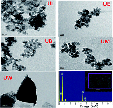 |
| | Fig. 1 TEM images of ZnO nanostructures prepared by low frequency ultrasound using various organic solvents (a–f). EDS spectrum of UW sample (g). | |
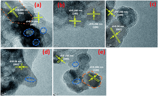 |
| | Fig. 2 HRTEM images of prepared ZnO nanostructures (a) UI, (b) UE, (c) UB, (d) UM and (e) UW. | |
Based on the experimental results, the various stages involved in the formation of ZnO nanostructures under precipitation conditions are outlined below:36
In the presence of an aqueous medium (organic solvents and water)
The addition of NaOH solution into the zinc acetate solutions causes the reactions
| Zn(OH)42− ↔ ZnO + H2O + 2OH− |
The organic solvents play an important role in the formation of ZnO nanostructures. Spherical particles were obtained when the organic solvents were used to prepare ZnO, and triangular structures were obtained when water was used as a solvent. This is due to the difference in the polarity of the solvents. The water has a stronger polarity than any of the organic solvents; the relatively weak polarity of the organic solvents may limit ZnO growth along the c-axis and favour isotropic growth. Similar kinds of results have been reported by Yan et al.37 in which ethanol–water mixtures have been used to control the morphologies of ZnO nanostructures. The schematic representation of the growth mechanism is shown in Fig. 3.
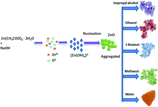 |
| | Fig. 3 Schematic illustration of the possible formation process for the ZnO nanostructures. | |
Specific surface area (SSA) is one of the important microstructural parameters of materials in determining the nature of porosity, and it is of considerable interest in the fields of catalysis, sensors, filters and pharmaceuticals.38 Fig. 4 represents the nitrogen adsorption desorption isotherms of the prepared ZnO nanostructures. The obtained values for BET surface areas are 29, 40, 49, 62, 65 m2 g−1 corresponding to UW, UI, UB, UM, and UE, respectively; considerable changes have been observed by changing reaction medium.
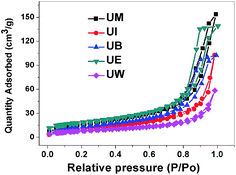 |
| | Fig. 4 Nitrogen adsorption desorption isotherms for the ZnO nanostructures. | |
XRD patterns of the prepared ZnO nanostructures are shown in Fig. 5. All the XRD patterns of ZnO nanostructures show strong and broad peaks which confirm the wurtzite structure of ZnO at the nanoscale. The peaks are located at the angles (2θ) of 31.79, 34.45 and 36.30° which correspond to the (100), (002) and (101) planes, respectively, of ZnO (JCPDS no: 01-089-1397). The other peaks are found at 2θ angles of 47.57, 56.63, 62.91, 66.39, 68.01 69.14, 72.51 and 76.86° corresponding to the (102), (110), (103), (200), (112), (201), (004) and (202) planes of the wurtzite structure, respectively. The UI and UW samples show a peak located at 33.1° which corresponds to the zinc hydroxide phase. The broadening of the FWHM was dependent on the size and shape of the nanostructures, and the crystallite size was estimated using the Debye–Scherrer formula.39 The obtained values were found to be ∼13, 15, 17, 21, and 38 nm corresponding to UE, UI, UB, UM and UW samples, respectively.
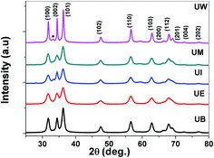 |
| | Fig. 5 XRD patterns of the ZnO nanostructures prepared using different solvents. * indicates the zinc hydroxide phase. | |
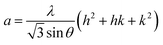
In general, the lattice parameters of semiconductor nanostructures depend on the concentration of dopant ion, structural defects, external strain and the difference of dopant ionic radius with respect to the host matrix ion.3 The lattice parameters, ‘a’ axis, ‘c’ axis and unit cell volume ‘v’, were calculated through the following relations:39
| |
 | (1) |
| |
 | (2) |
and
| |
 | (3) |
The calculated lattice parameters ‘a’, ‘c’ and ‘v’ are shown in Fig. 6(a–c). In the present study, the differences in defects and microstrain in the samples cause a variation in the lattice constants.
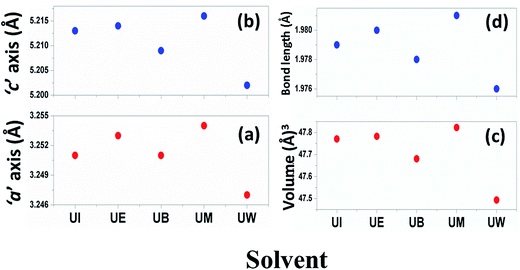 |
| | Fig. 6 Variations of lattice parameters with the different solvents: (a) ‘a’ axis; (b) ‘c’ axis; (c) unit cell volume; and (d) bond length. | |
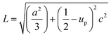
The solvent effect on the ZnO bond length was analysed and is shown in Fig. 6(d). The bond length was calculated by using the relation:40
| |
 | (4) |
where, ‘
a’, and ‘
c’ are lattice parameters and ‘
up’ is the positional parameter which is a measure of the amount by which each atom is displaced with respect to the next, along the ‘
c’ axis. ‘
up’ can be calculated by the formula:
3| |
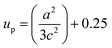 | (5) |
The variation of Zn–O bond length in the different solvents is shown in Fig. 6(d).
Microstructural calculations
X-ray profile analysis is a simple and powerful technique to quantify the crystallite size and lattice strain. Williamson–Hall proposed that the broadening of a diffraction line is due to the combination of the crystallite size and strain as a function of the diffraction angle and can be written in the form of a mathematical expression:41where, βt is due to the crystallite size contribution, βε is due to strain induced broadening and βhkl is the width of the half maximum intensity of the individual diffracted peak. The width of each diffraction line is a combined effect of both instrumental and sample contributions. In order to decompose line broadening effects from the instrumental contribution, a standard silicon (Si) sample was used. The instrumental corrected line broadening of each diffraction peak was calculated through the relation:42| | |
βhkl = [(βhkl)measured2 − βinstrumental]0.5
| (7) |
where, βinstrumental is the broadening due to the instrumental contribution. The diffraction peaks were fitted using the Pearson VII function to calculate the FWHM. The crystallite size (t) contribution can be calculated by using the Scherrer formula:41| |
 | (8) |
where, k is the shape factor, λ is the wavelength of the X-ray used (0.154056 nm) and βt is the FWHM of the diffracted peak. Similarly, the strain contribution can be evaluated by the relation:41| |
βε = 4ε![[thin space (1/6-em)]](https://www.rsc.org/images/entities/char_2009.gif) tanθ tanθ
| (9) |
where, ‘ε’ is the microstrain. It is clear that the line broadening is a combination of the crystallite size and strain contribution, and it is represented by the mathematical formula:41| |
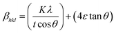 | (10) |
This can be further simplified as follows:
| |
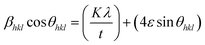 | (11) |
The calculated value of βhklcosθhkl as a function of 4sinθhkl is plotted and is shown in ESI Fig. 3.† This model is known as the uniform deformation model (UDM).
In UDM, microstrain (ε) is assumed to be isotropic (uniform in all the crystallographic directions), but this assumption is no longer valid since the microstructural properties vary with the crystallographic directions. Microstrain can be correlated with stress, which is directionally dependent. In the uniform deformation stress model (UDSM), the uniform deformation stress (σ) is expressed as:
where,
Ehkl is the Young's modulus in the direction perpendicular to the (
hkl) plane and
εhkl is the anisotropic microstrain, dependent on the crystallographic directions. For the hexagonal crystals, the Young's modulus could be obtained through the following relation:
43| |
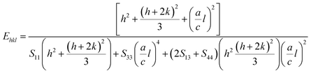 | (13) |
where, ‘
a’ and ‘
c’ are lattice parameters and
S11,
S33,
S13 and
S44 are the elastic compliances of ZnO. The values of the elastic compliances are 7.858 × 10
−12, −2.206 × 10
−12, 6.940 × 10
−12 and 23.57 × 10
−12 respectively.
44 In the UDSM model, the W–H equation becomes:
| |
 | (14) |
σ can be obtained estimated from the slope of the linear fit of the graph which is plotted between βhklcosθhkl and 4sinθ/Ehkl, and is shown in ESI Fig. 4.† Fig. 7 depicts the variation of microstrain and stress with the solvents. Similarly, the Young's modulus and εhkl are connected to the density of deformation energy ‘u’ through the relation:42
| |
 | (15) |
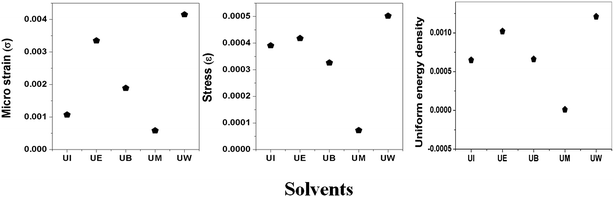 |
| | Fig. 7 Variation of microstrain, stress, and uniform energy density with the different solvents. | |
Substituting eqn (15) into eqn (11), the W–H relation becomes:
| | |
βhklcosθhkl = (25/2sinθhklE−1/2hkl)u1/2
| (16) |
The value ‘u’ can be obtained from the plot between 25/2sinθhklE−1/2hkl vs. βhklcosθhkl which is shown in ESI Fig. 5,† and the value of uniform energy density is shown in Fig. 7. This model is known as the uniform deformation energy density model (UDEDM).
Vibrational properties
Raman spectra. Raman spectroscopy is a non-destructive testing tool used to study the vibrational properties of bulk/nanostructured materials, and specifically to identify dopant ions in the lattice plane, secondary phase formation, and structural disorder properties of nanostructures.45 Wurtzite type ZnO is a II–VI wide band gap semiconductor belonging to the space group C6v4, with two formula units in the primitive cell.32 According to group theory analysis, the zone centre optical phonons can be classified to the following irreducible representation: Γopt = A1 + E1 + 2E2 + 2B1, where A1 and E1 modes are polar modes and both Raman and infrared active, and they can split into transverse optical (TO) and longitudinal optical (LO) phonons. The Raman active phonon of the A1 branch is polarized in the z-direction, whereas the E1 branch is polarized in the xy plane.33 E2 modes are only Raman active, non-polar modes and they have two wavenumbers, one with low frequency (Elow2) associated with the vibrations of the Zn sub-lattice and one with high frequency (Ehigh2) associated with the motion of oxygen atoms only. The B1 modes are both Raman and infrared inactive and are known to be silent modes.In order to investigate the influence of size and shape on the Raman scattering of ZnO nanostructures, the room temperature non-resonant Raman scattering of all samples was measured in the range 50 to 2000 cm−1 and the spectra are shown in Fig. 8(a–e). According to DFT calculations, the second order phonon modes are divided into three regions: (i) the frequency range between 160 and 540 cm−1 is associated with acoustic overtones, (ii) the frequency range between 540 and 820 cm−1 is attributed to the combinations of optical and acoustic phonon modes, and (iii) the high frequency region between 820 and 1120 cm−1 is formed by optical overtones and combinations.32 To identify the individual phonon modes, each Raman spectrum was fitted using the Lorentzian function and the decomposed spectrum of the UB sample is shown in Fig. 7(f). The characteristic Raman bands of the wurtzite ZnO lattice, located at 98 and 437 cm−1, are assigned to Elow2 and Ehigh2 respectively. The band appearing at ∼330 cm−1 is ascribed to the difference Ehigh2 − Elow2 which is known to be due to multiphonon scattering. The peaks at 532, 547, and 551 cm−1 are clearly of A1 symmetry and can be attributed to the 2Blow1 and LA overtones. The reason for the observation of B1 silent modes and second order phonon modes are due to the breakdown of the translational symmetry of the lattice caused by defects or impurities which arise because of either the dopant nature or the growth conditions.30 The phonon modes located at 699, 732, and 755 cm−1 can be ascribed to the combinations of acoustic and optical phonons of A1 symmetry. Similarly, a three phonon combination mode, appearing in the higher frequency region at ∼1431 cm−1, is ascribed to the A1 (long) + E1 (transv) + E2 process.35 Two phonon combinations modes, located at 679 and ∼835 cm−1, could be assigned to the vibrations of A1 (long) + E2 and E1 (transv) + E2 respectively. The second order multiphonon scattering mode, appearing at ∼935 cm−1, could be assigned to the vibrations from 2E2H + E2L. The phonon frequency observed at higher wavenumber is known to be from a second order Raman process; in the present case, the peak observed at ∼1140 cm−1 is assigned to the 2LO vibrations. Fig. 9 represents the variations of microstrain and the Ehigh2 mode in the different samples. In general, the Ehigh2 mode is highly sensitive to the lattice strain. The increase of the lattice parameter c leads to tensile strain along the c-axis which causes a blue shift, and similarly a decrease of the lattice parameter c causes a compressive strain along the c-axis which results in a red shift of the Ehigh2 phonon mode (Table 1).31
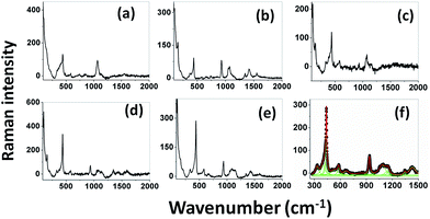 |
| | Fig. 8 Room temperature non resonant Raman spectra of UE (a), UI (b), UW (c), UM (d), and UB (e) ZnO nanostructures. Lorentzian decomposed Raman spectrum of UB sample (f). | |
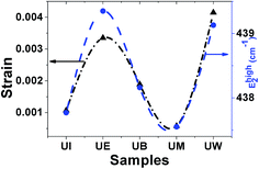 |
| | Fig. 9 Variation of microstrain vs. the EHigh2 mode. | |
Table 1 Phonon vibrational bands, assignments and symmetries of the first order, second order and multiphonon Raman scattering of the ZnO nanostructuresa
| UE, cm−1 |
UI, cm−1 |
UM, cm−1 |
UB, cm−1 |
UW, cm−1 |
Ref. |
Symmetry |
Process |
| Our results are compared to the Raman wavenumbers taken from Cusco et al.,32 and Kunert et al.35 |
| 99 |
98 |
98 |
99 |
98 |
99 |
E2 |
Elow2 |
| 339 |
333 |
330 |
330 |
334 |
333 |
A1, (E2, E1) |
Ehigh2 − Elow2 |
| 376 |
375 |
386 |
399 |
396 |
378 |
A1 |
A1 (TO) |
| 413 |
420 |
421 |
423 |
423 |
410 |
E1 |
E1 (TO) |
| 439 |
437 |
437 |
438 |
439 |
438 |
E2 |
Ehigh2 |
| 483 |
— |
483 |
— |
484 |
483 |
A1 |
2LA |
| 551 |
— |
— |
532 |
547 |
541 |
A1 |
2Blow1; 2LA |
| — |
576 |
574 |
579 |
— |
574 |
A1 |
A1 (LO) |
| 582 |
— |
— |
— |
581 |
584 |
E1 |
E1 (LO) |
| — |
— |
— |
669 |
— |
666 |
A1 |
TA + LO |
| — |
— |
— |
— |
679 |
679 |
Two phonon combinations |
A1 (long) + E2 |
| — |
— |
699 |
— |
— |
700 |
A1 |
LA + TO |
| 732 |
755 |
— |
— |
— |
745 |
A1 |
LA + TO |
| 847 |
— |
— |
835 |
859 |
845 |
Two phonon combinations |
E1 (transv) + E2 |
| — |
930 |
934 |
935 |
932 |
950 |
Second order multiphonon scattering |
2E2H + E2L |
| — |
1050 |
— |
— |
— |
1044 |
A1 |
TO + LO |
| 1067 |
1073 |
1074 |
1080 |
1068 |
1072 |
A1 |
TO + LO |
| 1139 |
1122 |
1140 |
1154 |
1144 |
1158 |
A1 |
2A1 (LO); 2E1 (LO); 2LO |
| |
1421 |
1444 |
1431 |
1432 |
1425 |
Three phonon combinations |
A1 (long) + E1 (transv) + E2 |
Phonon life time. The phonon life time (τ) can be deduced from the Raman scattering by using the energy–time uncertainty relation 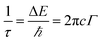 where, ΔE is the uncertainty in the energy of the phonon mode, ℏ is the Planck constant, and Γ is the FWHM of the Raman modes in cm−1.32 The phonon life time is a combination of two characteristic decay times such as the anharmonic decay of the phonon into two or more phonons so that energy and momentum are conserved (τA) and the perturbation of the translational symmetry of the crystals due to the presence of impurities, defects and isotopic fluctuations (τl). Thus the calculated phonon life time is an addition of these two characteristics decay times
 . The calculated phonon life time values are listed in Table 2.
Table 2 Phonon life time measurements for ZnO nanostructures
| Phonon mode |
UE |
UI |
UM |
UB |
UW |
| Γ (cm−1) |
τ (ps) |
Γ (cm−1) |
τ (ps) |
Γ (cm−1) |
τ (ps) |
Γ (cm−1) |
τ (ps) |
Γ (cm−1) |
τ (ps) |
| Elow2 |
7.92 |
0.67 |
7.37 |
0.719 |
7.83 |
0.677 |
7.81 |
0.679 |
6.667 |
0.795 |
| Ehigh2 − Elow2 |
19.56 |
0.271 |
9.11 |
0.582 |
28.84 |
0.1839 |
45.94 |
0.1154 |
24.87 |
0.213 |
| A1 (TO) |
43.61 |
0.121 |
58.12 |
0.091 |
73.94 |
0.071 |
52.75 |
0.1005 |
102.565 |
0.052 |
| E1 (TO) |
42.62 |
0.124 |
27.68 |
0.192 |
27.78 |
0.191 |
25.57 |
0.207 |
34.69 |
0.1528 |
| Ehigh2 |
16.08 |
0.329 |
11.6 |
0.457 |
11.45 |
0.463 |
11.85 |
0.447 |
12.09 |
0.438 |
| 2LA |
4.08 |
1.301 |
— |
— |
4.39 |
1.208 |
— |
— |
7.939 |
0.668 |
| 2Blow1; 2LA |
35.6 |
0.148 |
— |
— |
— |
— |
93.45 |
0.056 |
92.74 |
0.057 |
| A1 (LO) |
— |
— |
16.588 |
0.319 |
28.91 |
0.183 |
27.07 |
0.196 |
— |
— |
| E1 (LO) |
12.57 |
0.422 |
— |
— |
— |
— |
— |
— |
22.41 |
0.237 |
| 2E2H + E2L |
— |
— |
17.81 |
0.297 |
21.38 |
0.248 |
21.76 |
0.244 |
13.33 |
0.398 |
| TO + LO |
37.37 |
0.142 |
29.01 |
0.183 |
71.95 |
0.073 |
90.81 |
0.058 |
46.46 |
0.114 |
| 2A1 (LO); 2E1 (LO); 2LO |
21.15 |
0.25 |
66.89 |
0.079 |
51.36 |
0.103 |
41.4 |
0.128 |
60.89 |
0.087 |
| A1 (long) + E1 (transv) + E2 |
— |
— |
63.06 |
0.084 |
180.19 |
0.029 |
65.27 |
0.055 |
378.8 |
0.014 |
FTIR spectra. The recorded FTIR spectra of the prepared ZnO nanostructures are displayed in Fig. 10. Usually in inorganic species, the vibrational motions lie in the wavenumber range <600 cm−1, and vibrational motion at higher wavenumbers can be assigned to organic species. All the spectra show an absorbance band at ∼460 cm−1 which is assigned to the E1 (TO) mode vibrations of ZnO.39 The broad bands at around ∼3400 and ∼1620 cm−1 could be assigned to the stretching and bending vibrations of H–O–H bonds, respectively.46 The bands observed at ∼1350–1450 and ∼1550 cm−1 are assigned to the symmetric and asymmetric stretching vibrations of COO− modes from the carboxyl groups of the acetate in the metal precursors.
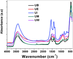 |
| | Fig. 10 FTIR spectra of the ZnO nanostructures prepared using different solvents. | |
Optical properties
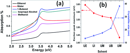
Absorption spectra. The optical absorption spectra of the samples prepared using various solvents are shown in Fig. 11(a). The peaks appearing at 3.422, 3.576, 3.58, 3.601 and 3.622 eV correspond to the samples UW, UM, UB, UE and UI respectively, and are due to the free excitonic absorption of the ZnO nanostructures. All the samples exhibit an excitonic peak shift as compared with the bulk ZnO absorption (3.37 eV) which is due to the quantum confinement effect. The ESI Fig. 5† clearly shows that there is band gap tuning due to the variation in the particle size. Previous reports have revealed that the band structure of the ZnO is size dependent and the particle size strongly influences the energetic position of the band edges.2 The band gap is inversely proportional to the size of the particles through the relation:2| |
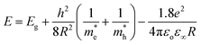 | (17) |
where, Eg is the bulk band gap, R is the particle size, m*e is the effective mass of the electron, m*h is the effective mass of the hole, ‘e’ is the charge of the electron and ‘ε∞’ is the high frequency dielectric constant. The correlation of the calculated band gap values versus particle size using eqn (17) is shown in ESI Fig. 4,† and this reveals the shifts in the band edges as a function of particle size. The variation of the excitonic peak maximum and crystallite size in the different solvents is shown in Fig. 11(b). This clearly shows that the band edge varies with respect to the particle size.
 |
| | Fig. 11 (a) Absorption spectra of the ZnO nanostructures prepared using different solvents. (b) Variation of the exciton peak maximum and crystallite size as a function of the solvent. | |
Photoluminescence spectra. In general, ZnO nanostructures have two emission bands, the relatively weak and narrow ultra violet (UV) emission band and the much stronger, broader emission band located at around 400–600 nm.47 Several works both theoretically and experimentally have reported the mechanism behind the origin of the broad visible emission from ZnO.48 The origin of the visible emission is due to the recombination of a photogenerated electron from a shallow level which is very close to the conduction band with the deep traps in the single ionized oxygen vacancy sites and/or the single negatively charged interstitial oxygen ions. This visible emission has a longer life time than the UV emission, in the order of microseconds .49 The UV emission band arises due to the radiative annihilation of excitons and the life time of this emission is very short, in the order of picoseconds. The PL spectra of ZnO nanostructures prepared using different solvents are shown in Fig. 12(a). The spectra show two emission bands, the first at around 385 nm, with low intensity, and the second centred at ∼530 nm with a broad band. These are assigned to the near band edge emission (NBE) and visible emission, respectively. The relative intensity of the visible to the UV emission (Ivis/IUV) strongly depends on the size of the particles, as shown in Fig. 12(b).
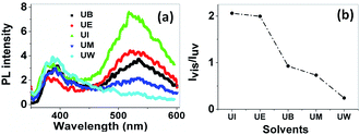 |
| | Fig. 12 (a) PL spectra of the prepared samples at an excitation wavelength of 330 nm. The band at 385 nm is from near band edge emission, and the broad band at 530 nm is due to deep level trap emission. (b) The relative intensity variation of visible to UV emission with respect to the solvents. | |
The variation of intensity ration of visible to UV emission is indicated in Fig. 12(b). It is clear that the ZnO nanoparticles prepared using isopropanol show a much higher intensity for the visible emission band than the exciton emission band. Interestingly, the visible emission band is gradually decreased for the samples prepared using ethanol, 1-butanol, and methanol and is completely absent for the UW samples. This phenomenon can be explained using size effects. The band appearing below the conduction band edge (2 eV) is assumed to be the recombination centre Vo+ for the visible emission. The recombination of a conduction band electron with a Vo++ centre can yield a photon with energy of 2 eV. The Vo++ centre can be created by the trapping of a hole in the Vo+ centre, and the probable hole trapping site is on the surface of the particles.50 When the particle possesses a large surface to volume ratio, efficient and fast trapping of photogenerated holes results at surface sites. The rate of the surface trapping process and defect concentration decreases as the particle size increases due to the decrease of surface to volume ratio.48 In the present case, the UI sample exhibits a high intensity visible emission band, this is gradually decreased for UE, UB and UM and is completely absent for UW samples. This is because of the reduction of possible trapping surface sites which results in the decrease of visible emission band intensity.
Conclusion
In summary, ZnO nanostructures were prepared by the low frequency (42 kHz) ultrasound route using various organic solvents as the reaction media. Lattice and microstructural parameters such as microstrain, stress, and energy density of the prepared ZnO nanostructures were extracted from X-ray diffraction (XRD) analysis. TEM images revealed morphological changes involving a spherical to triangular shaped structure, and the size of the nanoparticles was found to be dependent on the organic solvent used. Raman spectral measurements revealed that the changes in the phonon mode are due to the variation of microstrain and the presence of multiphonon scattering. The intensity of the visible emission band was found to vary with the particles' size and morphology. The strongest visible emission band corresponded to the smallest size with the largest surface/volume ratio. This could be attributed to the trapping of surface oxygen vacancies.
Acknowledgements
The authors gratefully acknowledge the FONDECYT-CONICYT (Projects No: 3140178 and No. 1130916) Government of Chile, Santiago, for financial assistance.
References
- C. F. Klingshirn, A. Waag, A. Hoffmann and J. Geurts, Zinc Oxide: From Fundamental Properties Towards Novel Applications, Springer, Heidelberg, Dordrecht, Lodon, New York, 2010, ISBN 978364210577–7 Search PubMed.
- A. van Dijken, E. A. Meulenkamp, D. Vanmaekelbergh and A. Meijerink, J. Phys. Chem. B, 2000, 104, 1715–1723 CrossRef CAS.
- Ü. Özgür, Y. I. Alivov, C. Liu, A. Teke, M. A. Reshchikov, S. Doan, V. Avrutin, S.-J. Cho and H. Morkoç, J. Appl. Phys., 2005, 98, 041301 CrossRef.
- D. Costenaro, F. Carniato, G. Gatti, L. Marchese and C. Bisio, New J. Chem., 2013, 37, 2103–2109 RSC.
- W. J. E. Beek, M. M. Wienk and R. A. J. Janssen, Adv. Mater., 2004, 16, 1009–1013 CrossRef CAS.
- M. Chen, L. Hu, J. Xu, M. Liao, L. Wu and X. Fang, Small, 2011, 7, 2449–2453 CAS.
- B. Zhao, F. Wang, H. Chen, Y. Wang, M. Jiang, X. Fang and D. Zhao, Nano Lett., 2015, 15, 3988–3993 CrossRef CAS PubMed.
- D. Jassby, J. F. Budarz and M. Wiesner, Environ. Sci. Technol., 2012, 46, 6934–6941 CrossRef CAS PubMed.
- V. Chivukula, D. Ciplys, M. Shur and P. Dutta, Appl. Phys. Lett., 2010, 96, 233512 CrossRef.
- K. R. Raghupathi, R. T. Koodali and A. C. Manna, Langmuir, 2011, 27, 4020–4028 CrossRef CAS PubMed.
- L. Xu, Y. L. Hu, S. Sithambaram, C. Pelligra, M. Aindow, C. H. Chen, R. Joesten, L. Jin, H. Huang and S. L. Suib, Chem. Mater., 2009, 21, 2875–2885 CrossRef CAS.
- B. Cheng and E. T. Samulski, Chem. Commun., 2004, 986, 986–987 RSC.
- X. Zhao and L. Qi, Nanotechnology, 2012, 23, 235604 CrossRef PubMed.
- R. Siddheswaran, R. V. Mangalaraja, Ricardo E. Avila, D. Manikandan, C. Esther Jeyanthi and S. Ananthakumar, Mater. Sci. Eng., A, 2012, 558, 456–461 CrossRef CAS.
- A. K. Zak, W. H. abd Majid, H. Z. Wang, R. Yousefi, A. M. Golsheikh and Z. F. Ren, Ultrason. Sonochem., 2013, 20, 395–400 CrossRef PubMed.
- S. Baruah and J. Dutta, J. Cryst. Growth, 2009, 311, 2549–2554 CrossRef CAS.
- H. Zhang, D. Yang, X. Ma, Y. Ji, J. Xu and D. Que, Nanotechnology, 2004, 15, 622–626 CrossRef CAS.
- A. C. Cakir and S. E. Ela, Adv. Powder Technol., 2012, 23, 655–660 CrossRef CAS.
- S. K. Na Ayudhya, P. Tonto, O. Mekasuwandumrong, V. Pavarajarn and P. Praserthdam, Cryst. Growth Des., 2006, 6, 2446–2450 Search PubMed.
- J. M. Patete, X. Peng, C. Koenigsmann, Y. Xu, B. Karn and S. S. Wong, Green Chem., 2011, 13, 482–519 RSC.
- M. Ghosh, D. Karmakar, S. Basu, S. N. Jha, D. Bhattacharyya and S. C. G. Gupta, J. Phys.
Chem. Solids, 2014, 75, 543–549 CrossRef CAS.
- C. R. Chandraiahgari, G. D. Bellis, P. Ballirano, S. K. Balijepalli, S. Kaciulis, L. Caneve, F. Sarto and M. S. Sarto, RSC Adv., 2015, 5, 49861–49870 RSC.
- G. Clavel, M. G. Willinger, D. Zitoun and N. Pinna, Adv. Funct. Mater., 2007, 17, 3159–3169 CrossRef CAS.
- Q. R. Hu, S. L. Wang, P. Jiang, H. Xu, Y. Zhang and W. H. Tang, J. Alloys Compd., 2010, 496, 494–499 CrossRef CAS.
- K. L. Foo, M. Kashif, U. Hashim and W. W. Liu, Ceram. Int., 2014, 40, 753–761 CrossRef CAS.
- X. Fang, L. Hu, C. Ye and L. Zhang, Pure Appl. Chem., 2010, 82, 2185–2198 CrossRef CAS.
- T. Andelman, G. Neumark, Y. Gong, M. Polking, S. O. Brien, M. Yin and I. Kuskovsky, J. Phys. Chem. B, 2005, 109, 14314–14318 CrossRef CAS PubMed.
- C. Ye, X. Fang, Y. Hao, X. Teng and L. Zhang, J. Phys. Chem. B, 2005, 109, 19758–19765 CrossRef CAS PubMed.
- A. Pimentel, J. Rodrigues, P. Duarte, D. Nunes, F. M. Costa, T. Monteiro, R. Martins and E. Fortunato, J. Mater. Sci., 2015, 50, 5777–5787 CrossRef CAS.
- F. J. Manjon, B. Mari, J. Serrano and A. H. Romero, J. Appl. Phys., 2005, 97, 53516 CrossRef.
- M. Scepanovic, M. G. Brojcin, K. Vojisavljevic, S. Bernik and T. Sreckovic, J. Raman Spectrosc., 2010, 41, 914–921 CrossRef CAS.
- R. Cuscó, E. Alarcón-Lladó, J. Ibáñez and L. Artús, Phys. Rev. B: Condens. Matter Mater. Phys., 2007, 75, 165202 CrossRef.
- H. K. Yadav, K. Sreenivas, R. S. Katiyar and V. Gupta, J. Phys. D: Appl. Phys., 2007, 40, 6005–6009 CrossRef CAS.
- R. S. Zeferino, M. B. Flores and U. Pal, J. Appl. Phys., 2011, 109, 014308 CrossRef (1–6).
- H. W. Kunert, D. J. Brink, F. D. Auret, J. Malherbe, J. Barnas and V. Kononenko, Phys. Status Solidi C, 2005, 2, 1131–1136 CrossRef CAS.
- Y. F. Zhu, G. H. Zhou, H. Y. Ding, A. H. Liu, Y. B. Lin and N. L. Li, Phys. E, 2010, 42, 2460–2465 CrossRef CAS.
- Z. Yan, Y. Ma, D. Wang, J. Wang, Z. Gao and T. Song, J. Phys. Chem. C, 2008, 112, 9219–9222 CAS.
- J. Becker, K. R. Raghupathi, J. S. Pierre, D. Zhao and R. T. Koodali, J. Phys. Chem. C, 2011, 115, 13844–13850 CAS.
- C. Suryanarayana and M. Grant Norton, X-ray diffraction: a practical approach, Plenum Press, New York, 1998, p. 213 Search PubMed.
- X. S. Wang, Z. C. Wu, J. F. Webb and Z. G. Liu, Appl. Phys. A, 2003, 77, 561–565 CrossRef CAS.
- V. Biju, N. Sugathan, V. Vrinda and S. L. Salini, J. Mater. Sci., 2008, 43, 1175–1179 CrossRef CAS.
- Y. Rosenberg, V. S. Machavariani, V. Voronel, S. Garber, A. Rubshtein, A. I. Frenkel and E. A. Stern, J. Phys.: Condens. Matter, 2000, 12, 8081–8088 CrossRef CAS.
- J. M. Zhang, V. Zhanga, K. W. Xub and V. Jic, Solid State Commun., 2006, 139, 87–91 CrossRef CAS.
- J. F. Nye, Physical properties of crystals: their representation by tensors and matrices, New York, Oxford, 1985 Search PubMed.
- T. Pandiyarajan and B. Karthikeyan, J. Raman Spectrosc., 2013, 44, 1534–1539 CrossRef CAS.
- T. Gruber, G. M. Prinz, C. Kirchner, R. Kling, F. Reuss, W. Limmer and A. Waag, J. Appl. Phys., 2004, 96, 289–293 CrossRef CAS.
- A. Sahai and N. Goswami, Phys. E, 2014, 58, 130–137 CrossRef CAS.
- A. B. Djurisic and Y. H. Leung, Small, 2006, 2, 944–961 CrossRef CAS PubMed.
- A. van Dijken, E. A. Meulenkamp, D. Vanmaekelbergh and A. Meijerink, J. Phys. Chem. B, 2000, 104, 1715–1723 CrossRef CAS.
- A. van Dijken, E. A. Meulenkamp, D. Vanmaekelbergh and A. Meijerink, J. Lumin., 2000, 90, 123–128 CrossRef CAS.
Footnote |
| † Electronic supplementary information (ESI) available. See DOI: 10.1039/c5ra27147a |
|
| This journal is © The Royal Society of Chemistry 2016 |
Click here to see how this site uses Cookies. View our privacy policy here. 


 where, ΔE is the uncertainty in the energy of the phonon mode, ℏ is the Planck constant, and Γ is the FWHM of the Raman modes in cm−1.32 The phonon life time is a combination of two characteristic decay times such as the anharmonic decay of the phonon into two or more phonons so that energy and momentum are conserved (τA) and the perturbation of the translational symmetry of the crystals due to the presence of impurities, defects and isotopic fluctuations (τl). Thus the calculated phonon life time is an addition of these two characteristics decay times
 . The calculated phonon life time values are listed in Table 2.


