
Synthesis of β-SiC nanowires via a facile CVD method and their photoluminescence properties†
Silin Liua,
Haitao Liua,
Zhaohui Huang*a,
Minghao Fanga,
Yan-gai Liua and
Xiaowen Wuab
aSchool of Materials Science and Technology, Beijing Key Laboratory of Materials Utilization of Nonmetallic Minerals and Solid Wastes, National Laboratory of Mineral Materials, China University of Geosciences, Beijing, 100083, P. R. China. E-mail: silinliu0602@163.com
bDepartment of Mechanical Engineering, University College London, Torrington Place, London WC1E 7JE, UK
First published on 26th February 2016
Abstract
β-SiC nanowires with large scale have been synthesized successfully via a chemical vapour deposition (CVD) method at 1300 °C without using catalysts, templates or extra gases. X-ray diffraction (XRD), field emission scanning electron microscopy (FESEM), Fourier transform infrared spectroscopy (FT-IR) and energy-dispersive X-ray spectroscopy (EDS) were used to characterize the phase and the morphology of the as-prepared products. Characterization of the as-synthesized nanowires indicated that they were made up of a crystalline SiC core coated with an amorphous SiO2 shell. A vapor–solid (VS) growth mechanism was proposed for the growth mode of the as-grown SiC/SiO2 nanowires. The photoluminescence (PL) spectrum of as-obtained nanowires exhibited a significant blue shift compared with the bulk SiC. When the reaction temperature was changed (1200 °C, 1400 °C, 1500 °C), low production or irregular morphology of the nanowires was obtained. The diameter of nanowires synthesized with catalyst was narrower between 20–40 nm while that without catalyst was about 50 nm. The as-synthesized products have potential in future blue-green emitting device applications. This research will also be helpful in simplifying the synthesis of SiC-related nanostructures.
Introduction
One-dimensional (1D) nanostructured materials, such as nanowires, nanotubes, nanobelts, nanochains and nanocables, have attracted lots of attention for their excellent properties.1–5 Among these nanostructures, nanowires have become the main research objects due to their potential applications in electronic, optical and optoelectronic devices.6–8 The past decades have witnessed many efforts devoted to the growth of nanowires, for example, Ag nanowires,9 Ge nanowires,10 silicon carbide (SiC) nanowires,11 Si nanowiers12 and so on.SiC is a significant wide band gap (2.4 eV at room temperature) semiconductor.13 Two hundred crystalline forms have been found of SiC. Only one type of the forms belongs to cubic system, named 3C-SiC or β-SiC. The others are all hexagon, named α-SiC. β-SiC nanowires show imaging electronic, physical, and chemical properties causing them suitable for high temperature, high power, high frequency and high thermal conductivity environments.14–18 So far, lots of methods have been used to synthesize β-SiC nanowires. Fu et al.19 synthesized β-SiC nanowires using CH3SiCl3 as raw materials, H2 and Ar gases as protective gas and via a chemical vapour deposition (CVD) method at 1050–1150 °C without using metallic catalyst. Liang et al.20 prepared mesoporous silica containing Fe nanoparticles by the sol–gel process previously and heated the sol–gel solution at 1400 °C to get the β-SiC nanowires. Dai et al.21 synthesized β-SiC nanowires using Si–SiO2 powders as raw materials via a simple CVD method, and during the experiment, Ar gas was used to remove residual oxygen and the reaction temperature was 1460 °C. Nevertheless, most of these methods involve complicated equipment and processes with high temperature and spend more in raw materials or removing the metal catalyst when put the nanowires in application.
In this paper, large scale β-SiC nanowires are synthesized using Si–SiO2 powders as raw materials through a relatively facile CVD method at 1300 °C without using any gases (Ar, N2, CH4, etc.) or metallic catalysts. It may reduce costs in experiment or application.
Experiment
In our previous researches, a simplified CVD method was reported to synthesize β-SiC nanostructure.22,23 However, the output of the as-grown nanowires was little and the reaction temperature was high (1500 °C). In order to synthesize a large scale of β-SiC nanowires at lower cost, the reaction temperature was changed at 1300 °C. At the same time, the influence of temperature and catalyst to the products was also investigated. In this research, Si (200 mesh, Sinopharm Chemical Reagent Co., Ltd.) and SiO2 (200 mesh, Sinopharm Chemical Reagent Co., Ltd.) powders were used as raw materials. According to the chemical reaction equation (Si(s) + SiO2(s) → 2SiO(g)), 7 g Si and 15 g SiO2 powders were put into nylon ball milling tank with corundum ball (material![[thin space (1/6-em)]](https://www.rsc.org/images/entities/char_2009.gif) :corundum ball milling = 1:2). The Si–SiO2 mixture powders were gotten after 2 hours milling. 500 mg such mixture powders were put into a small cleaned graphite crucible and covered with the cleaned graphite felt (the surface of the graphite felt was ultrasonically cleaned with ethanol for 10 min and then dried in air.). Afterwards, the cleaned system was embedded in a larger enclosed corundum crucible filling with graphite powders as shown in Scheme 1. At the same time, a bit of holes were made by a needle in the clean graphite felt to keep the atmospheric pressure balance between the big enclosed corundum and the small graphite crucibles. After that, the above-mentioned big enclosed corundum crucible was heated in air atmosphere in a resistance furnace. The furnace temperature was initially raised to 1000 °C with a rate of 10 °C min−1, and then raising the temperature to 1300 °C at a heating rate of 3 °C min−1 and holding for 3 hours. When the temperature was naturally cooled down to the room temperature, a blue colored layer was gotten on the surface of the graphite felt.
:corundum ball milling = 1:2). The Si–SiO2 mixture powders were gotten after 2 hours milling. 500 mg such mixture powders were put into a small cleaned graphite crucible and covered with the cleaned graphite felt (the surface of the graphite felt was ultrasonically cleaned with ethanol for 10 min and then dried in air.). Afterwards, the cleaned system was embedded in a larger enclosed corundum crucible filling with graphite powders as shown in Scheme 1. At the same time, a bit of holes were made by a needle in the clean graphite felt to keep the atmospheric pressure balance between the big enclosed corundum and the small graphite crucibles. After that, the above-mentioned big enclosed corundum crucible was heated in air atmosphere in a resistance furnace. The furnace temperature was initially raised to 1000 °C with a rate of 10 °C min−1, and then raising the temperature to 1300 °C at a heating rate of 3 °C min−1 and holding for 3 hours. When the temperature was naturally cooled down to the room temperature, a blue colored layer was gotten on the surface of the graphite felt.
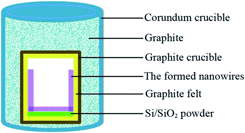 | ||
| Scheme 1 Schematic experimental setup for β-SiC nanowires synthesis. | ||
X-ray diffraction (XRD) with Cu Kα1 radiation (λ = 1.5406 Å) was conducted to identify the phase composition of the as-prepared products. Field emission scanning electron microscope (FESEM, LEO-1530, Germany) equipped with energy-dispersive X-ray spectroscopy (EDS) and transmission electron microscope (TEM/HRTEM, FEI-TECNAI G2, America) were used to characterize their morphology, chemical composition and microstructure. Fourier transform infrared (FT-IR) data was gained with a Nicolet IR100/200 spectrophotometer over the wavelength between 400 and 1300 cm−1. The photoluminescence (PL) property was performed at room temperature by using a fluorescence spectrophotometer (Hitachi F-4600, Japan) with Xe lamp excitation.
Results and discussion
Fig. 1a shows the digital camera picture of the as-prepared products. As shown in Fig. 1a, a light-blue layer of products is clearly seen on the graphite felt. The as-grown products show a large scale compared with previous experimental results.24,25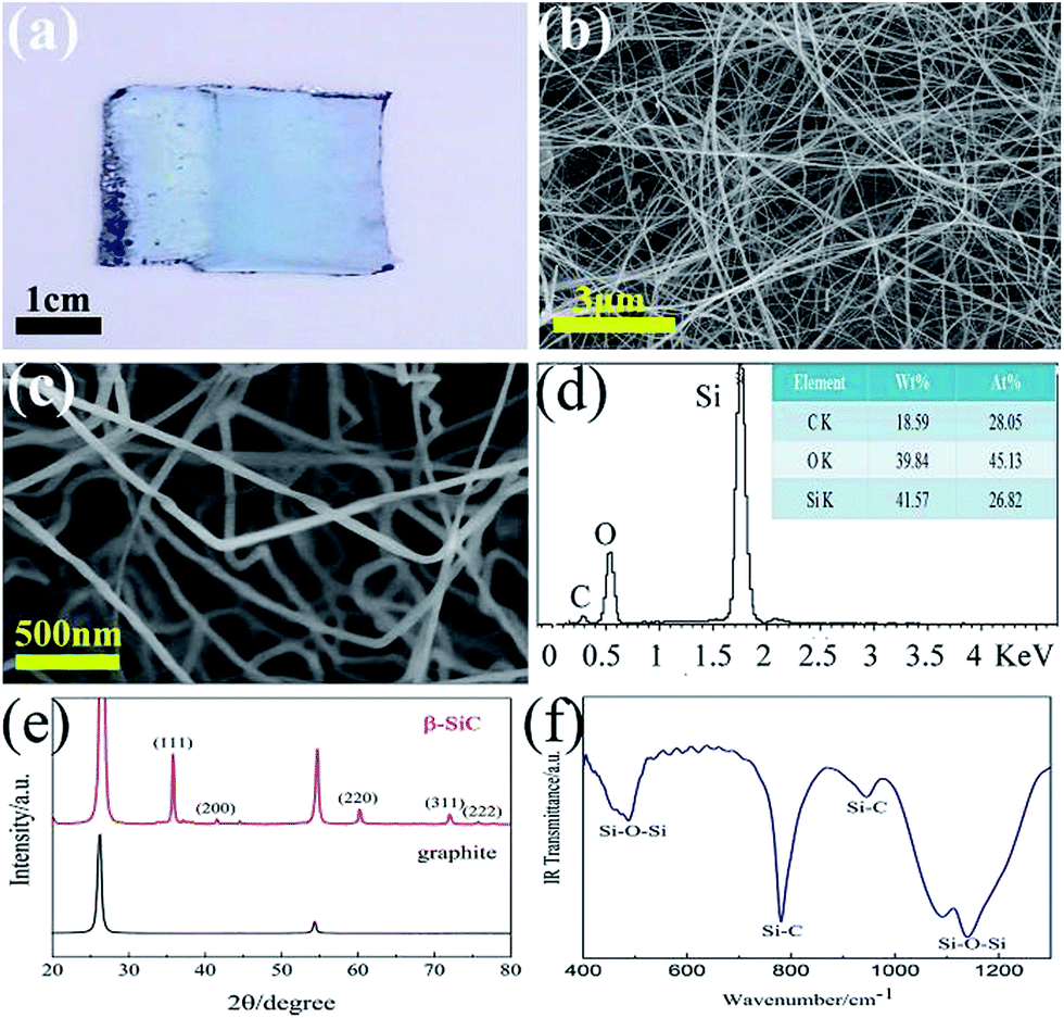 | ||
| Fig. 1 (a) Digital camera picture of blue wool-like products grown on the surface of graphite felt, (b) low magnification and (c) high magnification FESEM images of the as-grown product, (d) EDS pattern of the nanowires, (e) XRD pattern of as-synthesized products, (f) FT-IR absorption spectrum of as-synthesized products. | ||
Fig. 1b and c show the FESEM images of as-grown products. It can clearly be seen, the products are shown as one dimensional nanowire, which have long straight length (from twenty to hundreds of micrometres) and narrow diameter about 50 nm. The nanowires are irregular in direction, showing highly curved and good flexibility. Furthermore, as shown in Fig. 1c, the high magnification FESEM image illustrates these nanowires with high aspect ratio have a smooth surface. As can be observed, no metallic droplets are found at the top of the as-grown nanowires. Fig. 1d shows the EDS spectrum of the as-grown nanowires. The EDS analysis reveals that the nanowires are composed of Si, C and O. The atomic percentages of Si, C and O are about 26.82%, 28.05% and 45.13%.
XRD pattern, as shown in Fig. 1e, identifies the products are β-SiC compared with the JCPDS card no. 29-1129. In addition, the strong diffraction peaks at 26.6° and 54.79° are due to the graphite felt substrate.
At the same time, FT-IR is also used to identify the phase composition of the products. Fig. 1f shows the FT-IR absorption spectrum of as-synthesized products. The absorption peak at 780 cm−1 is related to the transversal optic (TO) Si–C stretching vibration and the peak at 946 cm−1 corresponds to the longitudinal optic (LO) vibration mode.1,23
In addition, the three absorption peaks arrange at around 450–500 cm−1 and 1000–1200 cm−1 correspond to Si–O–Si stretching vibration of amorphous SiO2.23,26,27
The detailed microstructure of the as-obtained nanowires is characterized by TEM/HRTEM. Fig. 2a and b and S1† show the typical TEM images of the nanowires. It is clearly seen the nanowires are consist of a crystal-core which the diameter of 20 nm and an amorphous-sheath with there exists stacking faults in the core. Combining with the data of XRD and SEM, it can be inferred that the core of the nanowires is crystalline SiC and the sheath is an amorphous SiO2 layer. Fig. 2c and d show the HRTEM images of the as-obtained nanowires at different magnification. The lattice fringes shown in Fig. 2d is 0.25 nm corresponded to the (111) plane spacing of β-SiC. The axis of the (111) crystal plane is consistent with the longitudinal direction of SiC nanowires, implying that the nanowires grow along the [111] direction. Combining with the XRD, FT-IR, TEM and EDS analyses, we roughly consider the nanostructure as-prepared is SiC nanowires coating with amorphous SiO2.
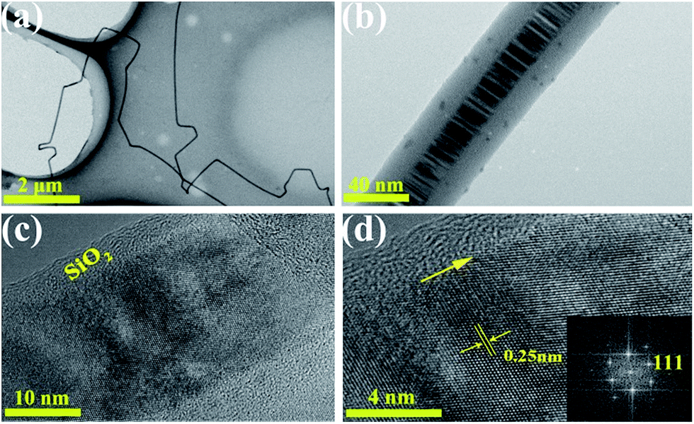 | ||
| Fig. 2 (a) and (b) Typical low and high magnification TEM images of as-grown SiC nanowires, (c) and (d) HRTEM images of the nanowires, the inset in (d) is the corresponding electron diffraction pattern of the SiC core. | ||
Furthermore, in order to characterize the influence of temperature in the process of preparing SiC nanowires, the same reaction setup is also heated at 1200 °C, 1400 °C and 1500 °C, respectively.
The digital camera pictures of the as-synthesized nanowires are shown in Fig. S2a–c.† No product is appeared in the graphite felt when heating at 1200 °C (as shown in Fig. S2a†). As shown in Fig. S2b and c,† when heating at 1400 °C or 1500 °C, few scattered products can be observed. Fig. 3 display the FESEM images of the as-grown products at 1400 °C and 1500 °C. It can be observed that the morphology of the products prepared at 1400 °C and 1500 °C are not as uniform as the products synthesizing at 1300 °C. The nanowires collected at 1500 °C have a larger diameter and lower aspect ratio compared with the products synthesized at 1300 °C. Therefore, we roughly consider that 1300 °C is an appropriate temperature in preparing of SiC nanowires via this facile CVD method.
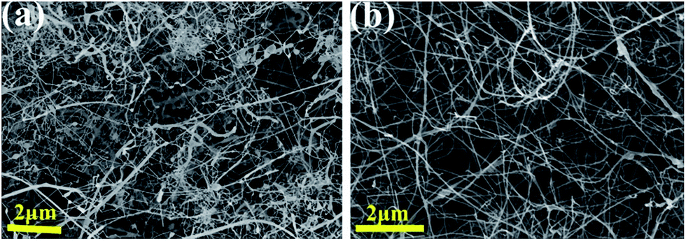 | ||
| Fig. 3 (a) Low magnification FESEM image of the nanowires synthesized at 1400 °C reaction temperature, and (b) at 1500 °C. | ||
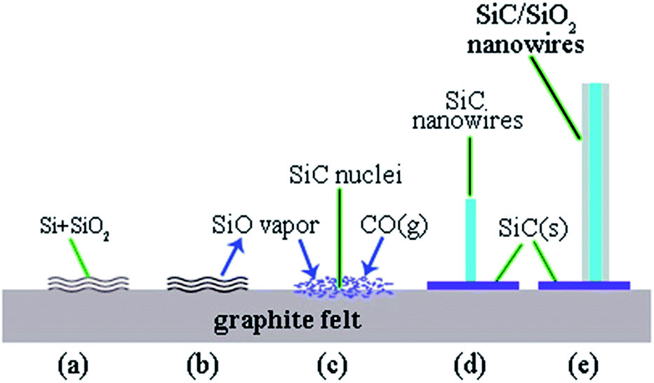
The traditional nanowires growth mechanism is vapor–liquid–solid (VLS) mechanism. In this mechanism, metallic catalyst will be used to assist the reaction. When the experiment finished, metallic catalyst droplets will be found in the top (VLS-tip growth mechanism) or base (VLS-base growth mechanism) of the nanowires. In our research, no metallic catalyst is introduced into the raw material. According to the TEM images, no catalyst droplet is found. At the same time, the existence of metal elements has not been found in the energy spectrum diagram. Thus completely rule out the possibility of VLS mechanism. In view of our experimental results, a vapour–solid (VS) growth mechanism (shown in Scheme 2) is inferred to explain the main growth mechanism for as-synthesized SiC/SiO2 nanowires.
 | ||
| Scheme 2 Schematic illustration of the possible growth mode for SiC/SiO2 nanowires. | ||
In our setup, graphite is used to supply carbon source and prevented the oxygen in the air from entering the corundum crucible, thus, forming an enclosed system. So, the source of the oxygen in this process is contributed to the SiO2 powders and O2 inside the furnace (detailed discussions). The O2 will react with the graphite powders to yield CO vapour straight by reaction (1).
| 2C(s) + O2(g) → 2CO(g) | (1) |
When the temperature rises gradually, SiO vapour is generated by the reaction of the SiO2 with Si powders according to the reaction (2).
| Si(s) + SiO2(s) → 2SiO(g) | (2) |
With the temperature increasing, the graphite powders are vaporized to C vapour.28 Then, according to the research of Chen et al.29 through the reaction (3) and (4), SiO also can be gotten.
| SiO2(s) + C(g) → SiO(g) + CO(g) | (3) |
| SiO2(s) + CO(g) → SiO(g) + CO2(g) | (4) |
Afterward, the SiO vapour obtained in the above-mentioned reactions further reacts with the graphite powders or CO vapour, according to the reaction (5) and (6) mentioned in.29
| SiO(g) + 2C(s) → SiC(s) + CO(g) | (5) |
| SiO(g) + 3CO(g) → SiC(s) + 2CO2(g) | (6) |
As interpreted in reaction (4) and (6), CO2 vapour can be generated in this enclosed system. The as-formed CO2 could re-react with the graphite powder or C vapour, and then re-generate CO gas. It can be inferred that the presence of CO2 is beneficial to the transfer of carbon source. According to the above reactions, SiC nuclei are obtained on the surface of the graphite substrate.
Fig. 4a shows a typical FESEM image, which displays the root of the nanowires (the place where the nuclei generated). Fig. 4b–d show the EDS spectra recorded at A, B and C marked in Fig. 4a, respectively. As shown in Fig. 4, the three locations all possess Si, C and O elements. Together with the above discussions, we believe that SiC nuclei are generated on the graphite, and then SiC nanowires are grown along [111] direction.
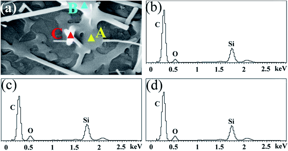 | ||
| Fig. 4 (a) High magnification FESEM image of the root of nanowires, (b), (c) and (d) EDS patterns of the root recorded from the marked areas A, B and C in (a) respectively. | ||
TEM observations indicated that the as-synthesized nanowires possess a SiC–SiO2 core–shell structure. On account of the higher melting point of SiC than that of SiO2,30–32 the solidification of the SiC core happens faster than that of the viscous SiO2 layer. Hence, the amorphous SiO2 layer will be formed and wraps the crystalline SiC nanowires during the cooling period. As previous reported,23 the generation of SiO2 according to the reaction (7) and (8).
| 2SiO(g) + C(g) → SiC(s) + SiO2(s) | (7) |
| 3SiO(g) + CO(g) → SiC(s) + 2SiO2(s) | (8) |
The PL spectrum (shown in Fig. 5) of as-obtained SiC/SiO2 nanowires is measured at room temperature under excitation at 254 nm from Xe source. The SiC/SiO2 nanowires show a broad emission peak in the blue region of the spectrum. Compared with the band gap of bulk β-SiC 2.4 eV (at room temperature),13 the emission peaks are apparently obvious blue-shifted in this research. Similar emission peak at about 416 nm was reported by Zhang et al.26 for the SiC/SiO2 nanowires, which may be attributed to the existence of oxygen defects in the amorphous layer, the special rough core–shell interface, and the morphology defects including stacking faults within the SiC nanostructures. SiC/SiO2 nanochain synthesized by Meng et al.17 showed a broad emission peak at 408 nm. They proposed that the wide PL peak may be owing to altering diameter of the nanostructures, stress at the SiC/SiO2 interface boundary, the size confinement effect and high density of defects including stacking faults within the SiC nanostructures. Therefore, it is presented that the blue-shift in our research might result from the stacking faults and the influence of the amorphous SiO2 layer.
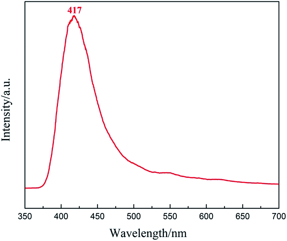 | ||
| Fig. 5 The room temperature PL spectrum of the as-obtained SiC/SiO2 nanowires. | ||
In previous studies, low melting point metals were often used as the catalyst in preparing of various 1D structure, such as Si nanowires,33 Si3N4 nanobelts,34 sialon nanobelts,35 etc.
Therefore, the influence of catalyst in our self-designed simplified system is necessary to investigate in detail. In this research, Ni(NO3)2 is used as the catalyst to investigate how the catalyst influences the microstructure of β-SiC nanowires. As shown in Fig. S2d,† light-blue layer of products is clearly seen on the graphite felt. Fig. 6 show the FESEM images of nanowires synthesized by using Ni(NO3)2 as the catalyst. The surface of the nanowires is smoother than the products synthesized without catalyst. The nanowires have a long straight range from twenty to hundreds of micrometers, however, the diameter of nanowires are not uniform (from 10 nm to 100 nm). As shown in Fig. 6c, a catalyst-cap is found in the top of nanowire. According to the EDS data (Fig. 6d), Ni element is detected at the cap location. It provides favourable evidence for its VLS growth mechanism. Fig. 7 show the statistical measurements of the nanowire diameter based on FESEM images. The diameter of nanowires synthesized without catalyst presents a unimodal distribution owing a peak of 50 nm and the curve accords with the normal distribution curve. The diameter of nanowires synthesized with catalyst presents a peak of 30 nm. The SiC nuclei generated by smaller metal catalyst droplets might contribute to the less diameter nanowire products.
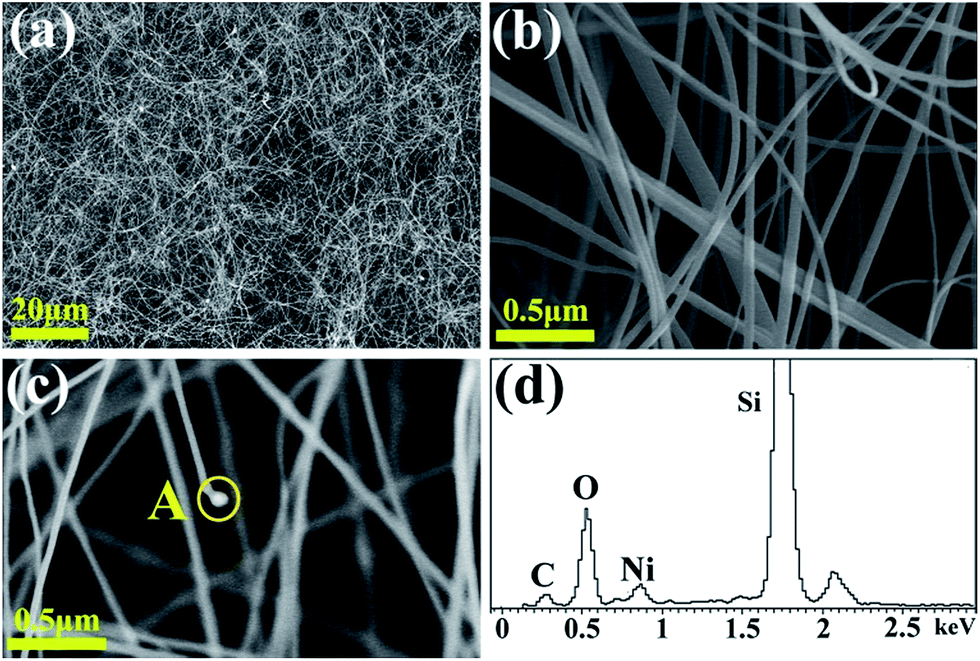 | ||
| Fig. 6 (a) Low magnification and (b) and (c) high magnification FESEM images of the nanowires synthesized with catalyst, (d) EDS pattern of the droplet recorded from the marked area A in (c). | ||
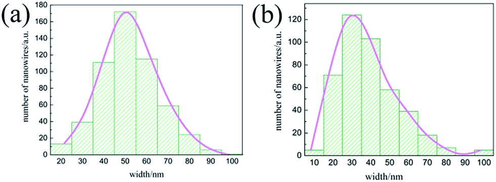 | ||
| Fig. 7 (a) Size distribution of as-grown nanowires without catalyst, and (b) with catalyst. | ||
According to the thermodynamic calculations, Ni(NO3)2 on the graphite felt will decompose and form nano-NiO particles at 260 °C (as shown in reaction (9)).35 Later, the nano-Ni particles will form by the reaction (10) between nano-NiO particles and graphite felt, which provide catalytically active sites for the formation of nuclei and the growth of nanowires.
| 2Ni(NO3)2 → 2NiO + 4NO2 + O2 | (9) |
| 2NiO + C → 2Ni + CO2 | (10) |
The existence of catalyst will affect the application of SiC nanowires. So, when put the as-grown SiC nanowires with catalyst in application, the metallic catalyst must be removed. It involves complicated equipment and processes.
Conclusions
In summary, SiC/SiO2 nanowires were synthesized by a facile chemical vapour deposition method at 1300 °C using Si and SiO2 mixture powders as raw materials without any catalysts. The as-obtained nanowires were composed of a crystalline SiC core and an amorphous SiO2 shell. The average diameter of the nanowires was about 50 nm and their length was about hundreds of microns. The SiC-core nanowires grew along [111] direction and stacking faults were existed along their growth direction. The as-synthesized nanowires without using catalysts were grown via VS mechanism. Due to the stacking faults and the presence of the amorphous SiO2 layer, the SiC/SiO2 nanowires showed a blue-shift PL spectrum. The SiC/SiO2 core–shell nanowires as reported in this research have potential application in future blue-green emitting devices.Acknowledgements
This work was supported by the National Natural Science Foundation of China (Grant No. 51272241, 51472222 and 51372232).Notes and references
- K. Zekentes and K. Rogdakis, J. Phys. D: Appl. Phys., 2011, 44, 133001 CrossRef.
- R. A. Andrievski, Sci. Adv. Mater., 2009, 22, 1–20 CAS.
- Y. N. Xia, P. D. Yang, Y. G. Sun, Y. Y. Wu, B. Mayers, B. Gates, Y. D. Yin, F. Kim and H. Q. Yan, Adv. Mater., 2003, 15, 353–389 CrossRef CAS.
- L. D. Zhang, G. W. Meng and F. Phillipp, Mater. Sci. Eng., A, 2000, A286, 34–38 CrossRef CAS.
- G. Z. Shen and D. Chen, Nanotechnology, 2010, 4, 20–31 CAS.
- W. M. Zhou, L. J. Yan, Y. Wang and Y. F. Zhang, Appl. Phys. Lett., 2006, 89, 1–3 Search PubMed.
- Z. G. Wang, J. B. Li, F. Gao and W. J. Weber, Acta Mater., 2010, 58, 1963–1971 CrossRef CAS.
- W. John, I. V. Lyver and B.-B. Estela, J. Comput. Theor. Nanosci., 2011, 8, 529–534 CrossRef.
- Y. G. Sun and Y. N. Xia, Adv. Mater., 2002, 14, 833–837 CrossRef CAS.
- S. Kodambaka, J. Tersoff, M. C. Reuter and F. M. Ross, Science, 2007, 316, 729–732 CrossRef CAS PubMed.
- S. Z. Deng, Z. S. Wu, J. Zhou and N. S. Xu, Chem. Phys. Lett., 2002, 356, 511–514 CrossRef CAS.
- Y. F. Zhang, Y. H. Tang, N. Wang, D. P. Yu, C. S. Lee, I. Bello and S. T. Lee, Appl. Phys. Lett., 1998, 72, 1835–1837 CrossRef CAS.
- J. J. Chen, Y. Pan and R. B. Wu, Rare Met. Mater. Eng., 2010, 39(2), 90 Search PubMed.
- R. B. Wu, G. Y. Yang, Y. Pan and J. J. Chen, J. Phys. D: Appl. Phys., 2007, A86, 271–274 Search PubMed.
- K. F. Cai, A. X. Zhang, J. L. Yin, H. F. Wang and X. H. Yuan, J. Phys. D: Appl. Phys., 2008, A91, 579–584 Search PubMed.
- J. J. Chen, R. B. Wu and Y. Pan, J. Nanosci. Nanotechnol., 2010, 10, 1–6 CrossRef.
- A. Meng, M. Zhang, W. D. Gao, S. B. Sun and Z. J. Li, Nanoscale Res. Lett., 2011, 6, 34–41 CrossRef PubMed.
- D. H. Feng, T. Q. Jia, X. X. Li, Z. Z. Xu, J. Chen, S. Z. Deng, Z. S. Wu and N. S. Xu, Solid State Commun., 2003, 128, 295–297 CrossRef CAS.
- Q. G. Fu, H. J. Li, X. H. Shi, K. Z. Li, J. Wei and Z. B. Hu, Mater. Chem. Phys., 2006, 100, 108–111 CrossRef CAS.
- C. H. Liang, G. W. Meng, L. D. Zhang, Y. C. Wu and Z. Cui, Chem. Phys. Lett., 2000, 329, 323–328 CrossRef CAS.
- J. X. Dai, J. J. Sha, Z. F. Zhang, Y. C. Wang and W. Krenkel, Ceram. Int., 2015, 41, 9637–9641 CrossRef CAS.
- H. T. Liu, Z. H. Huang, M. H. Fang, Y. G. Liu and X. W. Wu, J. Cryst. Growth, 2015, 419, 20–24 CrossRef CAS.
- H. T. Liu, Z. H. Huang, J. T. Huang, M. H. Fang, Y. G. Liu and X. W. Wu, J. Mater. Chem. C, 2014, 2, 7761–7767 RSC.
- J. J. Chen, Q. Shi and W. H. Tang, Mater. Chem. Phys., 2011, 126, 655–659 CrossRef CAS.
- W. Khongwong, M. Imai, K. Yoshida and T. Yano, J. Ceram. Soc. Jpn., 2009, 117, 439–444 CrossRef CAS.
- E. Zhang, Y. H. Tang, Y. Zhang and G. Chi, Phys. E, 2009, 41, 657 Search PubMed.
- X. G. Luo, W. H. Ma, Y. Zhou, D. C. Liu, B. Yang and Y. N. Dai, Nanoscale Res. Lett., 2010, 5, 252–256 CrossRef CAS PubMed.
- L. M. Ghiringhelli, C. Valeriani, J. H. Los, E. J. Meijer, A. Fasolino and D. Frenkel, Mol. Phys., 2008, 106, 2011–2038 CrossRef CAS.
- K. Chen, Z. H. Huang, J. T. Huang, M. H. Fang, Y. G. Liu, H. P. Ji and L. Yin, Ceram. Int., 2013, 39, 1959 Search PubMed.
- K. Senthil and K. Yong, Mater. Chem. Phys., 2008, 112, 88–93 CrossRef CAS.
- B. Park, Y. Ryu and K. Yong, Surf. Rev. Lett., 2004, 11, 372–378 Search PubMed.
- S. Z. Deng, Z. B. Li, W. L. Wang, N. S. Xu, J. Zhou, X. G. Zheng, H. T. Xu, J. Chen and J. C. She, Appl. Phys. Lett., 2006, 89, 23118–23120 CrossRef.
- D. Sharma, A. Motayed, S. Krylyuk, Q. L. Li and A. V. Davydov, IEEE Trans. Electron Devices, 2013, 60, 4206–4212 CrossRef CAS.
- J. T. Huang, S. W. Zhang, Z. H. Huang, Y. G. Liu and M. H. Fang, CrystEngComm, 2013, 15, 785–790 RSC.
- J. T. Huang, Y. G. Liu, Z. H. Huang, M. H. Fang, S. W. Zhang, W. Xie, J. Z. Yang, S. F. Huang and Y. G. Xu, Cryst. Growth Des., 2013, 13, 10–14 CAS.
Footnote |
| † Electronic supplementary information (ESI) available. See DOI: 10.1039/c5ra27139h |
| This journal is © The Royal Society of Chemistry 2016 |