
Pressure induced semiconductor–metal phase transition in GaAs: experimental and theoretical approaches†
Jia Wangab,
Baojia Wu*ab,
Guozhao Zhangab,
Lianhua Tiana,
Guangrui Gua and
Chunxiao Gao*b
aDepartment of Physics, College of Science, Yanbian University, Yanji, Jilin 133002, China. E-mail: jbwu@ybu.edu.cn
bState Key Lab for Superhard Materials, Institute of Atomic and Molecular Physics, Jilin University, Changchun, Jilin 130012, China. E-mail: cc060109@qq.com
First published on 8th January 2016
Abstract
Gallium arsenide (GaAs) exhibits outstanding electron transport properties that are useful for many electronics industries. High pressure is a powerful way to induce dramatic electrical conductivity changes in materials. Herein, we investigated the electrical transport properties of GaAs under high pressure up to 25.0 GPa by in situ alternating-current (AC) impedance spectroscopy measurements, temperature dependent electrical resistivity measurements, and first-principles calculations. The experimental results showed that GaAs undergoes a semiconductor to metal transition at approximately 12.0 GPa, which corresponds to the pressure-induced phase transition of GaAs from a zinc-blende to a Cmcm structure. In addition, the dramatic changes in electrical transport parameters, such as the bulk resistance, relaxation frequency, and resistivity, were observed at 12.0 GPa. First-principles calculations show that the energy bands crossed the Fermi level for the Cmcm phase, at the same time electronic localization began to decreases at 12.0 GPa, leading to the metallization of GaAs.
1. Introduction
Gallium arsenide (GaAs) is one of the most valuable semiconductors in the electronics industry. GaAs exhibits outstanding electron transport properties and during the previous decades it has been widely used as a substrate material.1–6 Due to its high conversion efficiencies and high mobility, GaAs can be also applied in solar cells and high-speed digital circuits, respectively.7–10High pressure is a powerful way to induce dramatic changes in the crystal structures and electronic structures of materials.11,12 High pressure be able to continuously tune the crystal and electronic structures away from the pristine state to a wide array of application, and then affect application characters.13 Moreover, high pressure has the ability to alter completely the electrical conductivity of some materials such as semiconductor to metal transitions.13–16 This type of behaviour which pressure-modulated crystal structure and electrical properties of some materials provides a new developing platform for electronic industries.
GaAs exists in a zinc-blende (zb) form and has a direct band gap energy of 1.42 eV under ambient pressures.17 GaAs has received great interest under extremely compressed conditions with considerable experimental and theoretical research.18–32 Experimentally, the pressure-induced structural transformation has already been fully explored with different methods, such as electrical resistance measurements,18 synchrotron radiation X-ray diffraction,19–22,24–28 Raman scattering,22,23 X-ray absorption,22 electron microscopy,22 and thermopower S (Seebeck effect).30 High pressure experimental studies on GaAs clearly demonstrated the pressure-induced phase transition of GaAs from a zinc-blende (zb) to a Cmcm structure at P = 11.2–17.3 GPa.12 Interestingly, recent first-principles calculations have predicted the Cmcm phase is metallic because the energy bands cross the Fermi level during the phase transition.29,31 Despite theoretical studies suggesting metallization of GaAs, no experimental evidence for such a transition has been proven to date. Therefore, exploring the metallic state of GaAs under high pressure by an experimental approach has become important to investigate.
In this study, we conducted the test method for high pressure in situ temperature-dependent electrical resistivity measurements to verify whether the semiconductor–metal transition of GaAs can occur in structural phase transition. Combined with the experimental results, first-principles calculations were used to obtain a further understanding of the structural phase transition and the electrical conductivity in GaAs under compression. Furthermore, high pressure in situ impedance spectroscopy results will demonstrate the effects of bulk and grain boundaries on the electrical transport properties of GaAs.
2. Experimental
The GaAs sample (99.999% purity) was purchased from Alfa Aesar Co. The initial structure of the sample was the zinc blende (space group F![[4 with combining macron]](https://www.rsc.org/images/entities/char_0034_0304.gif) 3m). A diamond anvil cell (DAC) with a 300 μm diameter anvil culet was used to generate high pressure. T-301 stainless steel was pre-indented to 60 μm as a gasket. A 5 μm ruby was used as a pressure calibrator by using its R1 line wavelength shift. No pressure medium was used to prevent the introduction of additional resistance. The sample thickness under pressure was determined by a micrometer, and then the deformation of the diamond anvils was considered.33 Molybdenum thin film electrodes were fabricated on the diamond anvil used as electric measurement probes. The van der Pauw configuration was used in the high-pressure in situ AC impedance spectroscopy measurements and temperature dependent electrical resistivity measurements.34
3m). A diamond anvil cell (DAC) with a 300 μm diameter anvil culet was used to generate high pressure. T-301 stainless steel was pre-indented to 60 μm as a gasket. A 5 μm ruby was used as a pressure calibrator by using its R1 line wavelength shift. No pressure medium was used to prevent the introduction of additional resistance. The sample thickness under pressure was determined by a micrometer, and then the deformation of the diamond anvils was considered.33 Molybdenum thin film electrodes were fabricated on the diamond anvil used as electric measurement probes. The van der Pauw configuration was used in the high-pressure in situ AC impedance spectroscopy measurements and temperature dependent electrical resistivity measurements.34
The AC impedance spectra of GaAs were obtained by a Solartron 1260 impedance analyzer equipped with a Solartron 1296 dielectric interface. The frequency ranged from 0.1 Hz to 10 MHz, and the AC voltage amplitude was 1 V. The electrical resistivity was determined by the van der Pauw method using the equation as follows:35
| exp(−πR1d/ρ) + exp(−πR2d/ρ) = 1, | (1) |
The first-principles calculations for GaAs were performed on the basis of density functional theory in the CASTEP code.36 The electron–ion interaction was described by Vanderbilt-type ultrasoft pseudopotentials.37 The exchange and correlation terms were described using a generalized gradient approximation (GGA) in the Perdew–Burke–Ernzerhof (PBZ) scheme.38 Structural optimizations were performed using the Broyden–Fletcher–Goldfarb–Shanno minimization algorithm provided in this code.39 Integration in the Brillouin zone was performed using special k points generated by 6 × 6 × 6 and 7 × 7 × 7 mesh parameter grids for the zb and Cmcm phases, respectively. The one-electron valence state was expanded on the basis of a plane wave with a 528 eV cutoff energy. An ultrafine computational accuracy was used. The configurations of Ga and As are 3d10 4s1 4p1 and 4s2 4p3, respectively.
3. Results and discussion
3.1 High-pressure AC impedance spectroscopy
AC complex impedance spectroscopy is a powerful tool for separating the bulk and grain boundary effects of materials.40,41 Grain boundaries are usually undesired in some practical applications on account of this making a negative effect on the electrical transport of some materials.42,43 AC impedance spectra of GaAs in the complex plane and the frequency of imaginary part are shown in Fig. 1(a) to (d). Fig. 1(a) and (b) shows only one semicircle in the complex plane at each pressure. There is only one relaxation peak at each pressure in Fig. 1(c) and (d). The observed semicircle and relaxation peak represent the bulk transport property.44 The undesired grain boundary effect was not observed in GaAs under compression. When the applied pressure reached 13.0 GPa [Fig. 1(b)], the semicircle transforms into a quarter of a circular arc because the resistance of the sample was too small to overcome the measured resistance range. Under compression, from normal pressure to 13.0 GPa, the bulk effect dominates the electrical transport properties of GaAs and applying no pressure-modulates the grain boundary effect. | ||
| Fig. 1 (a and b) The impedance spectra as a Nyquist diagram and (c and d) the imaginary parts of impedance vs. frequency for GaAs at different pressures, respectively. Inset in (b) impedance spectra as a Nyquist diagram for GaAs at 13.0 GPa. | ||
The total resistance is the intercept of the semicircle with the real axis, as shown in Fig. 2(a). The relaxation frequency is the value that imaginary part versus frequency, as shown in Fig. 2(b). As the pressure increased to below 11.9 GPa, the resistance value gradually decreased and the relaxation peaks gradually moved to a higher frequency. Pressure-induced band-gap shrinkage can lead to increased conductivity.45 The resistance sharply decreased by two orders of magnitude and the relaxation peaks move to significantly higher frequencies when the pressure ranged from 11.9 GPa to 13.0 GPa [Fig. 2(a) and (b)]. The abrupt change in resistance and relaxation frequency at approximately 12.0 GPa resulted from the structural phase transition from the zb phase to the Cmcm phase, as reported in the Raman scattering experiment of Besson et al.22 The structure phase transition realigns the atomic position, leads to abrupt change in resistance and polarization mode, which affects the vibrational frequency of the atoms in the GaAs sample. In addition, because the resistance decreases by two orders of magnitude within one pressure range, we speculated that the metallization could be happening during the structural phase transition.
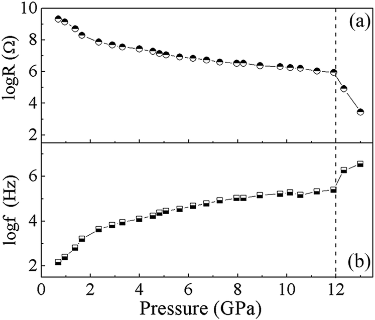 | ||
| Fig. 2 The pressure dependence of resistance and relaxation frequency of GaAs. | ||
3.2 In situ electrical resistivity measurements under high pressure
The AC impedance spectroscopy measurements overcame the measurable range of the instrumentation when the applied pressure reached 13.0 GPa. We carried out high-pressure in situ electrical resistivity measurements for up to 25.0 GPa at room temperature. As shown in Fig. 3, the electrical resistivity of GaAs was very high and exceeds the upper measurable limit of the instrument from ambient pressure to 4.0 GPa. From 4.0 GPa to 12.0 GPa, the electrical resistivity of GaAs gradually decreased with increasing pressure. From 12.0 GPa to 13.0 GPa, the electrical resistivity sharply decreased by three orders of magnitude. The sudden change in the electrical resistivity was related to a first-order structural transition. Earlier high pressure XRD experiments have confirmed that GaAs undergoes a structural phase transition at approximately this pressure.22 From 13.0 GPa to 25.0 GPa, the electrical resistivity continues to decrease with increasing pressure. During the decompression process, the resistivity returns from the low-value state at 25 GPa to a high-value state, as the pressure returns to its ambient conditions. This phenomenon is attributed to the reversible phase-transition from the Cmcm phase to the zb phase. In fact, reversible phase transitions reported in most XRD and Raman studies showed that the diffraction peaks and spectral characteristics could return to their original states after the pressure is released.22 However, the physical properties of the sample exhibit a relaxation feature called hysteresis as pressure is released, such as the hysteresis of the XRD patterns, Raman spectroscopy and resistance, observed in this work. Combining AC complex impedance spectroscopy measurements with in situ electrical resistivity measurements, the decreasing magnitudes in the bulk resistance and resistivity were observed in the structural phase transition. According to the metallization recently predicted by theoretical calculations, we further speculated that Cmcm phase is metallic in the experiment.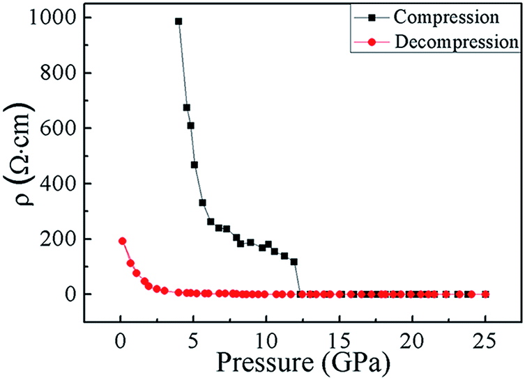 | ||
| Fig. 3 Pressure depedence of electrical resistivity of GaAs at room temperature. | ||
3.3 Temperature dependence of resistivity measurements
To uncover whether the Cmcm structure is metallic, the temperature dependence of the electrical resistivity measurements was investigated at different pressures. Ten pressure points (five from the zb phase and five from the Cmcm phase) were selected. The temperature dependence of the electrical resistivity in GaAs was plotted in an Arrhenius format at 10 pressure points in Fig. 4(a). The results show that below 12.0 GPa, the electrical resistivity of GaAs with a zb structure decreased with increasing temperature. This trend indicates the presence of a semiconducting state in zb GaAs. Above 12.0 GPa, the electrical resistivity showed a positive relationship with temperature. This finding indicated that Cmcm GaAs is metallic. From 11.2 GPa to 16.7 GPa, the temperature did not significantly vary with the resistivity, as show in Fig. 4(b). The results show that the completion of the semiconductor to metal transformation needs a period of pressure. The temperature dependence of the electrical resistivity measurements revealed that metallization has occurred during the structural phase transition, and that a six orders of magnitude tenability for the resistivity has existed in the compression from the semiconducting to metallic state. | ||
| Fig. 4 Temperature-dependence of electrical resistivity of GaAs (a) temperature–resistivity curves plotted in an Arrhenius format at several pressures. (b) Temperature–pressure–resistivity contour map. | ||
3.4 First-principles calculations
First-principles calculations were performed to study the micro-mechanism of the metallization in GaAs under high pressure. The changing enthalpy vs. pressure relationships of the zb and Cmcm phases are shown in Fig. 5. The enthalpy of the zb and Cmcm phases intersected at 12 GPa. The enthalpy value of the zb phase was relatively stable below 12 GPa, whereas the enthalpy of Cmcm was relatively stable after 12 GPa. This phenomenon explains why the pressure-induced phase transition occurred at 12 GPa from the zb phase to the Cmcm phase. These results are consistent with the high-pressure in situ AC impedance spectroscopy and electrical resistivity results. Therefore, the drastic changes in the bulk resistance, relaxation frequency, and electrical resistivity around 12 GPa can be attributed the zb–Cmcm structure phase transition in GaAs. | ||
| Fig. 5 The change enthalpy vs. pressure relationships of the zb and Cmcm phases of GaAs. | ||
The band structure calculation was carried out at two representative pressures to study the pressure-induced band structure variations of GaAs. As shown in Fig. 6(a), both the bottom of the conduction band and the top of the valence band are located at the same G point. The band gap of the zb structure at 6 GPa was approximately 0.82 eV. This result indicated that the zb structure of GaAs was a direct band gap semiconductor and the value of band gap was decreased under compression. For the Cmcm phase, as shown in Fig. 6(b), the band gap across the Fermi level indicated that the Cmcm phase was metallic. Pressure-induced band-gap shrinkage and large movements of the orbits towards the EF occurred. By further increasing the pressure, the metallic band structure was ultimately obtained.
 | ||
| Fig. 6 Calculated band structure of (a) the zb phase at 6 GPa and (b) the Cmcm phase at 20 GPa. | ||
The difference charge density of the zb and the Cmcm phases are shown in Fig. 7. In the zb phase, the Ga atom and As atoms form a covalent bond at the site with the maximum charge density that exhibits strong electron localization. As the pressure was increased, the bonding charge densities increased because of the decreasing interatomic distances. As a result, the electric charge aggregation increased with increasing pressure. In the Cmcm phase, the density of the free electrons around the Ga and As atoms increased and the electron localization decreased obviously compared with those in the zb phase. These results can be explained by the decrease in the covalent properties and the increase in metallic properties as the pressure was increased. When the applied pressure exceeded 15 GPa, the Cmcm phase exhibited a metallic state.
 | ||
| Fig. 7 Calculated difference charge density for the zb phase (1 GPa and 10 GPa) and the Cmcm phase (15 GPa and 25 GPa). | ||
4. Conclusions
In summary, we have carried out in situ AC impedance spectroscopy, temperature dependent electrical resistivity measurements, and first-principles calculations in GaAs under high pressure. The pressure dependent AC impedance spectroscopy indicates that both the bulk resistance and relaxation frequency exhibited abrupt changes at 12.0 GPa, which corresponded to the pressure-induced phase transition of GaAs from a zinc-blende to a Cmcm structure. The temperature dependent electrical resistivity measurements show that GaAs undergoes a transition from semiconductor to metal at approximately 12.0 GPa. This method confirms that the metallic state has underwent a first-order structural transition and reveals the tenability of six orders of magnitude for resistivity ranging from the semiconducting to metallic state. First-principles calculations also indicated the micro-mechanism of pressure-induced metallization in GaAs and the pressure-induced conduction bands crossed the Fermi level for the Cmcm phase. The results of the difference charge density calculations indicated that the electronic localization decreased, whereas the metallic properties increased, with increasing pressure, in the Cmcm phase.Acknowledgements
This study was supported by the National Basic Research Program of China (Grant No. 2011CB808204), the National Natural Science Foundation of China (Grant No. 11164031, 51362028, 51272224, 11374121, 11404133, 11304114, and 51273079), and the Program of Science and Technology Development Plan of Jilin Provience (Grant No. 20140520105JH).References
- J. A. del Alamo, Nature, 2011, 479, 317 CrossRef CAS PubMed.
- S. H. Zhang, W. Xu, S. M. Badalyan and F. M. Peeters, Phys. Rev. B: Condens. Matter Mater. Phys., 2013, 87, 075443 CrossRef.
- R. Kumar, P. Mukhopadhyay, A. Bag, S. K. Jana, A. Chakraborty, S. Das, M. K. Mahata and D. Biswas, Appl. Surf. Sci., 2015, 324, 304 CrossRef CAS.
- T. Sekihara, R. Masutomi and T. Okamoto, Phys. Rev. Lett., 2013, 111, 057005 CrossRef PubMed.
- M. Sacchi, M. Marangolo, C. Spezzani, L. Coelho, R. Breitwieser, J. Milano and V. H. Etgens, Phys. Rev. B: Condens. Matter Mater. Phys., 2008, 77, 165317 CrossRef.
- F. L. Gao, L. Wen, J. L. Li, Y. F. Guan, S. G. Zhang and G. Q. Li, CrystEngComm, 2014, 16, 10774 RSC.
- W. Choi, C. Z. Kim, C. S. Kim, W. Heo, T. Joo, S. Y. Ryu, H. Kim, H. Kim, H. K. Kang and S. Jo, Adv. Energy Mater., 2014, 4, 1400589 Search PubMed.
- F. Dimroth, M. Grave, P. Beutel, U. Fiedeler, C. Karcher, T. N. D. Tibbits, E. Oliva, G. Siefer, M. Schachtner, A. Wekkeli, A. W. Bett, R. Krause, M. Piccin, N. Blanc, C. Drazek, E. Guiot, B. Ghyselen, T. Salvetat, A. Tauzin, T. Signamarcheix, A. Dobrich, T. Hannappel and K. Schwarzburg, Progress in Photovoltaics: Research and Applications, 2014, 22, 277 CrossRef CAS.
- K. Lee, J. Lee, B. A. Mazor and S. R. Forrest, Light: Sci. Appl., 2015, 4, e288 CrossRef CAS.
- Y. Ju, T. Kobayashi and H. Soyama, Microsyst. Technol., 2008, 14, 1021 CrossRef CAS.
- A. Jayaraman, Rev. Mod. Phys., 1983, 55, 65 CrossRef CAS.
- A. Mujica, A. Rubio, A. Munoz and R. J. Needs, Rev. Mod. Phys., 2003, 75, 863 CrossRef CAS.
- Z. Zhao, H. J. Zhang, H. T. Yuan, S. B. Wang, Y. Lin, Q. S. Zeng, G. Xu, Z. X. Liu, G. K. Solanki, K. D. Patel, Y. Cui, H. Y. Hwang and W. L. Mao, Nat. Commun., 2015, 6, 7312 CrossRef CAS PubMed.
- A. P. Nayak, Z. Yuan, B. X. Cao, J. liu, J. J. Wu, S. T. Moran, T. S. Li, D. J. Akinwande, C. Q. Jin and J. F. Lin, ACS Nano, 2015, 9, 9117 CrossRef CAS PubMed.
- E. Arcangeletti, L. Baldassarre, D. D. Castro, S. Lupi, L. Malavasi, C. Marini, A. Perucchi and P. Postorino, Phys. Rev. Lett., 2007, 98, 196406 CrossRef CAS PubMed.
- A. Segura, V. Panchal, J. F. S. Royo, V. M. Borras, V. M. Sanjose, P. R. Hernandez, A. Munoz, E. P. Gonzalez, F. J. Manjon and J. Gonzalez, Phys. Rev. B: Condens. Matter Mater. Phys., 2012, 85, 195139 CrossRef.
- A. M. Cowley and S. M. Sze, J. Appl. Phys., 1965, 36, 3212 CrossRef CAS.
- S. Minomura and H. G. Drickamer, J. Phys. Chem. Solids, 1962, 23, 451 CrossRef CAS.
- S. Yu, I. Spain and E. Skelton, Solid State Commun., 1978, 25, 49 CrossRef CAS.
- M. Baublitz and A. Ruoff, J. Appl. Phys., 1982, 53, 6179 CrossRef CAS.
- S. T. Weir, Y. K. Vohra, C. A. Vanderborgh and A. L. Ruoff, Phys. Rev. B: Condens. Matter Mater. Phys., 1989, 39, 1280 CrossRef CAS.
- J. M. Besson, J. P. Itié, A. Polian, G. Weill, J. Mansot and J. Gonzalez, Phys. Rev. B: Condens. Matter Mater. Phys., 1991, 44, 4214 CrossRef CAS.
- U. D. Venkateswaran, L. J. Cui and B. A. Weinstein, Phys. Rev. B: Condens. Matter Mater. Phys., 1991, 43, 1875 CrossRef CAS.
- R. J. Nelmes, M. I. Mcmahon, N. G. Wright, D. R. Allan, H. Liu and J. S. Loveday, J. Phys. Chem. Solids, 1995, 56, 539 CrossRef CAS.
- M. I. McMahon and R. J. Nelmes, Phys. Status Solidi B, 1996, 198, 389 CrossRef CAS.
- M. I. McMahon and R. J. Nelmes, Phys. Rev. Lett., 1997, 78, 3697 CrossRef CAS.
- M. I. Mcmahon, R. J. Nelmes, D. R. Allan, S. A. Belmonte and T. Bovornratanaraks, Phys. Rev. Lett., 1998, 80, 5564 CrossRef CAS.
- M. I. Mcmahon and R. J. Nelmes, Phys. Rev. Lett., 2005, 95, 215505 CrossRef CAS PubMed.
- H. Arabi, A. Pourghazi, F. Ahmadian and Z. Nourbakhsh, Phys. B, 2006, 373, 16 CrossRef CAS.
- S. V. Ovsyannikov and V. V. Shchennikov, J. Phys.: Condens. Matter, 2006, 18, 551 CrossRef.
- D. C. Gupta and S. Kulshrestha, J. Phys.: Condens. Matter, 2008, 20, 255204 CrossRef.
- P. Pluengphon, T. Bovornratanaraks, S. Vannarat and U. Pinsook, Solid State Commun., 2014, 195, 26 CrossRef.
- M. Li, C. X. Gao, G. Peng, C. Y. He, A. M. Hao and X. W. Huang, Rev. Sci. Instrum., 2007, 78, 075106 CrossRef PubMed.
- M. Li, C. X. Gao, Y. Z. Ma, D. J. Wang, Y. C. Li and J. Liu, Appl. Phys. Lett., 2007, 90, 113507 CrossRef.
- P. M. Hemenger, Rev. Sci. Instrum., 1973, 44, 698 CrossRef CAS.
- M. D. Segall, P. J. D. Lindan, M. J. Probert, C. J. Pickard, P. J. Hasnip and S. J. Clark, J. Phys.: Condens. Matter, 2002, 14, 2717 CrossRef CAS.
- D. Vanderbilt, Phys. Rev. B: Condens. Matter Mater. Phys., 1990, 41, 7892 CrossRef.
- J. P. Perdew, K. Burke and M. Ernzerhof, Phys. Rev. Lett., 1996, 77, 3865 CrossRef CAS PubMed.
- T. H. Fischer and J. Almlof, J. Phys. Chem., 1992, 96, 9768 CrossRef CAS.
- Y. Li, Y. H. Han, Y. Z. Ma, P. W. Zhu, X. Wang and C. X. Gao, Europhys. Lett., 2012, 98, 66006 CrossRef.
- D. M. Zhang, Y. S. Zhang, Y. Gao, Y. H. Han, C. X. Gao and Y. Z. Ma, J. Appl. Phys., 2012, 111, 063718 CrossRef.
- J. H. Achon, S. Berg, C. Kloc and B. Batlogg, Science, 2000, 287, 1022 CrossRef.
- J. Y. Yan, F. Ke, C. L. Liu, Q. L. Wang, J. K. Zhang, L. Wang, G. Peng, Y. H. Han, Y. Z. Ma and C. X. Gao, Phys. Chem. Chem. Phys., 2015, 17, 26277 RSC.
- Q. L. Wang, Y. H. Han, C. L. Liu, Y. Z. Ma, W. B. Ren and C. X. Gao, Appl. Phys. Lett., 2012, 100, 172905 CrossRef.
- C. L. Liu, Y. M. Sui, W. B. Ren, B. H. Ma, Y. Li and N. N. Su, Inorg. Chem., 2012, 51, 7001 CrossRef CAS PubMed.
Footnote |
| † Electronic supplementary information (ESI) available. See DOI: 10.1039/c5ra25013g |
| This journal is © The Royal Society of Chemistry 2016 |