DOI:
10.1039/C5RA23694K
(Paper)
RSC Adv., 2016,
6, 7582-7590
High-definition conductive silver patterns on polyimide film via an ion exchange plating method†
Received
10th November 2015
, Accepted 10th January 2016
First published on 14th January 2016
Abstract
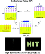
In this work, we developed a new ion exchange plating (IEP) method that is different to traditional electrochemical plating or electroless plating techniques. A variety of silver patterns were prepared by using the IEP technique as demonstrated in this work. The key factors to the definition and the conductive performance of silver patterns were systematically studied. Mechanisms of the formation of the conductive silver patterns was studied as well. A new model was established for elucidating the deposition process. Importantly, using this IEP method coupled with mask technology, double-sided interconnected conductive silver patterns on polyimide substrates were successfully fabricated with high definition. This new technology will provide a unique capability to fabricate double-sided or multi-sided interconnection for next generation printed circuit board (PCB).
1. Introduction
Conductive patterns have many applications including integrated circuits (IC), radio frequency identification (RFID) electronic tags, and molded interconnect devices (MID). Owing to these important applications, more attention has been drawn recently in research to the preparation of high-definition conductive patterns. Of all metals, silver has the highest conductivity, leading to the proposal of many methods of fabricating silver patterns on flexible substrates in the past few years. At first, scientists chose to prepare silver patterns by direct printing silver nanoparticle ink on flexible substrates followed by a sintering process at high temperature.1–5 This method has many disadvantages including the use of high sintering temperature and instability of silver nanoparticle inks. The high sintering temperature is required to remove the dispersants and the high boiling point solvents used for adding into inks to stabilize Ag nanoparticles and to reduce the coffee ring effect, respectively. To obtain sufficiently high conductivity, dispersants and solvents must be decomposed or volatilized. To reduce the sintering temperature, many researchers attempted to use different sintering methods, such as intense pulse light,6 microwave,7 argon plasma,8 and opposite charge effect,9 however, the instability of silver nanoparticles is still a big problem. Novel silver precursor ink methods have been proposed in order to resolve this silver nanoparticle instability. Silver precursor inks include two types: organic silver precursor inks and inorganic silver precursor inks. Organic silver precursor inks can be further divided into three categories: the first, organic silver decomposition ink, can be directly decomposed to a conductive silver layer at a specific temperature.10,11 The second, fractional reduction method, uses organic silver precursor ink pre-printed on the substrate followed by silver reduction via exposure to reduction conditions.12 Lastly the third, direct inspired reduction ink, uses a potential reductant added to the ink which inspires to a true reductant at particular temperatures13–15 or by laser radiation.16
Inorganic silver precursor inks mainly consist of silver nitrate or silver oxide as a precursor. Silver nitrate decomposes at about 440 °C and silver ions must be reduced with a reductant. Inorganic silver precursor inks can be divided into two types, similar to the first two types mentioned with regard to organic precursor inks: fractional reduction method and direct inspired reduction ink. The fractional reduction method uses silver ion ink pre-printed on substrates, which is then reduced to silver by exposure to reduction conditions17 or printing reductant ink.18,19 Direct inspired reduction ink includes a reductant precursor that is added to the ink, which decomposes to a true reductant such as aldehyde at the proper temperature.20,21
In the past decades, a novel ion exchange self-metallization method was employed to fabricate conductive silver coatings on polyimide substrates.22–27 The amide bond of polyimide film can be hydrolyzed to carboxyl potassium compounds in strong alkali solution. Silver ions are doped into the alkali modification layer by ion exchange process. Finally, the conductive silver layer is obtained by reduction process (reduction action, migration and assembly). A typical reduction procedure includes chemical reductants, UV light, or high heat treatment. Owing to the excellent binding force between the silver layer and polyimide film, many researchers have begun preparing a variety of silver patterns on the polymer film.28–30 As for the studied methods, a mask is necessary to ensure the definition of conductive patterns when a variety of conductive patterns are prepared on polyimide films via ion exchange and electroless plating processes.31 Several problems that arise from this mask process, however, are difficult to solve. These difficulties include stringent requirements for the mask, reversible and non-residual removal of mask, and potential micro crack damages to polyimide substrates. All of these issues are caused by strong corrosion modification and penetration of the alkali solution.
Considering the aforementioned problems, we were inspired by the idea that ion exchange resins can be regenerated (Fig. 1a). Arising from this, we report on a novel method to obtain conductive silver coatings on polyimide films by continuous ion exchange processes. The new method named “Ion Exchange Plating (IEP)” is totally different from the traditional electrochemical plating or electroless plating techniques. In addition, compared with the traditional ion exchange self-metallization method (Fig. 1b), IEP method has many advantages such as only minor damage to polyimide film, low requirements for the mask (when used in the preparation of silver patterns), and the silver layer thickness is not dependent on the degree of alkali modification, but instead on IEP repetitions under particular conditions. The principle scheme of this method is shown in Fig. 1c. It can be found that the ion exchange process's smooth progression is due to the introduction of a neutralizing regeneration process unlike the traditional ion exchange self-metallization method.
 |
| Fig. 1 (a) A scheme of ion exchange resins. (b) A scheme of fabricating one conductive silver layer via a traditional ion exchange self-metallization method. (c) A scheme of repeatable IEP method. | |
2. Experimental details
2.1 Fabricating silver patterns by an IEP method via mask technology
A typical preparation procedure of fabricating conducive silver pattern onto a polyimide film was presented in Fig. 1c. In order to prepare alkali modification solution, glycerin was first mixed with deionized water. Then potassium hydroxide (KOH) was added into the glycerin solution and the beaker was sealed immediately. The mixture was stirred until potassium hydroxide was completely dissolved and cool down to room temperature. On the other hand, the double-sided polyimide film (TORAY Dupont, Kapton 500H, 50 × 50 × 0.125 mm3) was rinsed with ethyl alcohol in order to remove the possible grease. The bright side of polyimide film was covered with a polyvinyl chloride (PVC) hollow mask (covered with no residual polyacrylate pressure-sensitive adhesive and variety of patterns). Then the polyimide film was immersed in the prepared alkali modification solution at room temperature for 1 min followed by rinsing with deionized water. After peeling off the PVC mask, the pretreatment of polyimide with the alkali modification pattern was completed. The above treated polyimide film was immersed in 0.4 M silver nitrate solution at room temperature for 1 min, and then rinsed with deionized water. Next, the polyimide film was immersed in 0.25 M ascorbic acid in order to reduce adsorbed Ag+ to metallic Ag. The solution pH was adjusted between 3 and 4 by using ammonium hydroxide aqueous solution (volume ratio 1
:
1). Finally, a neutralizing regeneration process (abbreviation N) was carried out. In particular, the treated polyimide film was immersed in 50 g L−1 potassium hydrogen phosphate solution at room temperature for 1 min, and was washed with deionized water. Above procedure was repeated until the conductivity of silver pattern layer met the requirements. After the reduction process, the entire IEP process was finished. Then the above polyimide film was rinsed with deionized water and blow-dried by the cold wind. As a result, the polyimide film with the silver pattern was prepared completely.
2.2 Physical characterization
During the preparation of conductive silver patterns, scanning electron microscopy (SEM) was used to monitor their morphology changes. In addition, elemental contents in the patterns were measured by using coupled energy dispersive spectrometer (EDS). The line width of the silver pattern was measured using metallographic microscope. The thickness of the silver layer of the silver pattern was determined using the CMI900 & 950 X-ray Fluorescence Spectrometer (Oxford Instruments). Definition of the silver patterns was observed by using USB electronic microscope. Conductivity of the silver pattern was tested with the ST2258C multifunction digital four-probe tester (Suzhou Jingge Electronic Co., Ltd).
3. Results and discussion
3.1 Fabricating silver patterns on polyimide film
Feasibility of an IEP method via mask technology to fabricate silver patterns on polyimide films was first investigated. Before the neutralizing regeneration process (Fig. S1a†), elemental contents determined by EDS indicated a silver pattern is composed of C (5.93 wt%), N (15.66 wt%), O (41.45 wt%), and Ag (36.95 wt%). However, after the neutralizing regeneration process (Fig. S1b†), it is composed of C (6.95 wt%), N (9.01 wt%), O (46.41 wt%), K (9.81 wt%) and Ag (27.82 wt%). The detected potassium confirms that an alkali modification layer on the polyimide film can be regenerated after the neutralizing regeneration process. Regeneration of the modification layer indicates that it is feasible using the IEP method with repeatable steps to fabricate silver patterns to obtain sufficient thickness on polyimide films.
Furthermore, circular silver patterns on polyimide film were fabricated with 15 repetitions by using the IEP method (Fig. 2a). We also prepared a circular silver pattern by using only one repetition as a comparison (Fig. 2b). Their surface morphology, adhesion, conductivity and definition of the obtained circular silver pattern were also characterized.
 |
| Fig. 2 Silver patterns on polyimide film fabricated by using the IEP method. Digital photographs of circular silver pattern (diameter of the circle pattern: 3 cm) prepared by (a) 15 IEP repetitions and (b) one IEP repetition with conditions: immersing time t(I) = 120 min and reducing time t(R) = 15 min. (c) and (d) Microscope images for (a) and (b), respectively. (e) and (f) The corresponding definition images for (a) and (b). (g) Digital photograph of (a) crossed by Cross-Cut Tester (2 mm space) and after the 3M 600 tape test. (h) Microscope image of (g). Scale bars in (a)–(e) and their inserts and (h) are 0.5 and 0.123 mm, respectively. | |
The appearance of circular silver pattern prepared by 15 IEP repetitions is white color (Fig. 2a), while the one prepared by only one IEP repetition is a light blue-white color (Fig. 2b). The thickness of the pattern layer prepared by 15 IEP repetitions is 0.23 μm that is much thicker than the 0.02 μm of the one obtained by one repetition. Moreover, the circular silver pattern layer prepared by 15 IEP repetitions has a more uniform surface (Fig. 2c), smaller sheet resistance value 0.281 Ω cm−2 (Table S1†), and smaller resistivity value 6.46 μΩ cm (the conductivity is 24.61% of the bulk silver value), relative to the one by one repletion. The results of definition measurements (Fig. 2e and f) show that sufficient definition of silver patterns can be fabricated by the IEP method. The results of a cross-cut test and the 3M 600 tape test (Fig. 2g), along with the clear scratch observation test (Fig. 2h) indicated a good adhesion between the silver layer and polyimide film.
3.2 Factors to affect silver patterns
After confirming the feasibility, we further studied key factors that control the eventual properties of the silver patterns (e.g., including definition and conductivity) fabricated by the IEP method. We first studied the definition of silver patterns as functions of the mass ratios of glycerin to deionized water, and the time of alkali modification process t(A). With increasing mass ratios of glycerin to deionized water, the permeability and causticity of the alkali modification solution become weaker and the definition of silver patterns become higher (Fig. 3). However, further increasing amounts of glycerin leads to poor dissolving performance of potassium hydroxide, thereby resulting in a reduced definition. Therefore, the optimal mass ratio of glycerin to deionized water was determined to be 1
:
1.
 |
| Fig. 3 The influence of the mass ratios of glycerin to deionized water on the definition of circular (Φ 3 cm) silver pattern on polyimide film prepared (note: IEP repetitions n = 5, rt × 1 min). The definition images of circular (Φ 3 cm) silver pattern observed by USB electronic microscope (a) mass (glycerin) : mass (water) = 1 : 3. (b) Mass (glycerin) : mass (water) = 1 : 2. (c) Mass (glycerin) : mass (water) = 1 : 1. (d) Mass (glycerin) : mass (water) = 2 : 1. Scale bars in (a)–(d) and their inserts are 0.5 and 0.123 mm, respectively. | |
Another factor that affects definition of silver patterns is the time of alkali modification process t(A). With increasing time of the alkali modification process t(A), permeability and causticity of the alkali modification solution are enhanced, and therefore the definition of obtained silver patterns becomes deteriorated (Fig. 4). In addition, we systematically investigated the conductivity of silver patterns as functions of alkali modification process t(A), the mass ratio of glycerin to deionized water, IEP repetitions (n), and the concentration of AgNO3, C6H8O6, and K2HPO4. As listed in Table S1,† longer alkali modification time and more IEP repetitions result in thicker silver pattern layers and smaller sheet resistance. However, it should be noted that smaller sheet resistance does not mean lower resistivity. There is a close relationship between thickness and conductivity of silver pattern layers. To get good electrical conductivity, a certain thickness of the silver layer is necessary. Thus, we further determined the correlations between these factors (i.e. alkali modification process t(A), the mass proportion of glycerin to water, IEP repetitions and the concentration of AgNO3, C6H8O6, and K2HPO4) and thickness of silver pattern layers.
 |
| Fig. 4 The influence of the time of alkali modification process t(A) on the definition of circular (Φ 3 cm) silver pattern on polyimide film prepared by an IEP method via mask technology (note: IEP repetitions n = 5). The definition images of circular (Φ 3 cm) silver patterns observed by USB electronic microscope. (a) t(A) = 1 min. (b) t(A) = 2 min. (c) t(A) = 3 min. (d) t(A) = 4 min. (e) t(A) = 5 min. Scale bars in (a)–(e) and their inserts are 0.5 and 0.123 mm, respectively. | |
As is shown in Fig. 5a, under the same alkali modification condition with an increasing mass ratios of glycerin to deionized water, permeability and causticity of the alkali modification solution becomes weaker, leading to a drop in the hydrolysis degree of polyimide film. This decreases silver ion exchange capacity, leading to a significant drop in the thickness of the silver pattern layer. Similarly, with increasing the time of the alkali modification process t(A), stronger permeability and causticity of the alkali modification lead to a rise of hydrolysis degree of polyimide films, thereby increasing the silver ion exchange capacity as well as the thickness of the silver pattern layers (Fig. 5b). Significantly different from the above results, a wide variety of concentration of AgNO3 (0.4–1.0 M), C6H8O6 (0.25–1.0 M), and K2HPO4 (50–200 g L−1) have insignificant effects on the thickness.
 |
| Fig. 5 The influence of the mass proportion of glycerin to deionized water (IEP repetitions n = 5) (a), the time of alkali modification process t(A) (repetitions n = 5) (b) and IEP repetitions n (c) on the thickness d of circular (Φ 3 cm) silver pattern layer on polyimide film prepared by an IEP method via mask technology (note: alkali modification condition: mass (KOH) : mass (H2O) : mass (C3H8O3) = 1 : 1 : 1). (d) The influence of IEP repetitions n on the sheet resistance R□ and resistivity ρ of circle (Φ 3 cm) silver pattern layer on polyimide film prepared by an IEP method via mask technology. | |
IEP repetitions (n) is a vital factor in ion exchange plating method. Generally, a continuous supply of metal ions on the surface of the substrate is necessary for continuous growth of the metal coating for both the electrochemical plating and electroless plating methods. The ion exchange plating method relies on IEP repetitions to attain a continuous supply of silver ions and the continuous growth of a silver coating under certain conditions. It can be seen that the thickness of the silver pattern layer shows a linear growth with an increase in IEP repetitions (Fig. 5c). Here we define the plating rate V of the ion exchange plating as follows:
where Δ
d is the thickness increment of silver pattern layer, and Δ
n is the increment of IEP repetitions. According to the above description, the plating rate
V of the ion exchange plating is approximately equal to the slope of the linear fit line 0.01371 μm per times (
Fig. 5c).
Conductivity of the silver pattern layer as a function of IEP repetitions was investigated. With an increase of IEP repetitions, the silver pattern layers transited from insulating, partly conductive, completely conductive but not uniformly conductive, to uniformly conductive (Fig. 5d). When IEP repetitions is less than three, the layer is very thin and insulating. Increasing IEP repetitions to 11, the obtained silver layer becomes partly conductive. When IEP repetitions reaches 13, the layer appears completely conductive, but the conductivity is not uniform. Until IEP repetitions is more than 15, the layer eventually achieves even conductivity. Further increasing IEP repetitions lead to insignificant change of conductivity. The sheet resistance of the silver pattern layer with sufficient thickness is in the range of 0.2 to 0.5 Ω cm−2. The resistivity of silver pattern can reach 6–10 μΩ cm, which is 15.9–26.5% of the bulk silver value at 20 °C.
Furthermore, with an increase in IEP repetitions, the color of the silver pattern layer gradually changes from light blue-white to white (Fig. S2†) and the surface of silver pattern layer grows more uniform. This can be attributed to the silver pattern layer becoming thicker with more IEP repetitions. The above results are confirmed by SEM images (Fig. S3†). In addition, larger particles of silver are getting more numerous (Fig. S3†). The emergence of large particles makes the surface profile of the silver pattern layer rougher with more IEP repetitions. The roughness of silver layers were studied using AFM, showing an increasing trend with more IEP repetitions (from n = 15 to 23) (Fig. 6).
 |
| Fig. 6 AFM three-dimensional height images of circular silver patterns fabricated by the IEP method via mask technology under different IEP repetitions n. (a) n = 15, (b) n = 17, (c) n = 19, (d) n = 21, and (e) n = 23. (f) Surface roughness Ra of silver patterns as function of repetition n. | |
To further explain the formation process of the conductive silver patterns fabricated by the IEP method, a possible model was proposed as shown in Fig. 7. At first, potassium carboxylate groups are generated on polyimide films via a hydrolysis process under alkali modification solution. Then, silver ions can be adsorbed on polyimide films via an ion exchange process. A thin silver layer can then be prepared on polyimide films via a reduction process (including reduction, migration and assembly stages). After the reduction process, carboxyl groups are generated at the surface of polyimide films. After one IPE repetition, only little silver particles formed on the surface. Conductivity is very poor. Subsequently, repeating IEP procedures, including alkaline modification, adsorption of silver ions, reduction, and neutralizing regeneration, lead to more deposited silver particles, thereby resulting in gradually increased thickness and conductivity. Eventually, polyimide films are completely covered by uniform silver layers.
 |
| Fig. 7 A possible model for the formation process of a silver pattern layer fabricated by IEP method on polyimide film. | |
3.3 Preparation of high-definition silver patterns on polyimide film
In order to further demonstrate the practical application of the newly develop IEP method to prepare silver patterns, we fabricated a variety of silver patterns on polyimide films using the IEP method via mask technology including 0.5 mm line pattern (Fig. 8a), 1.0 mm line pattern (Fig. 8b) and “HIT” characters pattern (Fig. 8c). The silver line width measurement of 0.5 mm and 1.0 mm line patterns by metallographic microscope is 507.34 μm (Fig. 8e) and 947.20 μm (Fig. 8f) respectively. They show a small deviation (The relative error is 1.47% and −5.28% respectively) compared with the theoretical value. There is potential in preparing a much higher definition and conductive silver patterns in the future. Moreover, we successfully prepared a double-sided interconnected circular silver pattern (Fig. 8d). The resistance was measured at 116.3 Ω, revealing that a double-sided circular silver pattern achieved conductive interconnection in one step for the first time by a small hole (Φ 1.0 mm) in the center of silver pattern. This manufacturing process is completely different from the traditional preparation process of interconnected PCB, whose pattern metallization process and hole metallization process are separated.
 |
| Fig. 8 Preparation of a variety of silver patterns on polyimide films by the develop IEP method via mask technology. The digital photograph of 0.5 mm (a) and 1.0 mm (b) line silver patterns (ion exchange plating repetitions n = 15). (c) The digital photograph of the “HIT” silver pattern (note: ion exchange plating repetitions n = 21, HIT is the abbreviation of Harbin Institute of Technology). (d) The digital photograph of the conductivity test of double-sided interconnection conductive circular (Φ 3 cm) silver pattern on a polyimide film (note: an interconnection small hole (Φ 1 mm) lies in the center of silver pattern, ion exchange plating repetitions n = 30). (e) and (f) The silver line width measurement of (a) and (b) by metallographic microscope, respectively. | |
4. Conclusions
In this work, we developed a novel ion exchange plating (IEP) method to prepare high-definition and conductive silver patterns on polyimide films potentially for printed circuit board (PCB) fabrication. Compared to traditional ion exchange self-metallization methods, the IEP leads to negligible damage to polyimide films and doesn't require masks during film fabrication. Importantly, thickness of the silver layers is not dependent on the degree of alkali modification, and only controlled by the repetition times of ion exchange plating process. By using the IEP to prepare silver patterns, higher mass ratio of glycerin to deionized water and less alkali modification time can improve the definition of the silver patterns. Thickness of silver pattern layers show a linear growth with an increase of IEP repetitions. The optimal IEP repetitions were determined in terms of achieving sufficient conductivity and definition. The key factors to film quality was systematically studied to maximize silver coverage and minimize the agglomerated silver particles. Finally, we successfully fabricated various silver patterns on polyimide films by the IEP method. Resistivity of the fabricated silver patterns can be reduced to 6–10 μΩ cm, which is 15.9–26.5% of the bulk silver value at 20 °C. Importantly, for the first time, a double-sided interconnected conductive silver pattern on polyimide substrate was fabricated by the IEP method couple with mask technology via one step. The new method to prepare double-sided or multi-sided interconnection will lay a solid foundation for PCB application. In addition, the IEP method may be applied in preparing other metals or metal oxides on polyimide films or other potential substrates for a variety of applications.
Acknowledgements
We acknowledge financial support by Highnic Group in Guangdong. G. W. thank the financial support from start-up fund from the University at Buffalo, SUNY.
References
- S. H. Yoon, J. H. Lee, P. C. Lee, J. D. Nam, H. C. Jung, Y. S. Oh, T. S. Kim and Y. K. Lee, Macromol. Res., 2009, 17, 568 CrossRef CAS.
- K. J. Lee, B. H. Jun, T. H. Kim and J. Joung, Nanotechnology, 2006, 17, 2424 CrossRef CAS.
- B. Y. Ahn, D. J. Lorang and J. A. Lewis, Nanoscale, 2011, 3, 2700 RSC.
- S. Jeong, H. C. Song, W. W. Lee, Y. Choi and B. H. Ryu, J. Appl. Phys., 2010, 108, 102805–102811 CrossRef.
- I. K. Shim, Y. I. Lee, K. J. Lee and J. Joung, Mater. Chem. Phys., 2008, 110, 316 CrossRef CAS.
- J. S. Kang, J. Ryu, H. S. Kim and H. T. Hahn, J. Electron. Mater., 2011, 40, 2268 CrossRef CAS.
- B. J. Perelaer, M. Klokkenburg, C. E. Hendriks and U. S. Schubert, Adv. Mater., 2009, 21, 4830 CrossRef.
- I. Reinhold, C. E. Hendriks, R. Eckardt, J. M. Kranenburg, J. Perelaer, R. R. Baumannbd and U. S. Schubert, J. Mater. Chem., 2009, 19, 3384 RSC.
- S. Magdassi, M. Grouchko, O. Berezin and A. Kamyshny, ACS Nano, 2010, 4, 1943 CrossRef CAS.
- X. Nie, H. Wang and J. Zou, Appl. Surf. Sci., 2012, 261, 554 CrossRef CAS.
- S. F. Jahn, T. Blaudeck, R. R. Baumann, A. Jakob, P. Ecorchard, T. Rüffer, H. Lang and P. Schmidt, Chem. Mater., 2010, 22, 3067 CrossRef CAS.
- J. J. P. Valeton, K. Hermans, C. W. M. Bastiaansen, D. J. Broer, J. Perelaer, U. S. Schubert, G. P. Crawford and P. J. Smith, J. Mater. Chem., 2010, 20, 543 RSC.
- Y. Wu, Y. Li and B. S. Ong, J. Am. Chem. Soc., 2007, 129, 1862 CrossRef CAS.
- Y. Li, Y. Wu and B. S. Ong, J. Am. Chem. Soc., 2005, 127, 3266 CrossRef CAS.
- S. B. Walker and J. A. Lewis, J. Am. Chem. Soc., 2012, 134, 1419 CrossRef CAS.
- Y. K. Liu and M.-T. Lee, ACS Appl. Mater. Interfaces, 2014, 6, 14576 CAS.
- J. T. Wu, S. L. C. Hsu, M. H. Tsai and W. S. Hwang, Thin Solid Films, 2009, 517, 5913 CrossRef CAS.
- S. M. Bidoki, D. M. Lewis, M. Clark, A. Vakorov, P. A. Millner and D. McGorman, J. Micromech. Microeng., 2007, 17, 967 CrossRef CAS.
- Z. K. Kao, Y. H. Hung and Y. C. Liao, J. Mater. Chem., 2011, 21, 18799 RSC.
- Y. L. Tai, Z. G. Yang and Z. D. Li, Appl. Surf. Sci., 2011, 257, 7096 CrossRef CAS.
- S. P. Chen, Z. K. Kao, J. L. Lin and Y. C. Liao, ACS Appl. Mater. Interfaces, 2012, 4, 7064 CAS.
- Y. Shang, G. Cui, H. Ma, S. Qi, D. Wu, W. Guo and Z. Wu, J. Macromol. Sci., 2014, 1, 46 Search PubMed.
- F. Y. Shen, S. E. Huang and W. P. Dow, ECS Electrochem. Lett., 2013, 2, D45 CrossRef CAS.
- G. Cui, S. Qi, X. Wang, G. Tian, G. Sun, W. Liu, X. Yan, D. Wu, Z. Wu and L. Zhang, J. Phys. Chem. B, 2012, 116, 12349 CrossRef CAS.
- Z. Wu, D. Wu, S. Qi, T. Zhang and R. Jin, Thin Solid Films, 2005, 493, 179 CrossRef CAS.
- Z. Wu, D. Wu, W. Yang and R. Jin, J. Mater. Chem., 2006, 16, 310 RSC.
- S. Yang, D. Wu, S. Qi, G. Cui, R. Jin and Z. Wu, J. Phys. Chem. B, 2009, 113, 9694 CrossRef CAS.
- S. Gout, J. Coulm, D. Léonard and F. Bessueille, Appl. Surf. Sci., 2014, 307, 716 CrossRef CAS.
- F. Yang, W. Su, L. Yao, L. Liang, Y. Liu, S. Yu and Y. Zhu, Adv. Mater. Res., 2012, 510, 176 CrossRef CAS.
- K. Akamatsu, S. Ikeda and H. Nawafune, Langmuir, 2003, 19, 10366 CrossRef CAS.
- K. Akamatsu, S. Ikeda, H. Nawafune and H. Yanagimoto, J. Am. Chem. Soc., 2004, 126, 10822 CrossRef CAS.
Footnote |
† Electronic supplementary information (ESI) available. See DOI: 10.1039/c5ra23694k |
|
This journal is © The Royal Society of Chemistry 2016 |
Click here to see how this site uses Cookies. View our privacy policy here.