Yao Liang*a,
Yingying Wangb,
Jianan Wanga,
Sumei Wua,
Dayong Jiang*c and
Jiabiao Lian*d
aSchool of Materials Science and Engineering, Dalian Jiaotong University, Dalian 116028, P. R. China. E-mail: yliang0625@hotmail.com
bDepartment of Optoelectronic Science, Harbin Institute of Technology at Weihai, Weihai 264209, P. R. China
cSchool of Materials Science and Engineering, Changchun University of Science and Technology, Changchun 130022, P. R. China. E-mail: dayongjiangcust@126.com
dSchool of Civil and Environmental Engineering, College of Engineering, Nanyang Technological University, Singapore 639798. E-mail: jblian@ntu.edu.sg
First published on 18th January 2016
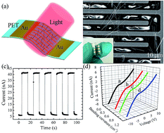
Antimony selenide (Sb2Se3) has many potential applications in photoelectric devices, thermoelectric cooling devices and electrochemical devices etc. It also has many special properties due to its layered structure. A simple hydrothermal method was used to synthesize Sb2Se3 nanowires of high crystalline quality. (Sb4Se6)n layers are parallel to the growth direction of the Sb2Se3 nanowire. A single Sb2Se3 nanowire demonstrated a remarkable response to 635 nm light at 10 V with the responsivity and external quantum efficiency of 360 A W−1 and 7.0 × 10⁴%, respectively. The rise/fall time was 0.4/1.3 s. Flexible photodetectors were fabricated by dispersing a large number of Sb2Se3 nanowires onto the Au interdigitated electrodes on PET substrates, which showed a fast response speed with the rise/fall time as low as 13/20 ms and excellent flexibility. The high-performance of the photodetectors may be partially attributed to the layered structure. Generally, high-yield Sb2Se3 nanowires synthesized by the hydrothermal method are promising candidates for high-performance flexible photodetectors.
Sb2Se3 as an important member of group V and VI binary semiconductors can be used to fabricate electric, photoelectric, thermoelectric cooling and electrochemical devices, which is attributed to its direct and narrow band-gap, high environmental stability and Seebeck coefficient.24–27 It is a highly anisotropic semiconductor with the layered structure parallel to the [001] (c-axis) direction.28,29 Sb2Se3 has demonstrated promise in solar cells due to its layered structure.30 Thus, it can be believed that single-crystalline Sb2Se3 nanowires have many special properties owing to the carrier and photon confinement in the layered structure.29 Sb2Se3 nanowires have been synthesized by hydrothermal/solvothermal routes or microwave-assisted methods.25,28,31 However, the studies on the application of Sb2Se3 nanowires are limited. Zhai et al. utilized individual Sb2Se3 nanowire to fabricate a photodetector with a marked response to 600 nm visible-light.29 Choi et al. also studied the response of single Sb2Se3 nanowire to 655 nm visible-light.27 The photodetectors based on Sb2Se3 nanowire films displayed a remarkable response to white light.31 The results above indicate that Sb2Se3 nanowires have bright prospects for visible-light photodetectors. However, these Sb2Se3 nanowire based photodetectors were fabricated on the rigid SiO2/Si substrates, which do not meet the need for portable devices. To the best of our knowledge, the application of Sb2Se3 nanowires in flexible electronics has not been explored. Thus, it is necessary to further investigate the electrical transport and photoelectric properties of single Sb2Se3 nanowire, assemble a large number of nanowires into the flexible photodetector, and finally characterize its performances. It is desirable to achieve high-performance flexible photodetectors via a simple method.
In this work, a simple hydrothermal method was used to synthesize single-crystalline Sb2Se3 nanowires in high yields. Single Sb2Se3 nanowire field-effect transistors (FETs) demonstrated the p-type transport characteristic of single nanowire. They were also utilized to investigate the photoelectric properties of single Sb2Se3 nanowire. A single Sb2Se3 nanowire showed a remarkable response to 635 nm light at 10 V with high responsivity (360 A W−1) and short response time (0.4/1.3 s). Flexible photodetectors with fast response speed (13/20 ms) and excellent flexibility were made by dispersing a large number of Sb2Se3 nanowires onto the Au interdigitated electrodes on PET substrates, revealing the potential application of Sb2Se3 nanowires in flexible photodetectors.
![]() | ||
Fig. 1 (a) SEM image of Sb2Se3 nanowires. (b) Crystalline structure of Sb2Se3. (Sb4Se6)n layers are parallel to the growth direction of Sb2Se3 nanowire. |
Single Sb2Se3 nanowire based FETs were fabricated to investigate the electrical transport properties of single nanowire. The upper inset in Fig. 2 is a schematic illustration of the FET. The lower inset in Fig. 2 is an SEM image of the FET, showing that two Cr/Au electrodes are attached onto a single Sb2Se3 nanowire. The FET's channel is about 6.4 μm in length and 135 nm in width. Fig. 2 displays IDS versus VDS curves at a different back-gated voltage (VG) varying from −30 V to 30 V. The nonlinear IDS–VDS curves indicate Schottky contacts between the nanowire and Cr/Au electrodes. The conductance of the Sb2Se3 nanowire decreases with the increasing of positive VG, proving that the nanowire is p-type. Compared to bulk materials, nanomaterials could have different electrical transport properties due to large surface-to-volume ratio. Sb2Se3 in bulk is well-known p-type semiconductor.25 Here, Sb2Se3 nanowires have the same conductivity type as the bulk.
![]() | ||
Fig. 2 IDS–VDS characteristics of a single Sb2Se3 nanowire FET at different VG. Insets are a schematic illustration and an SEM image of the FET, respectively. |
In the previous report,25 the band-gap energy of Sb2Se3 nanowires have been examined by UV-vis absorption spectra and derived to range from 1.16 to 1.17 eV, indicating that Sb2Se3 nanowires can detect all visible-light in principle. The photoelectric properties of the Sb2Se3 nanowire, shown in the lower inset of Fig. 2, were investigated. The inset of Fig. 3a is a schematic illustration of photoelectric measurement. Fig. 3a demonstrates I–V curves of the nanowire in the dark and under the 635 nm light illumination of different power densities. The photocurrent (Ilight–Idark) increases with the increasing of the power density of incident light at a fixed bias. It is clear that the nanowire is sensitive to 635 nm light. The energy of incident photons is 1.95 eV, which is larger than the band-gap energy of Sb2Se3. Under the illumination of 635 nm light, electron–hole pairs are generated in the Sb2Se3 nanowire, which leads to the increase of the conductivity of the nanowire.
Responsivity (Rλ = Iph/(PS), where Iph is photocurrent, P is the power density of incident light and S is the effective illuminated area) and external quantum efficiency (EQE = hcRλ/(eλ), where λ is the wavelength, h is Planck's constant, e is the electronic charge and c is the speed of light) are important parameters representing the sensitivity of photodetector.32 The single Sb2Se3 nanowire photodetector has Rλ and EQE as high as 360 A W−1 and 7.0 × 10⁴% respectively at a bias of 10 V (the calculation is shown in the ESI†). The Rλ is higher than that (Rλ = 8.0 A W−1) of the single Sb2Se3 nanowire photodetector reported by Zhai et al. and comparable to that (Rλ = 560 A W−1) reported by Choi et al.27,29 It can be concluded that Sb2Se3 nanowires synthesized by this hydrothermal method have a potential application in visible-light detection. The higher Rλ and EQE are attributed to excellent crystalline quality of Sb2Se3 nanowires.14 Fig. 3b shows the dependences of the photocurrent on the power density of incident light at 1 V, 5 V and 10 V, respectively. Usually, the relationship can be described by a power law (Iph = A × PC, Iph is photocurrent, P is power density, A and C are constants). The solid lines are the best fitting results. The C values correspond to 0.82, 0.59 and 0.57, respectively. They are smaller than 1, indicating that multiple trap states exist in a single Sb2Se3 nanowire and lead to a complex process of electron–hole generation, trapping and recombination under the illumination.1,3 The time responses of the single Sb2Se3 nanowire were recorded by periodically turning 635 nm light on and off, as shown in Fig. 3c and d. It is noted that the photocurrents are stable and reversible. The rise time (fall time) is defined as the time interval for the response to rise (decay) from 10–90% (90–10%) of photocurrent. The single Sb2Se3 nanowire photodetector has the rise/fall time of 2.2/3.7 s, 0.6/3.1 s and 0.4/1.3 s at a bias of 1 V, 5 V and 10 V, respectively. These response times are comparable to those of Sb2Se3 nanowire photodetectors and other nanowire photodetectors.29,33,34 There are rare dangling bonds on the surface of Sb2Se3 nanowires due to the layered structure.30 Less dangling bonds indicate less surface states in the surface region. It has been known that a long response time is due to the existence of a large amount of surface states, and vice versa.35 Thus, the fast response to 635 nm light should be attributed to the layered structure of Sb2Se3. It is also observed that the response time can be shorted by increasing the bias. Increasing the bias can enhance the strength of the electric field in the nanowire, which could accelerate the trapping and releasing process of carriers and finally lead to a fast response. In addition, the fall time is longer than the rise time at a fixed bias.
The fabrication process of single nanowire based photodetectors is complex, expensive and time consuming. Moreover, single nanowire's photocurrent is too small to be detected. Thus, single nanowire based photodetectors are hard to be used widely in daily life. Recently, flexible electronics have attracted more attention due to the demand for portable devices. In this work, a large number of Sb2Se3 nanowires were randomly dispersed onto the Au interdigitated electrodes on PET substrates to fabricate flexible photodetectors. Fig. 4a is a schematic illustration of flexible photodetector. Because the Au interdigitated electrodes are made on the flexible PET substrate, as shown in the inset of Fig. 4b, the photodetector could possess excellent flexibility. A flexible photodetector was characterized by SEM (Fig. 4b). It is observed that many Sb2Se3 nanowires are on the interdigitated electrodes and connect adjacent electrodes. As the PET substrate is insulating, there are some bright areas between electrodes induced by the charging effect. Fig. 4c reveals I–V characteristics of a multiple Sb2Se3 nanowires based photodetector (D1) in the dark and under the illumination of 635 nm light with different power densities. The photocurrent increases by increasing the power density of incident light at a fixed bias, and their relationships are shown in Fig. 4d. Similarly, the relationships still can be described by the power law (Iph = A × PC). C values are taken by fitting corresponding data and are 0.79, 0.72 and 0.80 at a bias of 1 V, 5 V and 10 V, respectively. These values are different from those of the single Sb2Se3 nanowire photodetector, which is attributed to the difference of electron–hole generation, trapping and recombination processes in two kinds of photodetectors. It is possible that interfaces among nanowires lead to this difference. It is desired to achieve photodetectors of a higher C value.32 Compared to the single Sb2Se3 nanowire based photodetector, the multiple nanowires based photodetector has higher C values at 5 V, 10 V and a similar value at 1 V.
Fig. 5a shows I–V curves of another flexible Sb2Se3 nanowires based photodetector (D2) in the dark and under the illumination of 31 mW cm−2 635 nm light. Compared to D1, the D2 displays a tenfold increase in photocurrent and dark current under the same conditions due to the increasing of the number of nanowires on the interdigitated electrodes. The time responses of the D2 were recorded (Fig. 5b and c). With 635 nm light on and off, the D2 shows “on-state” and “off-state” repeatedly. It has a fast response to the light and a reproducible and stable photocurrent. Fig. 5c illustrates an on–off cycle of the D2 under the illumination of 31 mW cm−2 635 nm light at a bias of 10 V with 1 ms time resolution. According to this on–off cycle, it can be deduced that the rise/fall time is 17/20 ms. In order to confirm the fast response of this kind of flexible photodetectors, the performances of other photodetectors also were characterized. One of them is shown in Fig. S3.† The rise/fall time of the DS1 is 13/20 ms and close to 17/20 ms obtained above. Fig. S3c† reveals the ability of the DS1 to detect 635 nm light with an on–off frequency up to 230 Hz. The response time is an important parameter determining the capability of photodetector to follow a fast changing light. The response speed of our flexible photodetectors is faster than those of many flexible photodetectors.15,20,22 Thus, our synthesized Sb2Se3 nanowires are promising to fabricate high-speed flexible photodetectors. Compared to the single nanowire photodetector, multiple Sb2Se3 nanowires photodetectors have a faster response speed. Fig. S4† shows that increasing the number of nanowires in the photodetector can improve response speed. The mechanism is still unknown and will be further studied. It is possible that the faster response speed of multiple nanowires photodetector is attributed to the rapid recombination of photogenerated electron–hole pairs at the interfaces between nanowires.11 Except for 635 nm light, flexible Sb2Se3 nanowires photodetectors can be used to detect visible-light of other wavelength, such as 405 nm violet light. Fig. S5† illustrates the response of a flexible photodetector to 405 nm light, which is similar to the response to 635 nm light.
As multiple Sb2Se3 nanowires photodetectors were fabricated on PET substrates, they should possess a significant property, i.e. flexibility. It is necessary to know the influence of bending on the electrical properties of flexible photodetectors. Fig. 6a–d are photographs recording different bending states of a flexible photodetector during I–V tests. The corresponding I–V curves are displayed in Fig. 6e. It is noted that the bending curvature has not an obvious influence on I–V characteristic of the flexible photodetector. The relationships between the current through the photodetector and the bending curvature are shown in Fig. 6f. The current slightly decreases with the increasing of bending curvature, which is reasonable since the electrode interspacing should slightly increase with the bending curvature and finally has an influence on the current.1 However, the currents of the photodetector with different bending curvatures keep at 6.0 ± 0.2 nA. The change of current is negligible and acceptable, indicating the excellent flexibility of this kind of photodetector. Fig. 6g demonstrates I–V curves of the photodetector without bending (blue solid line) and after 1000 cycles of bending (red circles). It can be observed that I–V characteristic of the photodetector is hardly affected even after 1000 cycles of bending. All results confirm that dispersing Sb2Se3 nanowires onto the Au interdigitated electrodes is suitable for making flexible photodetectors with high-performance. Since (Sb4Se6)n layers are parallel to the growth direction of Sb2Se3 nanowire, the nanowires could have large bending strain compliance. Thus, excellent flexibility should be also related to the layered structure.
Our results are compared with other Sb2Se3 nanostructure based photodetectors reported so far (Table 1). In this work, the single Sb2Se3 nanowire shows an excellent light-detection performance with high responsivity and fast time response. Sb2Se3 nanowires can be assembled into a flexible photodetector with faster time response and excellent flexibility by a simple method. This work first reveals that high-yield Sb2Se3 nanowires are promising candidates for flexible photodetectors.
Photodetectors | Response time (s) | Responsivity (A W−1) | EQE (%) | Flexibility | Reference |
---|---|---|---|---|---|
Single Sb2Se3 nanowire | 560 | 1.06 × 10⁵ | No | 27 | |
Single Sb2Se3 nanowire | <0.3 s | 8.0 | 1650 | No | 29 |
Multiple Sb2Se3 nanowires | 0.2/1.2 s | No | 31 | ||
Single Sb2Se3 nanowire | 0.4/1.3 s | 360 | 7.0 × 10⁴ | No | This work |
Multiple Sb2Se3 nanowires | 13/20 ms | Yes | This work |
Footnote |
† Electronic supplementary information (ESI) available. See DOI: 10.1039/c5ra23542a |
This journal is © The Royal Society of Chemistry 2016 |