Organic thin film transistors with novel photosensitive polyurethane as dielectric layer

Yao Lia, He Wangb, Xuehui Zhanga, Qiong Zhanga, Xuesong Wanga, Danfeng Caoa, Zuosen Shia, Donghang Yan*b and Zhanchen Cui*a
aKey Lab of Supramolecular Structure & Materials, College of Chemistry, Jilin University, Changchun 130012, PR China. E-mail: cuizc@jlu.edu.cn
bState Key Laboratory of Polymer Physics and Chemistry, Changchun Institute of Applied Chemistry, Chinese Academy of Sciences, Changchun 130012, PR China

Received 2nd November 2015 , Accepted 17th December 2015

First published on 21st December 2015


Abstract

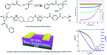
In this paper, we report the design, synthesis, and dielectric properties of a novel photosensitive polyurethane dielectric film used in organic thin-film transistors (OTFTs). The novel photosensitive polyurethane dielectric film is readily fabricated by spin coating followed by curing under UV light. The film exhibits excellent insulating properties, smooth surface, and excellent photosensitive properties. The bottom-gate top-contact para-sexiphenyl (p-6P)/vanadyl-phthalocyanine (VOPc) OTFTs with photosensitive polyurethane films as the dielectric layer exhibit excellent performance with a mobility of 0.13 cm2 V−1 s−1, on/off ratio of 104 and ultralow leakage.


1. Introduction

Unlike conventional inorganic technology, organic thin-film transistor (OTFT)-based electronics performing simple operations provide unique qualities, including low cost, large-area coverage, and low processing temperatures.1–6 In particular, para-sexiphenyl (p-6P)/vanadyl-phthalocyanine (VOPc) OTFTs have attracted considerable attention and have already demonstrated their potential toward organic electronic applications.7–10 However, the critical issue that limits the performance of p-6P/VOPc OTFTs is their large leakage current. The dielectric layer, as an important part of OTFTs, can effectively influence the leakage current and performance of these devices. One approach to reducing leakage current is the use of novel organic/inorganic dielectric materials as dielectric layer.11–14 Furthermore, OTFTs have been fabricated by using high-density self-assembled monolayers (SAMs) dielectric films as dielectric layer.15–18 These methods exhibit excellent insulating properties and have been successfully used in OTFTs. However, current pathways for the integration of these layers into large-area coating processes are inapplicable.

For large-area electronic applications, various solution-processable materials are chosen as dielectric layer because these materials can be formed simply via spin-coating, casting, or printing at room temperature.19–22 However, compared with traditional materials, insulation of solution-processable materials is not enough. Therefore, increasing the insulation of solution-processable materials is a major challenge in fabricating large-area electronic applications of OTFTs. As reported, leakage current can be minimized due to the reduced free volume in the dielectric layer, which guaranteed a more active cross-linking reaction.23–25 For cross-linking materials, one major choice is to employ an organic cross-linker in the solution-processable materials solution. Another effective solution is the use of a novel polymer structure with cross-linked group, such as epoxy group.26 The resulting OTFTs with these dielectric layer function at a low leakage current. However, the critical issue that limits application of these methods is a high temperature processes and a shorter storage time. Therefore, it is necessary to develop cross-linking and low-temperature processable solution-processable materials as dielectric layers.

Photosensitive solution-processable materials are considered viable alternative materials that can simplify procedures and reduce the manufacturing costs of large-area electronic applications.27,28 In particular, solution-processable polyurethane has attracted considerable attention, due to high tensile strength, excellent abrasion resistance and good mechanical properties.29 In this work, to afford a photosensitive cross-linking solution-processable material, we design and synthesis a novel monomer that contained hydroxy and olefin groups. This monomer can copolymerize with 4,4′-methylenebis(cyclohexyl isocyanate), and 2,2-bis butyl cinnamoylate (hydroxymethyl) to obtain a solution-processable photosensitive polyurethane. These monomers can provide a more flexible structure to improve film-forming property of polyurethane. In this polyurethane, the olefin groups provide a more active cross-linking reaction by UV curable, and leakage current can be minimized due to the reduced free volume in the dielectric layer. The leakage current of p-6P/VOPc OTFTs with the novel photosensitive polyurethane film as dielectric layer has a significantly decrease. In the same time, the good anchoring strength and flexibility of polyurethane provides high performance of OTFTs.

2. Experimental section

2.1 Materials

Bis(2-hydroxyethyl)terephthalate, 4,4′-methylenebis(cyclohexyl isocyanate), dibutyltin dilaurate and cinnamoyl chloride were obtained from Aldrich Chemical Co. 2-Ethyl-2-(hydroxymethyl)-1,3-propanediol was purchased from Alfa Chemical Co.

2.2 Synthesis of 2,2-bis (hydroxymethyl) butyl cinnamoylate (HMBC)

A solution of cinnamoyl chloride (1.66 g, 1 mmol) in tetrahydrofuran (THF) (30 mL) was added dropwise at 0 °C to the solution of 2-ethyl-2-(hydroxymethyl)-1,3-propanediol (6.70 g, 5 mmol) and triethylamine (1.212 g, 12 mmol) in THF (100 mL). The temperature was kept in the ambient and the mixture was stirred for 12 h. After reaction completed, the reaction mixture was filtered to remove the solid, and the filtrate solution was concentrated. The resulting solid was purified by column chromatography over silica using petroleum ether/ethyl acetate (3/2 v/v) to obtain HMBC (2.7 g, 90%). The preparation and structure of HMBC are illustrated in Scheme 1.
image file: c5ra22970g-s1.tif
Scheme 1 The fabrication process of 2,2-bis (hydroxymethyl) butyl cinnamoylate (HMBC).

The HMBC characterization: 1H NMR (DMSO, 500 MHz): δ 7.77–7.69 (m, 2H), 7.65 (d, J = 16.1 Hz, 1H), 7.51–7.38 (m, 3H), 6.63 (d, J = 16.0 Hz, 1H), 4.45 (s, 2H), 4.02 (s, 2H), 3.35 (s, 4H), 1.34 (q, J = 7.5 Hz, 2H), 0.84 (t, J = 7.5 Hz, 3H). 13C NMR (500 MHz, DMSO): δ 166.80 (s), 144.64 (s), 134.53 (s), 130.85 (s), 129.38 (s), 128.78 (s), 118.80 (s), 64.79 (s), 61.44 (s), 43.18 (s), 40.06 (d, J = 21.0 Hz), 39.83 (s), 39.81 (s), 22.18 (s), 7.90 (s). FT-IR (KBr, cm−1): 3644–3093 (s, –OH), 3064 (vw, H–C[double bond, length as m-dash]), 2964 (w, –CH3), 2929, 2881 (w, –CH2–), 1698 (s, –C[double bond, length as m-dash]O), 1635 (s, –C[double bond, length as m-dash]C), 1452, 1378 (m, benzene).

2.3 Synthesis of photosensitive polyurethane

HMBC (0.77 g, 3 mmol), 4,4′-methylenebis(cyclohexyl isocyanate) (2.62 g, 10 mmol), bis(2-hydroxyethyl)terephthalate (2.27 g, 9 mmol) and 200 mL THF were mixed. Under N2 atmosphere, dibutyltin dilaurate (0.1 g) was then added as initiator. The mixture was refluxed for 12 h 70 °C. After cooling to room temperature, the above solution was added to hexane and white solid formed. This step was repeated three times and then was dried in a vacuum to obtain photosensitive polyurethane (4.69 g, 83%). The preparation, structure and UV curable process of photosensitive polyurethane are illustrated in Scheme 2.
image file: c5ra22970g-s2.tif
Scheme 2 The fabrication and UV curable process of photosensitive polyurethane.

The photosensitive polyurethane characterization: 1H NMR (DMSO, 500 MHz): δ 8.07 (d, J = 20.3 Hz, 36H), 7.66 (d, J = 16.2 Hz, 3H), 6.64 (d, J = 15.9 Hz, 3H), 3.61 (t, J = 6.2 Hz, 20H). 13C NMR (500 MHz, DMSO): δ 165.33 (s), 40.09 (d, J = 20.9 Hz), 39.84 (s), 25.59 (s), 7.85 (s). FT-IR (KBr, cm−1): 3698–3093 (s, –OH), 3060 (vw, H–C[double bond, length as m-dash]), 2925 (w, –CH3), 2854 (w, –CH2–), 1724 (s, –C[double bond, length as m-dash]O), 1641 (s, –C[double bond, length as m-dash]C), 1452, 1378 (m, benzene).

2.4 Device fabrication

To determine the capacitance and gate leakage of the film, 15% photosensitive polyurethane solution with 0.5% 2-hydroxy-2-methylpropiophenone was spin coated on top of ITO wafer. The films were annealed at 80 °C for 10 min to remove all the solvent and then were irradiated by UV light for 10 min. Finally, the MIM devices were prepared after evaporating the top Au electrode in a radius of 1 cm round area. The final thickness of the photosensitive polyurethane films was 690 nm.

As shown in Fig. 1, a bottom-gate top-contact OTFT device geometry was used in all the electrical characterizations. The photosensitive polyurethane was deposited on the ITO wafer by spin-coating as dielectric layer. The thickness of the films was 690 nm. A 3 nm p-6P layer was deposited on the surface of polymer film, and then 30 nm VOPc film was deposited on p-6P layer. All organic thin films were deposited at 10−4 to 10−5 Pa at a rate of about 1 nm min−1 and the substrate temperature was kept at 180 °C. The wafers were rapidly transferred to another vacuum chamber to define the source and drain contacts by thermally evaporating Au with a mask shadow in vacuum at 10−4 Pa to complete the fabrication of organic field-effect transistors. The width and length of the transistor channels were 6000 μm and 200 μm, respectively.


image file: c5ra22970g-f1.tif
Fig. 1 Schematic of a bottom-gate top-contact para-sexiphenyl (p-6P)/vanadyl-phthalocyanine (VOPc) OTFTs device geometry.

2.5 Measurements

Nuclear magnetic resonance (NMR) spectra were performed on a Bruker AVANCE NMR spectrometer at a resonance frequency of 500 MHz for 1H NMR. The chemical shifts of 1H NMR spectra were referenced to TMS at 0 ppm. IR spectra were taken on an AVANAR 360 FTIR infrared spectrophotometer. The molecular weights and molecular weight distributions were determined by gel permeation chromatography (GPC) on a Waters 410 GPC with polystyrene as the standard and THF as the solvent at 40 °C at a flow of 1.0 mL min−1. Differential scanning calorimetry (DSC) was determined with NETZSCH DSC 204 analyzer at a heating rate of 10 °C min−1 in a nitrogen atmosphere. The decomposition temperature thermogravimetric analysis (TGA) was obtained on a PerkinElmer TGA 7 thermogravimetric analyzer. Atomic force microscopy (AFM) observations of the film surfaces were carried out with a commercial instrument (Digital Instrument, Nanoscope IIIa, Multimode) under ambient conditions at room temperature. All images were recorded under ambient conditions in the tapping mode using a scan speed of 1 Hz. All the RMS surface-roughness values were reported in the area of 10 × 10 μm2. Scanning electron microscopy (SEM) was performed on a JEOL FESEM 6700F electron microscope with primary electron energy of 2 kV. The capacitance of the photosensitive polyurethane was measured with an Agilent E 4980A LCR meter. Current–voltage measurements were performed under ambient conditions at room temperature with the two Keithley 236 source-measurement units.

3. Results and discussion

3.1 Structural characterization

We prepared HMBC with hydroxy and olefin groups. The novel monomers were isolated as yellow solids and their structures were confirmed by 1H NMR, 13C NMR and FT-IR. The 1H NMR spectrum and organic structure of HMBC was shown in Fig. 2. The signals around 7.77–7.69 and 7.51–7.38 ppm were attributed to the hydrogen atoms in benzene, and the characteristic peaks around 7.65, 6.63 ppm were assigned to the protons on the olefin groups. In the 13C NMR spectrum of HMBC (Fig. 3), two signals at 118.8 and 144.6 ppm were attributed to the carbon atoms of aliphatic double bond. FT-IR spectrum of HMBC was shown in Fig. 4. The hydroxy group absorption was assigned to 3644–3093 cm−1. Furthermore, the characteristic absorption of amide carbonyl group was observed in 1698 cm−1. These results indicate that HMBC has been synthesized successfully. At the same time, the 1H NMR spectrum organic structure of the photosensitive polyurethane was shown in Fig. 5. The 7.66 and 6.64 ppm signals were ascribed to the characteristic peaks of the HMBC. The 8.07 and 3.61 ppm signals corresponded to the hydrogen atoms of the 4,4′-methylenebis(cyclohexyl isocyanate) and bis(2-hydroxyethyl)terephthalate, respectively. As shown in Fig. 6, the characteristic peaks of methyl carbon, cyclohexane carbon, and carboxyl carbon were observed at 7.85, 25.59, and 165.33 ppm in 13C NMR spectrum of photosensitive polyurethane, respectively. In the FT-IR spectrum (Fig. 7), the absorption of 3698–3093 cm−1 was attributed to the hydroxyl group of the photosensitive polyurethane; the peak at 2854 cm−1 was due to the antisymmetric stretching absorption of methylene. The characteristic peak of carbon–carbon double bond in 1641 cm−1 was disappeared after the UV light, indicating the cross-linking reaction has already happened by the double bond in the structure of polyurethane. These results indicate that we have successfully introduced the photosensitive groups into the polyurethane.
image file: c5ra22970g-f2.tif
Fig. 2 The 1H NMR spectrum and structure of 2,2-bis (hydroxymethyl) butyl cinnamoylate (HMBC) (DMSO, 500 MHz).

image file: c5ra22970g-f3.tif
Fig. 3 The 13C NMR spectrum and structure of 2,2-bis (hydroxymethyl) butyl cinnamoylate (HMBC) (DMSO, 500 MHz).

image file: c5ra22970g-f4.tif
Fig. 4 The FT-IR spectrum of 2,2-bis (hydroxymethyl) butyl cinnamoylate (HMBC).

image file: c5ra22970g-f5.tif
Fig. 5 The 1H NMR spectrum and structure of the photosensitive polyurethane (DMSO, 500 MHz).

image file: c5ra22970g-f6.tif
Fig. 6 The 13C NMR spectrum and structure of the photosensitive polyurethane (DMSO, 500 MHz).

image file: c5ra22970g-f7.tif
Fig. 7 The FT-IR spectrum of the photosensitive polyurethane.

3.2 Thermal analysis

The cross-linking behavior of the photosensitive polyurethane was investigated by differential scanning calorimetry, the result of which was shown in Fig. 8. The glass transition temperature (Tg) of photosensitive polyurethane was 123 °C. When the photosensitive polyurethane was cross-linked by UV light, the characteristic curve of the glass transition temperature disappeared, thus suggesting that photosensitive polyurethane was completely cured. The cured film of photosensitive polyurethane was transparent and insoluble in any organic solvents. The thermostability of the cured photosensitive polyurethane was evaluated by thermogravimetric analysis (TGA) (Fig. 9). The cured photosensitive polyurethane has high thermostability, with thermal decomposition occurring at around 335 °C.
image file: c5ra22970g-f8.tif
Fig. 8 DSC result of the photosensitive polyurethane with a heating rate of 10 °C min−1 in N2.

image file: c5ra22970g-f9.tif
Fig. 9 TGA result of the photosensitive polyurethane with a heating rate of 10 °C min−1 in N2, from 0 °C temperature to 800 °C.

3.3 Properties of photosensitive polyurethane films

The charge transport process is believed to occur within the first few semiconducting layers in proximity to the gate dielectric.30 Furthermore, the surface chemical group of gate dielectric, –OH, can affect the charge transport by deep trapping/doping or by scattering carriers at the semiconductor–dielectric interface. Note that the photosensitive polyurethane films have relatively low water absorptions, as confirmed by the large aqueous contact angles (84.3°) (Fig. 10). This result illustrates that a large number of reactive hydrogen in the structure of the obtained polymers did not exist in the film surface, thus implying that the density of electron trapping is relatively low.
image file: c5ra22970g-f10.tif
Fig. 10 The tapping mode AFM image (10 × 10 μm2 scan area) for evaluation of film surface morphology and the aqueous contact angle of the photosensitive polyurethane.

The surface morphologies of the dielectric layer are important to the performance of devices. The surface morphologies of the resulting polymer films were investigated by using atomic force microscope (AFM). The AFM images are shown in Fig. 10. The root-mean-square (RMS) roughness of the film was 0.334 nm, demonstrating that the photosensitive polyurethane could be very effective for producing extremely smooth surfaces. Furthermore, no crack or pin-holes were observed over different areas of the surface scanned by AFM.

The photopatternability of the polyurethane was also investigated. The polyurethane film was performed at the temperature of 80 °C for 10 min to remove the solvent, and then annealed at 120 °C for 3 min to improve the adhesion of the polyurethane and SiO2 wafer. With 30 × 50 μm strip-type optical grating, the film was irradiated at room temperature by a high-pressure Hg lamp. After UV-light exposure, the polyurethane was developed by dipping in a solution of 75% γ-butyrolactone and 25% xylene for 90 s at room temperature and followed by rinsing with ethanol to give a nice pattern. A field-emission scanning electron microscope image of a negatively patterned polyurethane thin film with a resolution of 30 μm is shown in Fig. 11. The bright area represents the developed part. These results indicate that the polyurethane has a excellent photosensitive property.


image file: c5ra22970g-f11.tif
Fig. 11 SEM image of patterning polyurethane film.

3.4 Leakage current and capacitance of the photosensitive polyurethane film

The principal electrical characteristic of dielectric films was the leakage current. The leakage current should be as low as possible in dielectric film and has a significant impact on the key transistor parameters, including on/off ratio and field-effect mobility. The dielectric characteristic of the photosensitive polyurethane film were evaluated via the quantitative leakage current by an MIM capacitor. Fig. 12 shows the leakage current density–electric voltage (IV) plot, demonstrating that the cross-linked film exhibits the superior insulating properties than not cross-linked film. The leakage current was less than 1 × 10⁻⁵ A cm−2. The lower leakage current of the polymer films was achieved by the lower free volume and non-pinhole surface morphology.
image file: c5ra22970g-f12.tif
Fig. 12 Leakage current density–bias voltage plot with polyurethane film as dielectric layer.

The capacitance determines the number of charge carriers that can be induced in the semiconductor layer at a particular gate bias, as given by formula (1):

 
Ci = ε0(k/d) (1)
where ε0 is the vacuum permittivity, k is the dielectric constant, and d is the thickness of the dielectric layer. The formula indicates that the capacitance magnitude depends on k and d. The capacitance–frequency curve of the resulting photosensitive polyurethane is plotted in Fig. 13. From capacitance date, the capacitance (4.1 nF cm−2) of the polyurethane film was obtained by the MIM structures, and dielectric constant of polyurethane was 3.2 at 100 kHz. The parameters of the photosensitive polyurethane and film are listed in Table 1.


image file: c5ra22970g-f13.tif
Fig. 13 Capacitance–frequency plot for the polyurethane film investigated in this study under 0 V bias voltages.
Table 1 The parameters of the photosensitive polyurethane
  Molecular weight (Daltons) Tg (°C) RMS roughness (nm) Aqueous contact angle (°) Thickness (nm) Ci (nF cm−1) Dielectric constant (k)
Polyurethane 58[thin space (1/6-em)]290 123 0.334 84.3 690 4.1 3.2


3.5 Properties of p-6P/VOPc organic thin-film transistors with photosensitive polyurethane films as dielectric layer

In a typical bottom-gate top-contact OTFT, the electron between the source and drain contact is modulated by both the source-gate voltage (VGS) and the source-drain voltage (VSD). When the device is in the on-state of the source-gate voltage relationship (VG > 0 V), an abrupt increase in current must be achieved. In the off state (VG = 0 V), the channel current must be low. The saturation current in OTFTs is generally calculated as follows:
 
image file: c5ra22970g-t1.tif(2)
where μ is the charge carrier mobility; Vth is the threshold voltage; W and L are the width and length of the OTFT channel, respectively.

The output characteristics (drain current vs. drain voltage, IDS vs. VDS) of the VOPc OTFTs are shown in Fig. 14(a) for various gate voltages. The OTFTs exhibit typical p-type characteristics with a transition from linear to saturation behavior in the device. At a given negative gate voltage (VGS), IDS initially increases linearly with a small negative VDS and then saturates. Clear saturation behavior was observed for the OTFT device with the cross-linked gate insulator. The transfer characteristics (drain current vs. gate voltage, IDSVGS) are shown in Fig. 14(b). When VGS was swept from +10 to −50 V and VDS was set at −50 V, the mobility of the VOPc OTFT with the photosensitive polyurethane as gate insulate was found to be 0.13 cm2 V−1 s−1. The data are summarized in Table 2.


image file: c5ra22970g-f14.tif
Fig. 14 Output characteristic curve and transfer characteristic curve of p-6P/VOPc OTFT with polyurethane film as dielectric layer.
Table 2 The electric parameters of the p-6P/VOPc OTFTs with novel polyurethane as dielectric layer
Insulating layer μ (cm2 V−1 s−1) Vth (V) On/off
Polyurethane 0.13 −13 104


4. Conclusion

We have demonstrated that the novel photosensitive polyurethane is thermostable, smooth, pinhole free and insulating dielectric film. The film has been used to fabricate solution-processable OTFT devices. The results demonstrate that leakage current of polyurethane film can be minimized due to the reduced free volume by the cross-link reaction of photosensitive groups. The novel solution-processable polyurethane dielectric film is a promising candidate for the exploration of OTFT devices.

Acknowledgements

This work was supported by the National Natural Science Foundation of China (Grant Nos. 21374039, 51173063, 21204028) Science.

Notes and references

  1. X. Zhao, S. Wang, A. Li, J. Ouyang, G. Xia and J. Zhou, RSC Adv., 2014, 4, 14890 RSC.
  2. P. Lin and F. Yan, Adv. Mater., 2012, 24, 34 CrossRef PubMed.
  3. D. Elkington, W. J. Belcher, P. C. Dastoor and X. J. Zhou, Appl. Phys. Lett., 2014, 105, 043303 CrossRef.
  4. Y. Li, H. Wang, Z. Shi, J. Mei, X. Wang, D. Yan and Z. Cui, Polym. Chem., 2015, 6, 6651 RSC.
  5. A. Facchetti, M. Yoon and T. J. Marks, Adv. Mater., 2005, 17, 1705 CrossRef.
  6. W. Y. Chou, T. Y. Ho, H. L. Cheng, F. C. Tang, J. H. Chen and Y. W. Wang, RSC Adv., 2013, 3, 20267 RSC.
  7. J. Yang, H. Wang, T. Wang, F. Zhu, G. Li and D. Yan, J. Phys. Chem. B, 2008, 112, 7816 CrossRef CAS PubMed.
  8. H. Wang, F. Zhu, J. Yang, Y. Geng and D. Yan, Adv. Mater., 2007, 19, 2168 CrossRef CAS.
  9. H. Wang, D. Song, J. Yang, B. Yu, Y. Geng and D. Yan, Appl. Phys. Lett., 2007, 90, 253510 CrossRef.
  10. C. Nanjo, T. Fujimoto, M. M. Matsushita and K. Awaga, J. Phys. Chem. C, 2014, 118, 14142 CAS.
  11. Y. Hou, Y. Deng, Y. Wang and H. Gao, RSC Adv., 2015, 5, 72090 RSC.
  12. T. H. Huang, K. C. Liu, Z. Pei, W. K. Lin and S. T. Chang, Org. Electron., 2011, 12, 1527 CrossRef CAS.
  13. Y. G. Ha, M. G. Kim, A. Facchetti and T. J. Marks, J. Am. Chem. Soc., 2010, 132, 17426 CrossRef CAS PubMed.
  14. J. H. Bae and Y. Choi, Solid-State Electron., 2012, 72, 44 CrossRef CAS.
  15. I. Yutaka, A. A. Virkar, S. Mannsfeld, J. H. Oh, M. F. Toney and Z. Bao, J. Am. Chem. Soc., 2009, 131, 9396–9404 CrossRef PubMed.
  16. Y. G. Ha, J. D. Emery, M. J. Bedzyk, H. Usta, A. Facchetti and T. J. Marks, J. Am. Chem. Soc., 2011, 133, 10239 CrossRef CAS PubMed.
  17. S. R. Walter, J. Youn, J. D. Emery, S. Kewalramani, J. W. Hennek, M. J. Bedzyk, A. Facchetti, T. J. Marks and F. M. Geiger, J. Am. Chem. Soc., 2012, 134, 11726 CrossRef CAS PubMed.
  18. K. C. Liao, A. G. Ismail, L. Kreplak, J. Schwartz and I. G. Hill, Adv. Mater., 2010, 22, 3081 CrossRef CAS PubMed.
  19. J. A. Cheng, C. S. Chuang, M. N. Chang, Y. C. Tsai and H. P. D. Shieh, Org. Electron., 2008, 9, 1069 CrossRef CAS.
  20. G. Nunes, S. G. Zane and J. S. Meth, J. Appl. Phys., 2005, 98, 104503 CrossRef.
  21. X. Sun, L. Zhang, C. A. Di, Y. Wen, Y. Guo, Y. Zhao, G. Yu and Y. Liu, Adv. Mater., 2011, 23, 3128 CrossRef CAS PubMed.
  22. J. Li, Z. Sun and F. Yan, Adv. Mater., 2012, 24, 88 CrossRef CAS PubMed.
  23. M. E. Roberts, N. R. Queraltó, S. C. B. Mannsfeld and Z. Bao, Chem. Mater., 2009, 21, 2292 CrossRef CAS.
  24. H. Kim, J. H. Bae, S. D. Lee and G. Horowitz, Org. Electron., 2012, 13, 1255 CrossRef CAS.
  25. M. Li, Z. Jin, N. Cernetic, J. Luo, Z. Cui and A. K. Y. Jen, Polym. Chem., 2013, 4, 4434 RSC.
  26. Y. Li, H. Wang, C. Zhang, Y. Zhang, Z. Cui, D. Yan and Z. Shi, Polym. Chem., 2015, 6, 3685 RSC.
  27. D. Fan, X. Fei, J. Tian, L. Xu, X. Wang, S. Fan and Y. Wang, Polym. Chem., 2015, 6, 5430 RSC.
  28. C. Y. Zhang, Z. C. Cui, H. Wang, D. H. Yan, Y. Li, Z. S. Shi, A. Wu, Z. Zhao and S. Luan, Org. Electron., 2014, 15, 2295 CrossRef CAS.
  29. C. Y. Zhang, H. Wang, Z. S. Shi, Z. C. Cui and D. H. Yan, Org. Electron., 2012, 13, 3302 CrossRef CAS.
  30. C. K. Myung-Han Yoon, A. Facchetti and T. J. Marks, J. Am. Chem. Soc., 2006, 128, 12851 CrossRef PubMed.

This journal is © The Royal Society of Chemistry 2016
Click here to see how this site uses Cookies. View our privacy policy here.