
Preparation of DyVO4/WO3 heterojunction plate array films with enhanced photoelectrochemical activity†
Faqi Zhanab,
Yahui Yangc,
Wenzhang Li*ab,
Jie Li*ab,
Wenhua Liuab,
Yaomin Lid and
Qiyuan Chenab
aSchool of Chemistry and Chemical Engineering, Central South University, Changsha 410083, China. E-mail: liwenzhang@csu.edu.cn
bKey Laboratory of Hunan Province for Metallurgy and Material Processing of Rare Metals, Changsha, 410083, China
cCollege of Resources and Environment, Hunan Agricultural University, Changsha 410128, China
dDepartment of Chemistry, University College London, 20 Gordon Street, London, WC1H 0AJ, UK
First published on 20th January 2016
Abstract
In this work, DyVO4/WO3 heterojunction plate arrays were first fabricated on FTO using a hydrothermal method for WO3 vertical plate arrays and a dipping–annealing process for the deposition of DyVO4 nanoparticles. The samples were characterized by various techniques, including X-ray diffraction (XRD), scanning electron microscopy (SEM) and transmission electron microscopy (TEM). Photoelectrochemical activities were investigated by linear sweep voltammetry (LSV) and incident photon to current conversion efficiency (IPCE). The DyVO4/WO3 heterojunction electrode exhibited a maximum photocurrent density of 0.78 mA cm−2 at +1.2 V (vs. Ag/AgCl), while the photocurrent density of pure WO3 was just 0.49 mA cm−2 under illumination. And the highest IPCE value increased from 27.4% to 54.1% after the DyVO4 nanoparticle deposition. The enhanced PEC performance was attributed to the longer electron lifetime, increased carrier density and high charge separation efficiency at the interface of heterojunction, which were confirmed by electrochemical impedance spectroscopy (EIS) and Mott–Schottky analysis. The study demonstrates that metal orthovanadates may be good heterojunction candidates to couple with WO3 to provide promising photoanodes for water splitting.
1. Introduction
Tungsten oxide (WO3) has been most widely used as a promising photocatalytic material, because of its small band gap (∼2.6 eV) for effective absorption of the solar spectrum,1 resistance to photocorrosion,2 good stability in acidic solution and a deep valence band to promote the oxygen evolution reaction.3 One practical problem associated with photocatalysts is the undesired electron/hole recombination process which represents the major energy-wasting step, thus limiting the quantum yield.4 Many scientific strategies have been put forward to prevent the electron–hole pair recombination and enhance the photoelectrochemical (PEC) performance, such as doping with transition metal ions,5 deposition of noble metals,6 surface modification7 and formation of hybrid heterojunctions.8 In fact, many investigations have verified that the coupling with a narrow band gap semiconductor could not only offer the driving forces to effectively separate and transfer photogenerated electron–hole pairs, but also extend the light response, such as CdS/WO3,9 Cu2O/WO3 (ref. 10) and Fe2O3/WO3.11Recently, orthovanadate materials have caused extensive scientific research owing to their interesting optical, catalytic and electrical properties.12 They are considered as a possible candidate for photocatalytic material. For example, Zou et al. reported that wolframite-type and monoclinic indium vanadate (InVO4) has a prospective photocatalytic production of H2 from water under visible light irradiation.13 Xu et al. found that yttrium vanadate (YVO4) nanopowders possess excellent photocatalytic properties for degradation of methyl orange.14 Notably, only a portion of vanadate salts, which cation has a d10s0 electron configuration or has partially filled 4f orbitals, have a small band gap and could be excited by visible light. The most representative is bismuth vanadate (BiVO4). The valence band (VB) of BiVO4 is composed of hybridized Bi 6s and O 2p orbitals. It largely disperses the VB, which narrows the band gap and favors the mobility of photogenerated holes in the VB.12 For the same reason, lanthanide orthovanadates also have a small band gap and could be promising visible light driven photocatalysts. Up to date, several lanthanide orthovanadates (such as lanthanum vanadate – LaVO4,15 cerium vanadate – CeVO4,16 and yttrium vanadate – YVO4 (ref. 14)) have been studied for their PEC activity. Dysprosium vanadate (DyVO4) is an important lanthanide vanadate with interesting properties, such as the optical properties with a small band gap of 2.3 eV for visible light absorption,17 and the surface catalytic properties for efficient photodegradation of 2-propanol and benzene.12 He et al. prepared a novel g-C3N4/DyVO4 heterostructured photocatalyst for Rhodamine B photodegradation, which promoted both the light response and the electron–hole pair separation, thus the higher photocatalytic activity was achieved.18 However, to the best of our knowledge, few reports focused on the PEC water splitting of DyVO4 and its composites have been published.
In this paper, we choose WO3 plate-like arrays as the base material, which offer large surface areas with increased density of active redox sites19 and provide direct pathways for electron transport.20 Then, a heterojunction film of DyVO4/WO3 was formed on the WO3 surface through a simple dipping-annealing process. The as-prepared DyVO4/WO3 heterojunction plates arrays films were characterized by X-ray diffraction (XRD), scanning electron microscope (SEM) and transmission electron microscope (TEM) and X-ray photoelectron spectroscopy (XPS). The enhanced PEC performance of heterojunction film was achieved.
2. Experimental section
2.1 Synthesis of WO3 plate-like arrays films
The WO3 plate-like arrays films were prepared according to our previous report.21 In the typical hydrothermal synthesis process, 0.231 g of sodium tungstate (Na2WO4) was used as the tungsten source to react with 3 M hydrochloric acid (HCl) to form tungsten acid (H2WO4), with 0.2 g of ammonium oxalate ((NH4)2C2O4) as the structure-directing agent. The hydrothermal synthesis process was carried out at 140 °C for 6 h. Then the films were taken out and dried in the oven.2.2 Synthesis of DyVO4/WO3 heterojunction films
A dipping-annealing process was used to synthesize the DyVO4 nanoparticles on the surface of as-prepared WO3 plates arrays films. The precursor solution was prepared according to our previous report:22 Dy(NO3)3·5H2O in glacial acid (0.4 M, 3 mL) and vanadyl acetylacetonate in acetylacetone (0.06 M, 20 mL) were mixed with a 1![[thin space (1/6-em)]](https://www.rsc.org/images/entities/char_2009.gif) :1 mol ratio of Dy:V. Next, the WO3 films were vertically dipped into above solution for 1 h. Finally, the as-prepared films were annealed at 500 °C in air for 1 h.
:1 mol ratio of Dy:V. Next, the WO3 films were vertically dipped into above solution for 1 h. Finally, the as-prepared films were annealed at 500 °C in air for 1 h.
2.3 Characterization
The crystalline phase of the electrodes was characterized by X-ray diffraction (XRD, D/Max2250, Rigaku Corporation, Japan) with Cu Kα (λ = 0.15406 nm) radiation. The microscopic morphologies were investigated by a field emission scanning electron microscope (FESEM, Nova NanoSEM 230) and high resolution transmission electron microscope (HRTEM, G2 F20). The surface electronic states were analyzed by X-ray photoelectron spectroscopy (XPS) and the UV-vis spectra were obtained using a diffused reflectance ultraviolet and visible spectrophotometer (DR-UVS, Shimadzu 2450 spectrophotometer).2.4 Photoelectrochemical measurements
The photoelectrochemical measurements were carried out in a typical three-electrode electrochemical cell under AM 1.5 G illuminations with an electrochemical analyzer (Zennium, Zahner, Germany). The as-prepared films, Ag/AgCl electrode and Pt sheet were used as the working electrode, the reference electrode and the counter electrode, respectively. Visible light irradiation was performed under a 500 W Xe lamp (CHF-XM35, Beijing Trusttech Go. Ltd.) with a 400 nm cutoff filter to remove UV irradiation and the light intensity was adjusted to 100 mW cm−2. The linear sweep voltammetry (LSV) was measured in 0.2 M Na2SO4 solution (pH = 7) with a scanning speed of 20 mV s−1. The Mott–Schottky plots were obtained at the AC frequency of 1 kHz. The electrochemical impedance spectra (EIS) were measured at 0.8 V (vs. Ag/AgCl) with the AC frequence of 10 kHz to 100 mHz.3. Results and discussion
3.1 Characterization of the synthesized photoanodes
The XRD patterns of WO3 and DyVO4/WO3 are shown in Fig. 1. The sharp diffraction peaks at 23.1°, 23.6° and 24.5° assign to monoclinic WO3 phase according to JCPDS data (JCPDS 43-1035). There is not any noticeable change in the phase by loading DyVO4, which suggested that the crystallinity of WO3 was not influenced by an introduction of DyVO4. Furthermore, the concentration of DyVO4 was too low to be detected by XRD. | ||
| Fig. 1 XRD pattern of the DyVO4/WO3 film. | ||
The microstructures and surface morphology of the films were characterized by SEM. It can be seen that the pure WO3 film reveals numbers of platelike arrays growing vertically on the FTO substrate with smooth surface (Fig. 2a), while the surface morphology of DyVO4/WO3 heterojunction film is rough (Fig. 2b). It is evident that a number of tiny nanoparticles are aggregated to formed a thin shell on the surface of the WO3 plates. The local composition of DyVO4/WO3 film was analyzed by energy dispersive X-ray spectrometer (EDS). The result of EDS analysis shows that the loading molar content of DyVO4 was about 1.4%. XPS was also employed to analyze the surface composition of the DyVO4/WO3 film. The result of XPS analysis shows that the loading molar content of DyVO4 was 3.6%, which value is larger than examined by EDS. This is due to the different penetration of X-rays between EDS and XPS. The X-rays of XPS only has a penetration depth of tens of nanometers, while the analysis depth of EDS can reach micrometer level.23 The difference between EDS and XPS results indicates the DyVO4 nanoparticles are distributed on the surface of WO3 plates.
 | ||
| Fig. 2 SEM images of WO3 film (a), DyVO4/WO3 heterojunction film (b). | ||
To observe the microstructures and binding mode of DyVO4 nanoparticles and WO3 plates, TEM images of DyVO4/WO3 heterojunction film is presented in Fig. 3. It can be seen that the base material WO3 has platelike structures from Fig. 3a. We can also easily recognize the DyVO4 nanoparticles with size of 10–20 nm which were well attached to the WO3 plates from the HRTEM image (Fig. 3b). The lattice d-spacing of 0.262 nm examined by Fourier transform corresponds to the (202) plane for the WO3 plates, and lattice d-spacing of 0.302 nm (112) for the DyVO4 nanoparticles. The TEM-mapping analysis was conducted to demonstrate the spatial distribution of DyVO4. The result show that the DyVO4 particles covered onto the surface of WO3 plates (Fig. S2†). Combined elemental mapping of W, V with HRTEM image (Fig. 3b), a conclusion can be drawn that WO3 and DyVO4 might not form any solid solution but remain segregated phases.
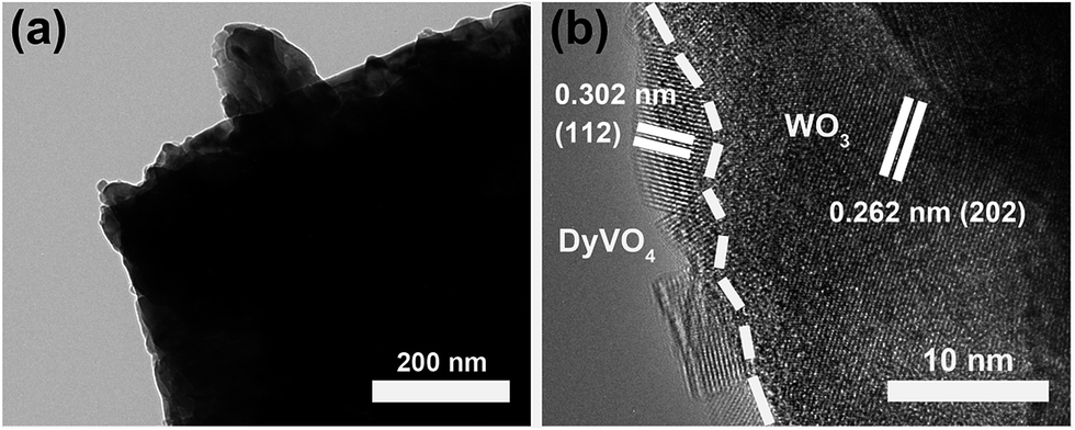 | ||
| Fig. 3 TEM image of DyVO4/WO3 film (a), HRTEM image of DyVO4/WO3 film (b). | ||
The composition of DyVO4/WO3 heterojunction film was detected by X-ray photoelectron spectroscopy (XPS). The analysis of XPS data was performed using the XPS Peak Fitting Program version 4.1. Fig. 4a shows the overall XPS survey spectrum, which confirms the existence of all the elements of DyVO4 and WO3. It is observed that W 4f7/2 and W 4f5/2 peaks are located at 35.4 eV and 37.5 eV, respectively (Fig. 4b), which is consistent with the W6+.24 The O 1s main peak in Fig. 4c was dissociated into two peaks: W–O (530.3 eV) and surface hydroxide –OH (531.6 eV).25 In addition, the peaks at 152.3 eV and 153.8 eV correspond to Dy 4d (Fig. 4e), and the V 2p peak was observed at 517.4 eV (Fig. 4d), which are in good agreement with the reported studies.26 Simultaneously, the potentials for top of the valence band (VB) for the samples were estimated (Fig. 4f). This result indicates that the introduction of DyVO4 nanoparticles results a 0.3 eV negative shift for the VB top edge of WO3.
 | ||
| Fig. 4 XPS spectra of the DyVO4/WO3 heterojunction film: (a) survey scan; (b) W 4f; (c) O 1s; (d) V 2p; (e) Dy 4d; (f) VB-XPS spectra. | ||
The UV-vis diffuse reflectance spectra of the WO3 and DyVO4/WO3 films are depicted in Fig. 5a. For pure WO3 film, the optical absorption edge is around 450 nm. The introduction of DyVO4 onto WO3 results in better absorption and a little red shift in the visible light range was observed. The band gap energy (Eg) of the samples was calculated by the Tauc formula:27
| (αhν)1/2 = A(hν − Eg) | (1) |
 | ||
| Fig. 5 UV-vis absorption spectra (a) and the band gap determination (b) of WO3 and DyVO4/WO3 heterojunction films. | ||
3.2 Photoelectrochemical measurements of as-prepared photoanodes
Linear sweep voltammetry (LSV) measurement was employed to investigate the PEC activities of the DyVO4/WO3 and WO3 films under visible irradiation (Fig. 6). The LSV was carried out with a potential range from 0 V to 1.5 V (vs. Ag/AgCl) with a scan rate of 20 mV s−1. The photocurrent densities of both films increased with applied potential under illumination. At +1.2 V (vs. Ag/AgCl), the photocurrent density of DyVO4/WO3 film was 0.78 mA cm−2, while the bare WO3 film exhibited a photocurrent of 0.49 mA cm−2. The DyVO4/WO3 heterojunction film exhibited an almost 1.59 times higher photocurrent density than the pure WO3 film under illumination. The enhanced PEC performance is probably due to the efficient photo-generated carriers' separation at the DyVO4/WO3 interface. | ||
| Fig. 6 Photocurrent densities (a) and IPCE (b) values of WO3 and DyVO4/WO3 films. | ||
To study the relationship between the PEC activity and the different wavelength of incident light, the incident-photon-to-current-efficiencies (IPCE) measurements were performed for WO3 and DyVO4/WO3 films at a bias voltage of 1.2 V (vs. Ag/AgCl) in 0.2 M Na2SO4 solution (Fig. 6b). IPCE can be expressed as IPCE = (1240I)/(λJlight),31 where I (mA cm−2), λ (nm) and Jlight (mW cm−2) are the photocurrent density, the wavelength and power density of incident light, separately. Both two films presented strong photo responses at 300–460 nm. However, the DyVO4/WO3 heterojunction film exhibited larger IPCE values than that of the WO3 film over the whole photo response region. The highest IPCE value of 54.11% was observed for DyVO4/WO3 film at 350 nm, which is almost 2 times higher than that of WO3 film (∼27.38%). Combining the UV-vis absorption spectra with the IPCE data, it demonstrates that the low content of deposited DyVO4 nanoparticles are not acted as a light photosensitizer.
Considering the importance of the stability of a photoelectrode for its practical application, the photocurrent–time plots of both films were obtained at +1.2 V vs. Ag/AgCl under discontinuous illumination. The results are shown in Fig. 7. After 5000 s, the pristine WO3 film shows about 47% decrease in photocurrent from 0.49 to 0.26 mA cm−2, while the DyVO4/WO3 film shows just about 17% decrease from 0.78 to 0.65 mA cm−2. This indicates that the introduction of DyVO4 improves the stability of WO3 film.
 | ||
| Fig. 7 Photocurrent–time plots of the photoelectrodes. | ||
To elucidate the strong correlation between formation of heterojunction and the enhanced photocurrent and IPCE values, Mott–Schottky analysis was conducted under the visible light irradiation with a frequency of 1 kHz in a 0.2 M Na2SO4 aqueous electrolyte. As presented in Fig. 8, both two films exhibited an n-type characteristic with the positive slop, which reflected that electrons served as the major carriers in DyVO4/WO3 heterojunction film. The electron density can be calculated based on the Mott–Schottky equation:32
| Nd = (2/εε0q)[d(1/C2)/dV]−1 | (2) |
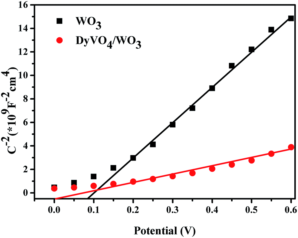 | ||
| Fig. 8 Mott–Schottky plots of WO3 and DyVO4/WO3 films. | ||
The flat band potential (Vfb) at semiconductor/electrolyte interface can also be estimated by the Mott–Schottky equation:36
| 1/C2 = (2/εε0qNd)[(V − Vfb) − kT/q] | (3) |
To investigate the electron transport properties in the electrode, the capacitance and resistance of the electrode materials which indicated the separation efficiency between the photo-generated electrons and holes,38 electrochemical impedance spectroscopy (EIS) of the as-prepared films were measured under the visible light illumination with a 0.8 V bias. Fig. 9a shows the typical Nyquist curve of the DyVO4/WO3 heterojunction film and pure WO3 film at an AC frequency varying from 10 kHz to 100 mHz. One semicircle is observed for each sample, suggesting that the faradaic charge transfer is the limiting step for the oxidation process in the electrode surface.32 The apparent difference in the impedance spectra was observed that the EIS Nyquist curve of DyVO4/WO3 film has a smaller circular radius than that of the pure WO3 film. The equivalent circuit consists of solution resistance (R1), charge transfer resistance (R2) in parallel to the constant phase element (CPE1).39 The resistance R1, R2 were calculated to be 25.3 Ω, 904.7 Ω for the WO3 film, and 35.4 Ω, 488.9 Ω for the DyVO4/WO3 film, respectively. The R1 values of both films are comparable while the R2 values are very different. This suggests that DyVO4/WO3 film owns lower charge transfer resistance than WO3 film, corresponding to the better PEC performance. Similarly, Bode plots in Fig. 9b reflect the efficient electron lifetime in WO3 and DyVO4/WO3 films. The lifetime (τe) can be calculated by τe = 1/(2πfmax), where the fmax is the frequency at which the frequency peak appears in the Bode plot.40 Larger τe values indicate that electrons have longer lifetime and faster diffusion rate in the photoelectrodes.41 As seen in Fig. 8b, the fmax value for WO3 is 67.7 Hz, while for DyVO4/WO3 is 18.6 Hz. The corresponding τe is 2.4 ms and 8.6 ms. This suggests that DyVO4/WO3 possesses an almost 4-fold improved lifetime of electrons compared with pure WO3 film.
 | ||
| Fig. 9 EIS Nyquist plots (a) and Bode plots (b) of WO3 and DyVO4/WO3 films. | ||
Actually, it is well known that the PEC activity of photocatalyst mainly depends on whether the electron–hole pairs can be separated effectively. The schematic for the DyVO4/WO3 heterojunction film illustrates the photo-generated carriers transport process, which can explain the possible mechanism for the enhanced PEC properties as shown in Fig. 10. Under the visible light irradiation, both DyVO4 and WO3 would be excited and produce the photo-generated electrons and holes, simultaneously. The DyVO4 has a more negative conduction band (CB) edge potential (−0.32 eV vs. NHE) and a valence band (VB) edge potential (1.98 eV vs. NHE) compared with WO3 (CB: 0.74 eV vs. NHE, VB: 3.44 eV vs. NHE),18,42 indicating that the photo-generated electrons of DyVO4 can easily transport into WO3, then transfer to the back-contacted FTO substrate through a direct pathway provided by the plates. Similarly, the photo-generated holes of WO3 will move to DyVO4 and take part in the oxygen evolution reaction. Thus, the photo-generated electron–hole pairs will be separated at the interface of the heterojunction and reduce the probability of recombination, which promote the PEC water splitting.
 | ||
| Fig. 10 Depiction of the energy level diagram of the DyVO4/WO3 film and the charge separation process. | ||
4. Conclusion
In summary, the DyVO4/WO3 heterojunction electrode consisting of two-dimensional WO3 plates arrays and DyVO4 nanoparticles were fabricated through a simple dipping-annealing method. Compared with the pure WO3 film, the DyVO4/WO3 heterojunction film possessed a higher photocurrent and a better PEC performance under visible light irradiation. On the basis of EIS, Mott–Schottky and IPCE, the DyVO4/WO3 heterojunction film owned longer electron lifetime, larger carriers density and more negative flat band potential. Besides that, the enhanced PEC performance of the heterojunction film was mostly attributed to the high separation and collection efficiency of photo-generated electron–hole pairs at the interface. The study demonstrates that metal orthovanadates may be good heterojunction candidates to couple with WO3 to provide promising photoanodes for water splitting.Acknowledgements
This study was supported by the National High Technology Research and Development Program of China (2011AA050528), the National Nature Science Foundation of China (51304253).References
- M. Yagi, S. Maruyama, K. Sone, K. Nagai and T. Norimatsu, J. Solid State Chem., 2008, 181, 175–182 CrossRef CAS.
- Z. Jiao, J. Wang, L. Ke, X. W. Sun and H. V. Demir, ACS Appl. Mater. Interfaces, 2011, 3, 229–236 CAS.
- F. Amano, D. Li and B. Ohtani, Chem. Commun., 2010, 46, 2769–2771 RSC.
- M. Qamar, Q. Drmosh, M. I. Ahmed, M. Qamaruddin and Z. H. Yamani, Nanoscale Res. Lett., 2015, 10, 54–59 CrossRef PubMed.
- W. Li, F. Zhan, J. Li, C. Liu, Y. Yang, Y. Li and Q. Chen, Electrochim. Acta, 2015, 160, 57–63 CrossRef CAS.
- M. Qamar, Z. H. Yamani, M. A. Gondal and K. Alhooshani, Solid State Sci., 2011, 13, 1748–1754 CrossRef CAS.
- Y. Choi, S. Kim, M. Seong, H. Yoo and J. Choi, Appl. Surf. Sci., 2014, 324, 414–418 CrossRef.
- J. Zhu, W. Li, J. Li, Y. Li, H. Hu and Y. Yang, Electrochim. Acta, 2013, 112, 191–198 CrossRef CAS.
- L. J. Zhang, S. Li, B. K. Liu, D. J. Wang and T. F. Xie, ACS Catal., 2014, 4, 3724–3729 CrossRef CAS.
- S. Wei, Y. Ma, Y. Chen, L. Liu, Y. Liu and Z. Shao, J. Hazard. Mater., 2011, 194, 243–249 CrossRef CAS PubMed.
- P. Zhao, C. X. Kronawitter, X. Yang, J. Fu and B. E. Koel, Phys. Chem. Chem. Phys., 2014, 16, 1327–1332 RSC.
- Y. He, L. Zhao, Y. Wang, H. Lin, T. Li, X. Wu and Y. Wu, Chem. Eng. J., 2011, 169, 50–57 CrossRef CAS.
- J. Ye, Z. Zou, M. Oshikiri, A. Matsushita, M. Shimoda, M. Imai and T. Shishido, Chem. Phys. Lett., 2002, 356, 221–226 CrossRef CAS.
- H. Xu, H. Wang and H. Yan, J. Hazard. Mater., 2007, 144, 82–85 CrossRef CAS PubMed.
- Y. He, J. Cai, L. Zhang, X. Wang, H. Lin, B. Teng, L. Zhao, W. Weng, H. Wan and M. Fan, Ind. Eng. Chem. Res., 2014, 53, 5905–5915 CrossRef CAS.
- W. Congsen, C. Xiaodong and L. Xue-Hong, Adv. Mater. Res., 2014, 1081, 146–150 CrossRef.
- S. J. Duclos, A. Jayaraman, G. Espinosa, A. Cooper and R. Maines, J. Phys. Chem. Solids, 1989, 50, 769–775 CrossRef CAS.
- Y. He, J. Cai, T. Li, Y. Wu, Y. Yi, M. Luo and L. Zhao, Ind. Eng. Chem. Res., 2012, 51, 14729–14737 CrossRef CAS.
- J. Zhang, P. Zhang, T. Wang and J. Gong, Nano Energy, 2015, 11, 189–195 CrossRef CAS.
- F. Amano, D. Li and B. Ohtani, J. Electrochem. Soc., 2011, 158, K42–K46 CrossRef CAS.
- J. Yang, W. Z. Li, J. Li, D. B. Sun and Q. Y. Chen, J. Mater. Chem., 2012, 22, 17744–17752 RSC.
- C. Liu, J. Li, Y. Li, W. Li, Y. Yang and Q. Chen, RSC Adv., 2015, 5, 71692–71698 RSC.
- X. Ma, J. Gong, S. Wang, F. He, H. Guo, X. Yang and G. Xu, J. Mol. Catal. A: Chem., 2005, 237, 1–8 CrossRef CAS.
- S. Han, J. Li, X. Chen, Y. Huang, C. Liu, Y. Yang and W. Li, Int. J. Hydrogen Energy, 2012, 37, 16810–16816 CrossRef CAS.
- M. M. Mohamed, S. A. Ahmed and K. S. Khairou, Appl. Catal., B, 2014, 150, 63–73 CrossRef.
- F. Guo, W. Shi, X. Lin, X. Yan, Y. Guo and G. Che, Sep. Purif. Technol., 2015, 141, 246–255 CrossRef CAS.
- A. Subrahmanyam and A. Karuppasamy, Sol. Energy Mater. Sol. Cells, 2007, 91, 266–274 CrossRef CAS.
- C. Santato, M. Odziemkowski, M. Ulmann and J. Augustynski, J. Am. Chem. Soc., 2001, 123, 10639–10649 CrossRef CAS PubMed.
- W. Z. Li, J. Li, X. Wang, J. Ma and Q. Y. Chen, Int. J. Hydrogen Energy, 2010, 35, 13137–13145 CrossRef CAS.
- W. Z. Li, J. Li, X. Wang, J. Ma and Q. Y. Chen, Appl. Surf. Sci., 2010, 256, 7077–7082 CrossRef CAS.
- Y. Ling, G. Wang, D. A. Wheeler, J. Z. Zhang and Y. Li, Nano Lett., 2011, 11, 2119–2125 CrossRef CAS PubMed.
- G. Wang, Y. Ling, D. A. Wheeler, K. E. George, K. Horsley, C. Heske, J. Z. Zhang and Y. Li, Nano Lett., 2011, 11, 3503–3509 CrossRef CAS PubMed.
- E. Salje and K. Viswanathan, Acta Crystallogr., Sect. A: Cryst. Phys., Diffr., Theor. Gen. Crystallogr., 1975, 31, 356–359 CrossRef.
- R. Sivakumar, A. M. E. Raj, B. Subramanian, M. Jayachandran, D. Trivedi and C. Sanjeeviraja, Mater. Res. Bull., 2004, 39, 1479–1489 CrossRef CAS.
- L. Su, L. Zhang, J. Fang, M. Xu and Z. Lu, Sol. Energy Mater. Sol. Cells, 1999, 58, 133–140 CrossRef CAS.
- N. T. Hahn and C. B. Mullins, Chem. Mater., 2010, 22, 6474–6482 CrossRef CAS.
- J. Zhang, J. H. Bang, C. Tang and P. V. Kamat, ACS Nano, 2009, 4, 387–395 CrossRef PubMed.
- W. D. Zhang, L. C. Jiang and J. S. Ye, J. Phys. Chem. C, 2009, 113, 16247–16253 CAS.
- S. K. Pilli, T. G. Deutsch, T. E. Furtak, L. D. Brown, J. A. Turner and A. M. Herring, Phys. Chem. Chem. Phys., 2013, 15, 3273–3278 RSC.
- F. Wang, Y. Wang, X. Zhan, M. Safdar, J. Gong and J. He, CrystEngComm, 2014, 16, 1389–1394 RSC.
- C. Zha, L. Shen, X. Zhang, Y. Wang, B. A. Korgel, A. Gupta and N. Bao, ACS Appl. Mater. Interfaces, 2013, 6, 122–129 Search PubMed.
- H. Katsumata, Y. Tachi, T. Suzuki and S. Kaneco, RSC Adv., 2014, 4, 21405–21409 RSC.
Footnote |
| † Electronic supplementary information (ESI) available. See DOI: 10.1039/c5ra22272a |
| This journal is © The Royal Society of Chemistry 2016 |