
Nano-grained ZrB2 thin films as a high-performance diffusion barrier in Cu metallization
Y. Menga,
F. Ma*a,
Z. X. Song*a,
Y. H. Li*a and
K. W. Xuab
aState Key Laboratory for Mechanical Behavior of Materials, Xi'an Jiaotong University, Xi'an 710049, Shaanxi, China. E-mail: mafei@mail.xjtu.edu.cn; zhongxiaosong@mail.xjtu.edu.cn; liyhemail@gmail.com; Fax: +86 029 82663453; Tel: +86 029 82663453
bDepartment of Physics and Opt-electronic Engineering, Xi'an University of Arts and Science, Xi'an 710065, Shaanxi, China
First published on 18th December 2015
Abstract
Nano-grained ZrB2 thin films are prepared by radio-frequency (rf) magnetron sputtering and, the thermal stability and the diffusion barrier performance are evaluated at elevated temperatures. It is demonstrated that the as-deposited ZrB2 thin films can effectively block the intermixing of Cu and Si atoms up to 700 °C. But substantial atomic diffusion occurs at 725 °C resulting in high-resistance CuSix compounds. A Cu3Si phase is formed at 750 °C and it has an epitaxial relationship with Si substrates, like, Cu3Si (000![[1 with combining macron]](https://www.rsc.org/images/entities/char_0031_0304.gif) )//Si (11) and Cu3Si (100)//Si (
)//Si (11) and Cu3Si (100)//Si (![[2 with combining macron]](https://www.rsc.org/images/entities/char_0032_0304.gif) 1). Although the crystallization of nano-grained ZrB2 thin films is enhanced at 700 °C, the high thermal stability makes it possible to be exploited as a diffusion barrier in Cu interconnects.
1). Although the crystallization of nano-grained ZrB2 thin films is enhanced at 700 °C, the high thermal stability makes it possible to be exploited as a diffusion barrier in Cu interconnects.
Introduction
Nowadays, integrated circuits (ICs) are moving towards smaller-technology nodes and, copper (Cu) has been the key interconnect material due to its low resistivity and excellent electro-migration resistance. However, the inter-diffusion and reaction between Cu and Si substrates still restrict the reliability of devices and have become a crucial issue in the field of microelectronics. The most effective way to suppress the inter-diffusion is to add a diffusion barrier between Cu interconnects and Si substrates, moreover, the adhesion between them should be improved.1–4A large number of researches have been done to exploit appropriate diffusion barrier materials for Cu metallization. Refractory transition metals, such as, Ta, Ti, Zr, Ru, characteristic of low resistivity and high thermal stability, become the research focus.5–8 Generally, pure metal thin films possess polycrystalline structure in which Cu atoms can diffuse along the grain boundaries and react with Si substrates at lower temperature. For example, 20 nm thick Ru diffusion barrier became failure at 450 °C.9 The current barrier materials adopted in Cu interconnection is Ta/TaN bilayer with a total thickness of 100 nm in which Ta serves as a glue layer and TaN is indeed the barrier layer. With the rapid development of Cu metallization, ultra-thin barrier layers with low resistivity and high thermal stability are needed. It was demonstrated that the crystallization of thin films could be suppressed through alloying and the thermal stability could be improved in the systems, such as, Ta–Si–N, Zr–Ti–Ni, Ta–W–C, Fe–Co–B–Ti–Nb and (AlCrTaTiZr)N.10–14 However, this makes the manufacturing process more complicated. The nitrogen in metal nitrides will effuse at a higher temperature and lead to crystallization.15 Oxides can prevent the atomic diffusion up to a high temperature but they possess almost the highest resistivity among all the compounds.16,17 Furthermore, although the temperature in the current IC fabrication process is about 400 °C, IC devices are often applied in some special fields, such as, in aerospace, in which higher working temperature might be met. For example, NASA introduced a new integrated circuit in the aircrafts in which the IC devices might operate at a temperature up to 600 °C.18 Hence, it is mandatory to exploit new materials with low resistivity but excellent stability at high temperatures for the rapid development of Cu metallization in the future.
Borides exhibit excellent physical properties, such as, low resistivity, high melting point, superb chemical inertness and good mechanical property. Particularly, zirconium diboride (ZrB2) has a low resistivity of 4.6 μΩ cm and a high melting point of 3220 °C.19 Moreover, both Zr and B have a negligible solubility in Cu20 and ZrB2 could epitaxially grow on Si (111), 4H–SiC (0001), GaN (0001) and Si (001) due to small lattice mismatch.21–24 This is beneficial to the structural stability and suppression of atomic diffusion in ZrB2 at high temperature. It has been reported that ZrB2 exhibits outstanding diffusion barrier performance in Si and GaAs technology. The as-deposited ZrB2 thin films were commonly nano-grained in A1B2 type hexagonal lattice.25 Sung J. et al.26 fabricated 20 nm ZrB2 films by remote plasma chemical vapor deposition (RPCVD) at 300 °C and found that the diffusion barrier could be maintained at 750 °C for 30 min. However, the excess B incorporation and oxide impurities in ZrB2 films prepared by CVD will increase the resistivity. As compared to CVD, magnetron sputtering is more compatible with the current fabrication process of integrated circuits and has higher deposition rate, the lowest cost and excellent reliability, and thus is the favored approach for deposition of ZrB2 barriers layers. Takeyama et al.25 deposited 3–300 nm ZrB2 films on glass, SiO2 and Cu substrates by magnetron sputtering, and demonstrated the potential diffusion barrier performance. However, the mechanism for diffusion barrier is still controversial.
In this paper, nano-grained ZrB2 thin films were prepared by radio-frequency (rf) magnetron sputtering and, the thermal stability and diffusion barrier performance were studied at elevated temperatures. It is demonstrated that the nano-grained ZrB2 films can effectively block the atomic diffusion at temperatures up to 700 °C. The diffusion barrier mechanism as well as the crystalline relationship between newly formed Cu3Si phase at 750 °C and Si substrate is uncovered.
Experimental details
Prior to deposition, both the Si (100) wafers and the targets were ultrasonically treated in acetone and alcohol for 10 minutes, respectively, to remove organic contaminants. The sputtering chamber was evacuated to a base pressure of 7.0 × 10⁻⁴ Pa. 15 nm thick ZrB2 films were first deposited on the substrates by rf magnetron sputtering in argon atmosphere at room temperature. A ZrB2 compound target (Φ 75 mm × 5 mm, 99.999% purity) was used. The Ar flow rate was 30 sccm. The sputtering pressure was 0.3 Pa and the sputtering power of ZrB2 was 80 W. 500 nm thick Cu capping layers were then deposited on the ZrB2 layer by using Cu target (Φ 75 mm × 5 mm, 99.999% purity). The samples were then annealed in a N2/H2 (N2![[thin space (1/6-em)]](https://www.rsc.org/images/entities/char_2009.gif) :H2 = 9:1) mixture atmosphere at 600–750 °C for 30 min.
:H2 = 9:1) mixture atmosphere at 600–750 °C for 30 min.
Phase structure of the thin films was characterized by a grazing incident X-ray diffractionmeter with Cu Kα radiation (GIXRD, XRD-7000, Shimadzu) at an incident angle of 1° and, the tube current and voltage were 40 mA and 40 kV, respectively. The measurement angle was scanned in the range of 30–80° with a scanning step of 0.02° and a scanning speed of 5° min−1. X-ray photoelectron spectroscopy (XPS, Thermo Scientific K-Alpha) was measured by using Al Kα radiation, the applied voltage and current were 12 kV and 6 mA, respectively. The measurements were done on surface and after etching for 10 s by 2 keV Ar+ with the etching rate of 0.28 nm s−1. Scanning Electron Microscope (SEM, FEI, QUANTA: 600F) was used to analyze the surface morphology of the films. The adhesion strength of the thin films was evaluated by using the nanoscratch test (Hysitron, Ti950 TriboIndenter) with a sphero-concial diamond tip indenter (tip radius ∼ 6 μm). A loading rate of 1 mN s−1 and a scratching rate of 5 μm s−1 were used. Five scratch tests were performed on each sample. Before the sheet resistance measurement, the samples were cut into 1 cm × 1 cm pieces. Five measurements were conducted for each Cu/ZrB2 thin film by RTS-9 four-point probe (FPP), and the average value was taken. High-Resolution Transmission Electron Microscopy (HRTEM, JEM-2100F) was employed to characterize the cross-section morphology as well as the evolution of the microstructures.
Results and discussion
Fig. 1(a) shows the XPS spectra of Zr and B in the as-deposited ZrB2 thin films. The dotted line denotes the bonding states on the surface, while the solid line represents the bonding states after ion etching. The peaks at the binding energies of 181.98 eV and 184.48 eV can be ascribed to ZrO2 and, the peaks at 177.78 eV and 180.18 eV is due to ZrB2.27,28 Apparently, ZrB2 on the surface are partially oxidized, but ZrO2 disappears after ion etching, indicating that the thin films are mainly composed of ZrB2. Taking into account the sensitivity factor of elements, the atomic ratio of Zr and B is calculated to be 1:2.03, close to that of the target. Fig. 1(b) displays the XRD pattern of the as-deposited ZrB2 thin films. The single diffraction peak at 2θ = 24.9° is ascribed to ZrB2 (0001) plane, and the wide full width at half maximum (FWHM) is consistent with the nano-grained configuration observed in TEM image. According to the FPP measurements, the ZrB2 thin films have a resistivity of 234.8 μΩ cm, slightly higher than the bulk value owing to a small amount of doped oxygen and the surface scattering.22 Even so, the value is still lower than the reported values of ternary alloys like Ta–Si–C (340 μΩ cm),12 Ta–Si–N (>600 μΩ cm)10 and multi-element alloys (AlCrTaTiZr)N (580 μΩ cm).14
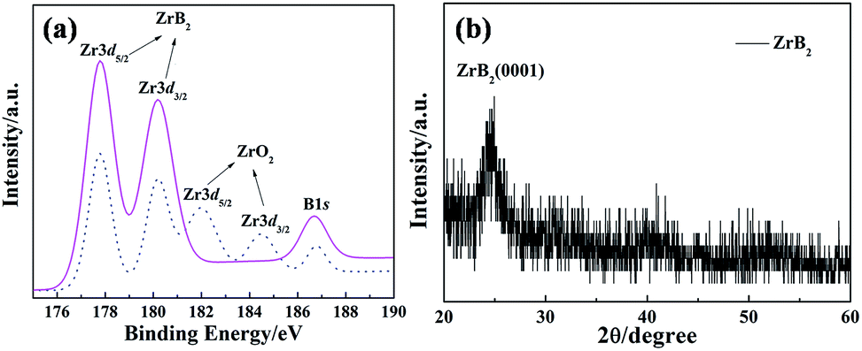 | ||
| Fig. 1 (a) XPS spectra of as-deposited ZrB2 films before and after Ar ion etching; (b) XRD pattern of ZrB2 thin films without Cu capping layer. | ||
Fig. 2 presents the XRD patterns of Cu/ZrB2 thin films as-deposited and thermally annealed at different temperatures. As for the as-deposited thin films, three XRD peaks are evidenced at 2θ = 43.4°, 50.6° and 74.3°, corresponding to the (111), (200) and (220) lattice planes of face-centered cubic (fcc) Cu, but no peaks of ZrB2 can be identified in the patterns. Actually, the thickness of ZrB2 thin films is 15 nm, which is much thinner than that of Cu thin films (500 nm). So the signal of nano-grained ZrB2 film and the Si substrates cannot be detected by GIXRD. Cu (111) is the preferred orientation, implying the excellent electro-migration resistance.29 The peak intensity increases with the annealing temperature, but the FWHM decreases as a result of enhanced crystallization of Cu films. When the annealing temperature is elevated up to 750 °C, whereas, the peak of high-resistance Cu3Si phase appears in the XRD spectra, indicating the inter-diffusion and reaction between Cu and Si atoms across ZrB2 diffusion barrier. The interstitial Si atoms are involved into Cu lattice, which will increase the lattice parameters and thus induce the shift of Cu (200) and Cu (220) peaks toward the lower angle. Besides Cu and Cu3Si, two other peaks at 2θ = 40.64° and 46.28° are also observed and could be assigned to Cu2O and Cu6.69Si, respectively. The formation of Cu2O is mainly due to partial oxidation of Cu films and Cu6.69Si is a non-equilibrium phase caused by reaction between Cu and Si. ZrB2 barrier layer is mixed into the fragmentary Cu thin films at such a high temperature. So no ZrB2 barrier layer can be detected by XRD even from the discontinuous Cu thin films.
 | ||
| Fig. 2 XRD patterns of the Cu/ZrB2 thin films samples as-deposited and after thermal annealed at different temperatures. | ||
Fig. 3 shows the SEM images of surface morphologies of the Cu films deposited on ZrB2 films. Apparently, the as-prepared thin films are smooth and contiguous, but the surface becomes rough owing to the grain growth upon thermal annealing, in particular, at higher temperature. When the annealing temperature is elevated up to 700 °C, grain aggregation occurs and some voids appear on the films which can be ascribed to the effect of surface tension of Cu films at high temperature. Simultaneously, the peak intensity of Cu (111) and (200) in XRD patterns decreases [Fig. 2]. Some CuSix grains are formed on the surface at 725 °C as a result of inter-diffusion and reaction between Cu and Si atoms, indicating that the failure of ZrB2 is indeed at 725 °C rather than at 750 °C. This is confirmed by the TEM images and the resistance measurement, as addressed in the following.
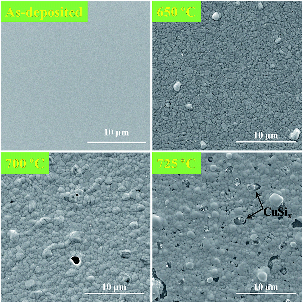 | ||
| Fig. 3 SEM images of the surface morphologies of the Cu/ZrB2 thin films. | ||
Nanoscratch tests are conducted to evaluate the adhesion strength of the thin films, the results are displayed in Fig. 4. Fig. 4(a) and (b) show the SEM images of the scratch profiles of the samples as-deposited and annealed at 400 °C, from which the delamination position can be determined. The scratch distance from the starting point to the delamination point is 64 μm and 95 μm for the as-deposited sample and that annealed at 400 °C. Accordingly, the critical load for the delamination of thin films can be obtained, and it is 13 mN and 19 mN for the as-deposited and the annealed ZrB2 thin films, respectively. The improved adhesion might be due to increased metallurgical bonding and stress release in the interface upon thermal annealing. The adhesion strength of ZrB2 thin films in our work is close to the value (15.55 mN) of Cu/Ta/DB/Si stacked layer reported by Liao C. et al.30 The adhesion strength is large enough for ZrB2 thin films applied as the barrier layer in Cu metallization.
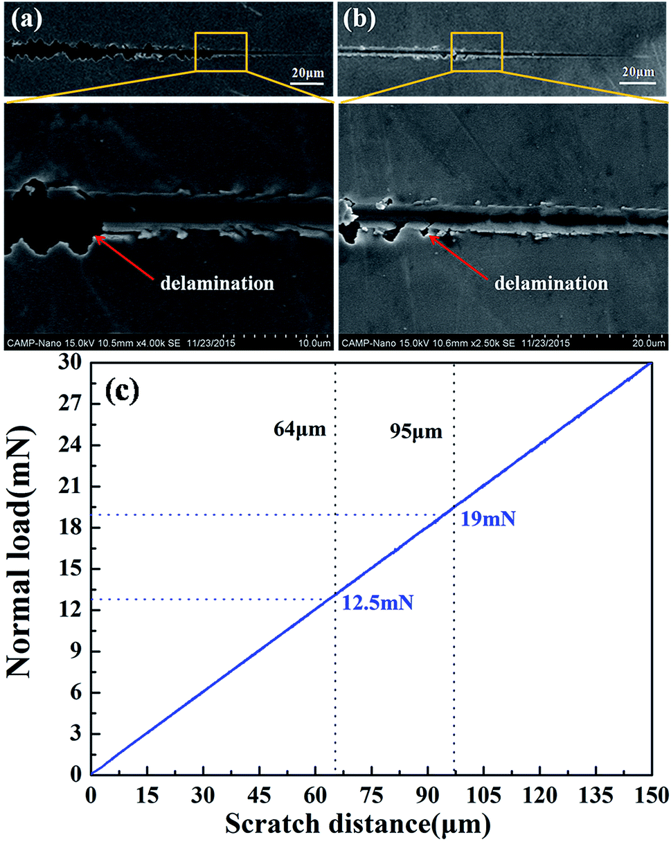 | ||
| Fig. 4 (a) and (b) SEM image of the nano-scratch profiles of the thin films as-deposited and annealed at 400 °C; (c) the scratch distance verse normal critical load. | ||
Four-point probe is adopted to measure the sheet resistance, and the average value of five measurements is taken for each Cu/ZrB2 thin film. Fig. 5 shows the measured sheet resistance with error bars as a function of the annealing temperature. The error fluctuation of the measured values is small, suggesting the high-accuracy measurement. The sheet resistance of the annealed films remains at a lower value than the as-grown samples up to 700 °C, which is mainly ascribed to the growth of Cu grains and the reduction of the defects in Cu films. Nevertheless, the sheet resistance increases substantially at 725 °C, indicating the formation of high-resistance CuSix and discontinuous Cu thin films because of the failure of the ZrB2 barrier layer. A sharp increase occurs when the annealing temperature is further elevated up to 750 °C, indicating the serious damage of the interconnection system.
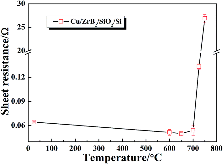 | ||
| Fig. 5 Sheet resistance as a function of the elevated annealing temperature. | ||
The cross-sectional TEM images of Cu/ZrB2/Si thin films are displayed in Fig. 6. As shown in Fig. 6(a) and (b), the as-prepared ZrB2 thin films exhibit a homogeneous morphology and adhere well with the Cu capping layer as well as Si substrates and, the nano-grained configuration of ZrB2 thin films is evident. Fig. 6(c) and (d) presents the TEM images of the Cu/ZrB2/Si stacked samples annealed at 700 °C. Sharp interface is still clearly visible in the as-deposited samples and no reaction can be observed between ZrB2 and the neighboring layers. In spite of enhanced crystallization, the nano-crystalline barrier layer still demonstrates excellent stability at high temperature. Fig. 6(e) and (f) show the FFT (Fast Fourier Transformation) patterns of Si layer and Cu layer from the local regions in Fig. 6(d), in which no diffraction spots of CuSix could be identified. It confirms that the inter-diffusion between Cu and Si is effectively suppressed even when the thin films are annealed at 700 °C. As reported previously, amorphous ZrN and W2N thin films with the same thickness of 15 nm could only prevent the inter-diffusion between Cu and Si up to 600 °C, and they have a high resistivity of 400 μΩ cm and 910 μΩ cm,31,32 respectively. RuAlO thin films with nano-crystalline structure exhibited a lower resistivity of 210 μΩ cm and failed at 650 °C.33 However, the ternary nature makes it difficult to maintain the process stability and the stoichiometric ratio of the films. ZrB2 thin films in our work have low resistivity of 234 μΩ cm and the highest failure temperature of 725 °C. Moreover, it is easy to control the chemical components of the binary ZrB2 thin films. Hence, the nano-grained ZrB2 films exhibit the high performance. Since the diameter of the electron beam spot in TEM is about 140 nm, much larger than the thickness of ZrB2 barrier (15 nm). The Selected Area Electron Diffraction (SAED) and Energy Dispersive X-ray Spectrum (EDX) of ZrB2 layer are covered by Cu and Si signal and cannot be identified. Table 1 presents the EDX results of the thin films annealed at 700 °C and 725 °C, the regions measured are marked in Fig. 6(a) and 7(a). As the annealing temperature is elevated up to 725 °C, the nano-grains in ZrB2 thin films grow into large polycrystalline grains and the boundaries could provide the effective diffusion paths, and CuSix grains appear at the interface [Fig. 7(d)]. According to the EDX data, the CuSix phase is Cu rich. The result is in agreement with the SEM image [Fig. 3] and the increased sheet resistance [Fig. 5]. The HRTEM image [Fig. 7(b)] and the SAED pattern of Si layer [Fig. 7(c)] indicate the single-crystalline feature. As shown in Fig. 7(e) and (f), no CuSix phase appears in Cu films far away from the interface. When the annealing temperature is further elevated up to 750 °C, the barrier is seriously damaged and Cu thin films become discontinuous, so it is nearly impossible to obtain the separate EDX, HRTEM information from each layer. Fig. 8(a) and (b) highlighted the HRTEM images of the as-deposited ZrB2 thin film and that annealed at 725 °C. Apparently, the nano-grains in ZrB2 thin films grow into large polycrystalline ones at an annealing temperature of 725 °C. Accordingly, a schematic model is proposed to better understand the atomic diffusion mechanism. As schematically shown in Fig. 8(c) and (d), Cu atoms commonly diffuse along the grain boundaries of nano-grains and polycrystalline ones because of the incompact atom arrangement in the local regions. The zigzag grain boundaries in the nano-grained barrier layers will prolong the diffusion path and thus suppress the atom diffusion. However, the nano-grains will grow into polycrystalline ones with more straight diffusion path when the thin films are annealed at high temperatures. In such a case, it becomes easier for inter-diffusion between Cu and Si.
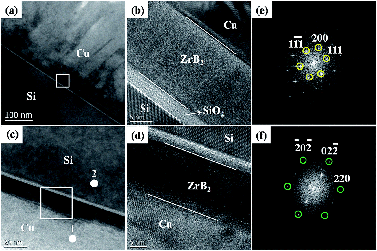 | ||
| Fig. 6 Cross-sectional TEM images of Cu/ZrB2/Si samples: (a) and (b) the as-deposited ones; (c) and (d) those annealed at 700 °C; (e) and (f) the corresponding FFT patterns of Si and Cu layers. | ||
| 1 | 2 | 3 | 4 | 5 | |
|---|---|---|---|---|---|
| Cu | 95.79 | 2.69 | 90.54 | 94.07 | 86.88 |
| Zr | 2.37 | — | — | — | — |
| Si | 1.84 | 97.31 | 9.46 | 5.93 | 13.12 |
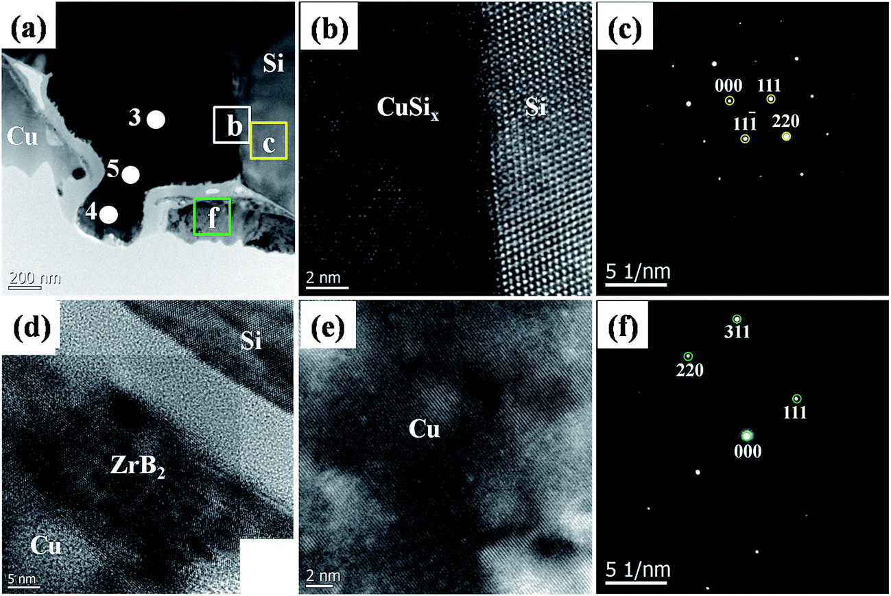 | ||
| Fig. 7 Cross-sectional TEM images of Cu/ZrB2/Si annealed at 725 °C: (a) the low magnification image; (b) HRTEM image of the interface of CuSix and Si; (c) and (f) SAED pattern of Si and Cu layer; (d) and (e) HRTEM image of Cu/ZrB2/Si and Cu. | ||
 | ||
| Fig. 8 HRTEM images of ZrB2 films as-deposited (a) and annealed at 725 °C (b); schematic models of atomic diffusion in thin films of nano-grains (c) and large polycrystalline grains (d). | ||
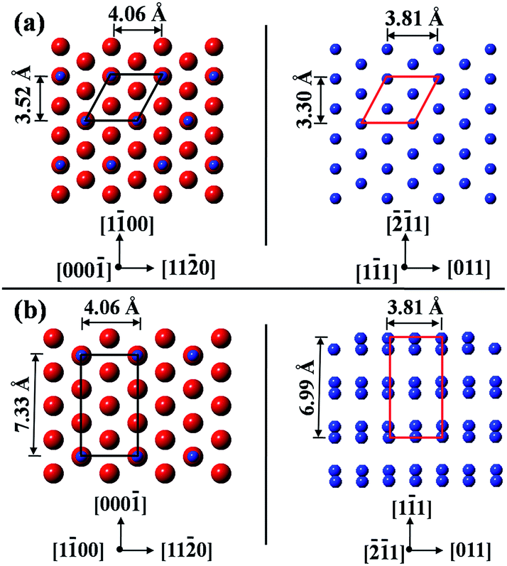
As displayed in Fig. 9(a) and measured by point spectra, Cu3Si compound is formed at 750 °C in the Si matrix and the high-resolution TEM image of the interface is presented in Fig. 9(b). Fig. 9(d) and (f) show the SAED patterns of Cu3Si and Si along a zone axial of [110] and [011], respectively. Fig. 9(e) presents the combined one in which the SAED patterns of Cu3Si and Si coincide at some spots, demonstrating the epitaxial relationship between Cu3Si and Si. The detailed epitaxial relationship is Cu3Si (000)//Si (11) and Cu3Si (100)//Si (1). The satellite spots in Fig. 9(d) can be ascribed to the long-period anti-phase domains.34 Fig. 9(c) shows the edge dislocation distribution at the interface and the dislocation density is calculated to be 5.33 × 1012 cm−2. As reported previously,35 Cu3Si has three phases, η, η′ and η′′ but similar lattice structure. η′′ phase is an equilibrium phase at room temperature and will transform into η′ phase at a 531 °C and then to η phase at 600 °C. The η′′ Cu3Si phase and the diamond-cubic Si are considered to study the epitaxial relationship. Fig. 10 shows the modeled atomic arrangement. Although hexagonal Cu3Si has the lattice structure different from diamond-cubic Si, some epitaxial relationship still exists between them. As for Cu3Si (000)//Si (11) planes, Si atoms in both Cu3Si and Si are arranged in a rhombohedral lattice with two in-plane epitaxial directions along Cu3Si [100]//Si [1] and Cu3Si [110]//Si [011]. But for the Cu3Si (100)//Si (1) plane, Si atoms are arranged in rectangle structure with two in-plane epitaxial directions along Cu3Si [000]//Si [11] and Cu3Si [110]//Si [011]. Table 2 lists the mismatch degree in the epitaxial planes. In the Cu3Si (000)//Si (11) planes, the mismatch along Cu3Si [110]//Si [011] direction is 6.16%, but is 6.25% along Cu3Si [100]//Si [1] direction. In the Cu3Si (000)//Si (1) planes, the mismatches along Cu3Si [110]//Si [011] and Cu3Si [000]//Si [11] are 6.16% and 4.64%, respectively. Apparently, the mismatch in all epitaxial planes is lower than 10%, corresponding to the low dislocation density mentioned above.
 | ||
| Fig. 9 Cross-sectional TEM images of Cu/ZrB2/Si annealed at 750 °C: (a) the low magnification image with an EDX profile of Cu3Si in the inset; (b) high resolution TEM image from the local region in (a); (c) the inverse FFT image from the (11) spot in (f); (d)–(f) the SAED patterns of Cu3Si, the interface and Si respectively. | ||
 | ||
| Fig. 10 Modeled atomic arrangements of Cu3Si and Si in the epitaxial direction: (a) Cu3Si (000)//Si (11); (b) Cu3Si (100)//Si (1). | ||
| Epitaxial plane | Epitaxial orientation | Mismatch |
|---|---|---|
| Cu3Si (000)//Si (11) |
Cu3Si [100]//Si [1] |
6.25% |
| Cu3Si [110]//Si [011] |
6.16% | |
| Cu3Si (100)//Si (1) |
Cu3Si [110]//Si [011] |
6.16% |
| Cu3Si [000]//Si [11] |
4.64% |
Conclusion
In this study, nano-grained ZrB2 thin films and Cu capping layers were deposited on Si (100) substrates by magnetron sputtering. The thermal stability and diffusion barrier performance for the barrier layer against inter-diffusion of Cu and Si atoms were evaluated via thermal annealing at different temperatures. XRD patterns, sheet resistance measurement and TEM images indicated that ZrB2 thin films exhibited excellent thermal stability and the sharp and uniform interfaces between the barrier layer and the adjacent layers were kept up to 700 °C. When the annealing temperature was elevated up to 725 °C, the ZrB2 barrier layer failed and CuSix compound was formed. Nano-scratch test demonstrated that the adhesion strength is large enough for ZrB2 thin films applied as the barrier layer in Cu metallization. Moreover, Cu3Si phase is formed at 750 °C and it has an epitaxial relation with Si substrates, as Cu3Si (000)//Si (11) and Cu3Si (100)//Si (1). All in all, the nano-grained ZrB2 thin films can effectively block the diffusion up to 700 °C and can be adopted as a diffusion barrier in Cu interconnect technology.
Acknowledgements
This work was supported by the National Natural Science Foundation of China (Grant No. 51471130, 51271139 and 51271140), the Natural Science Foundation of Shaanxi Province (2013JM6002), Fundamental Research Funds for the Central Universities.Notes and references
- J. H. Bong, S. J. Yoon, A. Yoon, W. S. Hwang and B. J. Cho, Appl. Phys. Lett., 2015, 106, 063112 CrossRef.
- Y. Chung, S. Lee, C. Mahata, J. Seo, S.-M. Lim, M. Jeong, H. Jung, Y.-C. Joo, Y.-B. Park, H. Kim and T. Lee, RSC Adv., 2014, 4, 60123–60130 RSC.
- Y. Meng, Z. X. Song, D. Qian, W. J. Dai, J. F. Wang, F. Ma, Y. H. Li and K. W. Xu, J. Alloys Compd., 2014, 588, 461–464 CrossRef CAS.
- H. Y. Wong, N. F. Mohd Shukor and N. Amin, Microelectron. J., 2007, 38, 777–782 CrossRef CAS.
- T. N. Arunagiri, Y. Zhang, O. Chyan, M. EI-Bouanani, M. J. Kim and K. H. Chen, Appl. Phys. Lett., 2005, 86, 083104 CrossRef.
- B. Liu, Z. X. Song, Y. H. Li and K. W. Xu, Appl. Phys. Lett., 2008, 93, 174108 CrossRef.
- X. P. Qu, J. J. Tan, M. Zhou, T. Chen, Q. Xie, G. P. Ru and B. Z. Li, Appl. Phys. Lett., 2006, 88, 151912 CrossRef.
- L. W. Lin, B. Liu, D. Ren, C. Y. Zhan, G. H. Jiao and K. W. Xu, Surf. Coat. Technol., 2013, 228, S237–S240 CrossRef CAS.
- R. Chan, T. N. Arunagiri, Y. Zhang, O. Chyan, R. M. Wallace, M. J. Kim and T. Q. Hurd, Electrochem. Solid-State Lett., 2004, 7, G154 CrossRef CAS.
- J. S. Reid, E. Kolawa, R. P. Ruiz and M.-A. Nicolet, Thin Solid Films, 1993, 236, 319–324 CrossRef CAS.
- C. W. Wang, P. Yiu, J. P. Chu, C. H. Shek and C. H. Hsueh, J. Mater. Sci., 2015, 50, 2085–2092 CrossRef CAS.
- J. S. Fang, W. J. Su, M. S. Huang, C. F. Chiu and T. S. Chin, J. Electron. Mater., 2013, 43, 212–218 CrossRef.
- J. S. Fang, L. C. Yang and Y. C. Lee, J. Alloys Compd., 2014, 586, S348–S352 CrossRef CAS.
- S. Y. Chang, M. K. Chen and D. S. Chen, J. Electrochem. Soc., 2009, 156, G37–G42 CrossRef CAS.
- M. Damayanti, T. Sritharan, S. G. Mhaisalkar and Z. H. Gan, Appl. Phys. Lett., 2006, 88, 044101 CrossRef.
- P. Majumder, R. Katamreddy and C. Takoudis, Electrochem. Solid-State Lett., 2007, 10, H291–H295 CrossRef CAS.
- C. M. Liu, W. L. Liu, W. J. Chen, S. H. Hsieh, T. K. Tsai and L. C. Yang, J. Electrochem. Soc., 2005, 152, G234–G239 CrossRef CAS.
- P. G. Neudeck, M. J. Krasowski and N. F. Prokop, ECS Trans., 2011, 41, 163–176 CAS.
- M. Samuelsson, J. Jensen, U. Helmersson, L. Hultman and H. Högberg, Thin Solid Films, 2012, 526, 163–167 CrossRef CAS.
- C. E. Ramberg, E. Blanquet, M. Pons, C. Bernard and R. Madar, Microelectron. Eng., 2000, 50, 357–368 CrossRef CAS.
- R. Roucka, J. Tolle, A. V. G. Chizmeshya, I. S. T. Tsong and J. Kouvetakis, J. Cryst. Growth, 2005, 277, 364–371 CrossRef CAS.
- L. Tengdelius, M. Samuelsson, J. Jensen, J. Lu, L. Hultman, U. Forsberg, E. Janzén and H. Högberg, Thin Solid Films, 2014, 550, 285–290 CrossRef CAS.
- A. Fleurence, W. Zhang, C. Hubault and Y. Yamada-Takamura, Appl. Surf. Sci., 2013, 284, 432–437 CrossRef CAS.
- J. Tolle, R. Roucka, I. S. T. Tsong, C. Ritter, P. A. Crozier, A. V. G. Chizmeshya and J. Kouvetakis, Appl. Phys. Lett., 2003, 82, 2398 CrossRef CAS.
- M. B. Takeyama, A. Noya, Y. Nakadai, S. Kambara, M. Hatanaka, Y. Hayasaka, E. Aoyagi, H. Machida and K. Masu, Appl. Surf. Sci., 2009, 256, 1222–1226 CrossRef CAS.
- J. Sung, D. M. Goedde, G. S. Girolami and J. R. Abelson, J. Appl. Phys., 2002, 91, 3904–3911 CrossRef CAS.
- M. Brochu, B. D. Gauntt, L. Boyer and R. E. Loehman, J. Eur. Ceram. Soc., 2009, 29, 1493–1499 CrossRef CAS.
- T. G. Wang, Y. Liu, T. Zhang, D. I. Kim and K. H. Kim, J. Mater. Sci. Technol., 2012, 28, 981–991 CAS.
- C. Ryu, K. W. Kwon, A. L. S. Loke, H. Lee, T. Nogami, V. M. Dubin, R. A. Kavari, G. W. Ray and S. S. Wong, IEEE Trans. Electron Devices, 1999, 46, 1113–1120 CrossRef CAS.
- C. L. Liao, D. Guo, S. Z. Wen, X. C. Lu, G. S. Pan and J. B. Luo, Tribol. Lett., 2013, 53, 401–410 CrossRef.
- S. Cho, K. Lee, P. Song, H. Jeon and Y. Kim, Jpn. J. Appl. Phys., 2007, 46, 4085–4088 CrossRef CAS.
- B. H. Lee and K. Yong, J. Vac. Sci. Technol., B, 2004, 22, 2375 CAS.
- T. Cheon, S.-H. Choi, S.-H. Kim and D.-H. Kang, Electrochem. Solid-State Lett., 2011, 14, D57 CrossRef CAS.
- F.-W. Yuan, C.-Y. Wang, G.-A. Li, S.-H. Chang, L.-W. Chu, L.-J. Chen and H.-Y. Tuan, Nanoscale, 2013, 5, 9875–9881 RSC.
- J. K. Solberg, Acta Crystallogr., Sect. A, 1978, 34, 684–698 CrossRef.
| This journal is © The Royal Society of Chemistry 2016 |