DOI:
10.1039/C5RA20461E
(Paper)
RSC Adv., 2016,
6, 20074-20080
SiO2–Ti0.98In0.01Nb0.01O2 composite ceramics with low dielectric loss, high dielectric permittivity and an enhanced breakdown electric field†
Received
3rd October 2015
, Accepted 5th February 2016
First published on 9th February 2016
Abstract
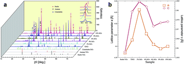
SiO2–Ti0.98In0.01Nb0.01O2 (SiO2–TINO) composite ceramics were synthesized by solid-state sintering methods. The dielectric loss can be lowered and the breakdown electric field can be greatly enhanced by doping 2 mol% SiO2 into TINO ceramics, while preserving the relatively high dielectric permittivity (∼30
000). The microstructure and electrical response of SiO2–TINO composite ceramics were studied to investigate the reasons for these good dielectric properties. The lower dielectric loss and enhanced breakdown electric field were attributed to the embedding of SiO2 in the TINO grain boundaries, which induced a drop in the potential and a blocking effect around the grain boundaries for the 2 mol% SiO2–TINO composite ceramic. The results provide a way to lower the dielectric loss and enhance the breakdown voltage by tuning the grain boundary.
Introduction
Materials with colossal permittivity (CP, i.e., a relative dielectric permittivity larger than 1000) are of focal interest because of their potential use in smaller and faster electronics. Recently, remarkable dielectric behavior has been reported in (Nb + In) co-doped TiO2 (TINO) ceramics,1 which possess colossal dielectric permittivity (>104) over a wide temperature range from 80 to 450 K and show potential to replace state-of-the-art CP materials, such as CaCu3Ti4O12 (ref. 2) and doped-BaTiO3.3
However, the dielectric loss was found to be susceptible to the sintering schedule (i.e., heating rate, cooling rate, sintering temperature, holding time, and sintering atmosphere), and the breakdown electric field was quite low for TINO ceramics. These disadvantages may inhibit further application of these ceramics.1b,g Thus, decreasing the dielectric loss and enhancing the breakdown electric field is important for TINO ceramics. Although the origin of the colossal dielectric permittivity is still an open question,1 the conductivity of the grain boundary was thought to play an important role in the high dielectric loss of TINO ceramics.1c,g From the methods employed in other CP ceramics (adding CaTiO3,4 La2O3,5 ZrO2,6 NiO,7 Al2O3,8 SiO2,9 and MnO10 to decrease dielectric loss), we chose SiO2 to dope into TINO ceramics to achieve a low dielectric loss and high breakdown electric field, because SiO2 possesses large band-gap energy and high resistance. The results demonstrated that the secondary SiO2 phase that aggregated around the grain boundaries could decrease the dielectric loss and enhance the breakdown electric field; meanwhile, a high dielectric permittivity of ∼30
000 was preserved.
Results and discussion
Fig. 1a shows the XRD powder patterns for SiO2–TINO composite ceramics, where the XRD peaks of rutile TiO2, anatase TiO2, and cristobalite SiO2 are also shown to confirm the phase structure of prepared ceramics. The lattice planes of the rutile phase are given according to the XRD card. The XRD patterns showed that a second phase of SiO2 and a minor anatase phase existed in all SiO2–TINO ceramics. The inset of Fig. 1a shows the shift of the (101) plane peak with increasing SiO2, indicating the change of the lattice parameters of TiO2. The lattice parameters (a, c) exhibited a maximum value when the TINO ceramics were doped with 2 mol% SiO2, dropping remarkably with the addition of SiO2; however, a slight increase appeared at a high doping level (>6 mol%), as shown in Fig. 1b. The change of the lattice parameter was thought to be induced by the SiO2 phase transition during the cooling stage and not by diffusion of Si(IV) cations, leading to an internal stress/strain of the grains. As the Ti (radius 0.605 Å (ref. 13)) occupy the center site to form [TiO6] octahedrons, Si(IV) (radius 0.4 Å (ref. 13)) occupy the center site to form [SiO4] tetrahedrons. According to solid solution law, |0.605 − 0.4/0.605| = 34% is much higher than the infinite solid solution's upper limit (15%). Therefore, Si(IV) cannot replace the Ti(IV) in the [TiO6] octahedron.
 |
| Fig. 1 Phase structure of the TINO and SiO2–TINO composite ceramics. (a) The XRD powder patterns and (b) calculated lattice parameters. | |
To analyze the elemental distribution in the prepared ceramics, SEM mapping experiments were employed, as shown in Fig. 2. The overlap mapping image in Fig. 2b shows a green region corresponding to SiO2 grains, and a red region corresponding to TINO grains, which was verified by the subsequent EDS images (Fig. 2c–f). Fig. 2c and d clearly show the scattered SiO2 particles among the TINO grains. However, the In (Fig. 2e) and Nb (Fig. 2f) EDS mapping image was blurry and had weak signals owing to their low doping concentration. Meanwhile, it was observed from Fig. 2c that some of the SiO2 particles seem to be segregated around TiO2 grain boundaries, indicating weak or even negligible diffusion between SiO2 and TINO grains.
 |
| Fig. 2 Element distribution of the SiO2–TINO composite ceramic. (a) SEM images for 2 mol% SiO2–TINO ceramics. (b) The X-ray element (Si, Ti, In, Nb) overlap mapping EDX image. The following EDX images were the respective mapping image of Si (c), Ti (d), In (e) and Nb (f). | |
HAADF-STEM images were used to confirm that the SiO2 particles were embedded around the TiO2 grain boundaries, as shown in Fig. 3. Additionally, it is clear from the line scanning (lower inset of Fig. 3a) and map scanning (upper right inset of Fig. 3a) elemental distribution analysis that the Si(IV) did not diffuse into the TINO grains. This was also verified by the plane-view TEM image (Fig. 3b) of the same region shown in the upper left image in Fig. 3a, and the selected area electron diffraction (SAED) spots for the marked region around the grain boundary (left image in Fig. 3b), indicating the good crystalline structure of the TINO and SiO2 particles. Meanwhile, the SAED spots of regions I, II and III were recorded along the [
11], [
22] and [
11] zone axis, respectively. The lattice planes in each SAED pattern were also given according to the d-spacing of rutile TiO2 and cristobalite SiO2.
 |
| Fig. 3 SiO2 segregated around gain boundaries in the SiO2–TINO composite ceramic. (a) The left-upper was the HAADF STEM image. (b) Left image was the plane-view TEM image of the same region. Right images were the Selected Area Electron Diffraction (SAED) spots. | |
To observe the surface potentials around the grain boundary,14 scanning Kelvin probe force microscopy (KPFM) was used, as shown in Fig. 4. The top image in Fig. 4 clearly shows a smooth surface with a roughness of less than 20 nm and no notable variation in the surface, which was a prerequisite for the surface potential test. Under lift mode KPFM the probe was uplifted about 50 nm and a lateral bias of 50 V was applied between the tip of the probe and the surface of the sample, as shown in Fig. 4 middle-lower schematic diagram. Fig. 4 (bottom image) shows that the potential across the SiO2 band dropped in the plane view and three-dimensional (3D) image, confirming the existence of an electrostatic barrier around the grain boundary, which is thought to be responsible for the lower dielectric loss and high breakdown voltage in the SiO2–TINO composite ceramics.
 |
| Fig. 4 Surface potential microscopy of the SiO2–TINO composite ceramic. Left-upper was the surface topographic image with AFM. Right-upper and right-lower were the 3D view of surface topographic image and surface potential image, respectively. | |
Fig. 5 shows the XPS data and fitting lines of Ti 2p (a), Nb 3d (b), Si 2p (c), O 1s (d) and In 3d (e) for the surface of the 2 mol% SiO2–TINO ceramics. The Ti 2p spectra (Fig. 5a) consisted of well-defined Ti(IV) 2p1/2 and Ti(IV) 2p3/2 photoelectron signals, which were located near 464 and 458 eV, respectively. The spin–orbital splitting between the Ti(IV) 2p peaks was nearly constant at approximately 5.74 eV. The split singlet of O 1s revealed the existence oxygen vacancies.15 Fig. 5d shows the peak positions of the O 1s orbital at 529.9 and 531.1 eV, associated with the Ti–O bond and oxygen vacancy in the rutile TiO2 structure, respectively. According to the literature,16 the O 1s state always contains a low binding energy peak (LP) and a high binding energy peak (HP) centered at approximately 529.77 and 531.27 eV. The LP and HP were attributed to O(II) at the intrinsic sites and the O(II) in the oxygen deficient regions. The LP and HP were nearly the same strength, indicating that the oxygen existed in oxygen deficient states.
 |
| Fig. 5 Element valence state of 2 mol% SiO2–TINO ceramics. Experimental XPS data (open circles) of Ti 2p (a), Nb 3d (b), Si 2p (c), O 1s (d), In 3d (e). | |
The singlet of Si 2p indicated that only an Si(IV) valence state existed in the sample. No extremely weak low-binding-energy shoulder was apparent for the Nb 3d and In 3d spin–orbit doublet, indicating that they had a single valence state in the specimen. The doublet of Nb 3d and In 3d indicated the existence of Nb(IV) and In(III) in the samples,2a respectively. It is generally accepted that Nb(IV) is a donor dopant and In(III) is acceptor dopant in the rutile TiO2 structure.
Fig. 6a shows the dielectric permittivity and loss with respect to frequency for SiO2–TINO ceramics. It was demonstrated that the TINO ceramics possessed the highest dielectric permittivity and loss. Fig. 6b compares the dielectric permittivity and loss of various ceramics measured at 1 kHz. The dielectric permittivity decreased with increasing SiO2 up to 6 mol%, and increased slightly at high doping >6 mol%. The dielectric loss decreased drastically from 0.176 to 0.043 with the addition of 2 mol% SiO2, and then slightly increased to 0.06 with 6 mol% doping; it increased unusually highly when doped with more SiO2. It should be noted that among these ceramics TINO ceramics doped with 2 mol% SiO2 possessed the highest dielectric permittivity (33
600) and lowest dielectric loss (0.043).
 |
| Fig. 6 Dielectric behaviour of TINO and SiO2–TINO composite ceramics. (a) Dielectric permittivity and loss with respect to frequency. (b) The dielectric permittivity and loss measured at 1 kHz. | |
It is noteworthy that the lowest dielectric loss displayed by the 2 mol% SiO2–TINO ceramic (shown in Fig. 6b) was associated with the highest resistance (15 MΩ) of the grain boundary, as shown in Fig. 7. The impedance spectroscopy (IS) for various compositions was plotted with the real part Z′ as the abscissa and imaginary part −Z′′ as the ordinate. The Z′ and −Z′′ of the complex impedance were given as follows:
|
Z′ = Rg/[1 + (ωτg)2] + Rgb/[1 + (ωτgb)2]
| (1) |
|
−Z′′ = Rgωτg/[1 + (ωτg)2] + Rgbωτgb/[1 + (ωτgb)2],
| (2) |
where
Rg and
Cg are the resistance and capacitance of the grain (here, corresponding to the TINO main phase), respectively.
17 Rgb and
Cgb are the resistance and capacitance of grain boundary (including the contribution of the SiO
2 particle), respectively. The relaxation times
τg and
τgb can be calculated by
τg =
RgCg and
τgb =
RgbCgb, respectively.
ω is the angular frequency, which is equal to 2π
f.
17 Fig. S4a and b
† show the enlarged view of the high frequency region, clearly showing the separate grain boundary arc and grain arc in 4 mol% and 8 mol% SiO
2–TINO ceramics. However, the other compositions didn't show the separate grain boundary arc and grain arc, which was thought to be associated with the overlap of two arcs.
 |
| Fig. 7 Impedance spectroscopy of SiO2–TINO composite ceramics. The solid symbols were the experimental results. The solid lines corresponding to each solid symbol were the best fitting results according to eqn (1) and (2). | |
Fig. 8 shows the temperature dependence of the dielectric permittivity measured at various frequencies (0.1–1000 kHz) for 2 mol% SiO2–TINO ceramics. It is clear that the dielectric permittivity decreases with increasing test frequency; although the dielectric permittivity slightly increased with increasing temperature, it also exhibited temperature-independent properties in the range from −55 to 150 °C. It should be noted that the dielectric loss obtained at 1 kHz was below 0.05 over almost the whole temperature range. At high temperatures, both the real and imaginary parts of the permittivity increased at low frequencies, indicating a strong dispersion. This dielectric contribution appeared at 100 °C at 0.1 Hz in all the samples. Such a contribution has often been observed at high temperatures in perovskite ceramics. It was most probably caused by the relaxation of the mobile charge carriers and had no immediate relation to the present CP phenomena. Therefore, we did not consider this dispersion in the present work.
 |
| Fig. 8 Temperature dependence of SiO2–TINO composite ceramics. Dielectric permittivity and loss of 2 mol% SiO2–TINO ceramics in range from −55 to 150 °C (the temperature range of X8R). | |
Fig. 9a shows the current density–electric field characteristics for TINO and 2 mol% SiO2–TINO ceramics. The HAADF-STEM and KPFM experiments showed that the breakdown voltage of the 2 mol% SiO2–TINO composite ceramic was much higher than that of the TINO ceramic, which was attributed to the strong blocking effect around the grain boundaries in 2 mol% SiO2–TINO composite ceramic. Fig. 9b shows the mean and standard errors of the dielectric loss versus frequency between the TINO and 2 mol% SiO2–TINO composite ceramics (the data was from ten sets of ceramics prepared using the same procedures). Clearly, the 2 mol% SiO2–TINO composite ceramic had a much lower dielectric loss and fluctuation compared with the TINO ceramics, which was also thought to be associated with the strong blocking effect around the boundaries after doping with SiO2. As for the TINO ceramic, it was susceptible to the sintering schedule, especially the cooling rate and sintering temperature. In contrast, the dielectric and electrical performance of SiO2–TINO ceramic was not influenced by the sintering schedule.
 |
| Fig. 9 Current density–electric field characteristics and the mean and standard error comparison of TINO and SiO2–TINO composite ceramics. (a) Current density–electric field characteristics. (b) The mean and standard errors of dielectric loss versus frequency. | |
Experimental
Materials and methods
The 1 mol% (Nb + In) co-doped TiO2 (TINO) ceramics were first sintered at 1400 °C for 10 h by standard conventional solid-state method, where the rutile TiO2 (99.99%), Nb2O5 (99.99%) and In2O3 (99.99%) powders were used as raw materials. The prepared TINO ceramic was milled to a powder in a ball-milling jar for 4 h in distilled water with Y-stabilized ZrO2 media. After drying, the SiO2 (99.99%) powders were added in stoichiometric proportions (0, 2, 4, 6, 8, 10 mol%). The powders were then re-milled in a ball-milling jar for 2 h in distilled water with Y-stabilized ZrO2 media. After drying, 5 wt% polyvinyl alcohol (PVA) was added and disks were prepared with a uniaxial press at a pressure of 10 MPa in a stainless steel cylindrical die with a 10 mm diameter. The binder was burned out at 600 °C for 0.5 hours and then the disks were sintered in an alumina crucible at various temperatures (1400 °C, 1450 °C and 1500 °C) and a 3 °C min−1 heating rate in air for 10 h to obtain dense ceramics. Some samples with a dark blue color resulted from the F-type color center in the rutile TiO2 structure. Conversely, the milky white region of the sample indicated that the oxygen vacancies generated during the high-temperature-sintering process could not change color.11,12 The optimum sintering conditions were determined to be at 1500 °C for 10 h. Under these conditions, the highest dielectric permittivity and lowest dielectric loss were achieved. Fig. S1† shows the SEM image for the TINO and SiO2–TINO composite ceramics.
Characterizations
The phase of the samples was characterized by X-ray diffraction (XRD, D/MAX 2400, Japanese) and Raman spectroscopy (Raman, HR800, France, the 541.32 nm line of Ar+ laser was used as an excitation source). The microstructure and elemental distribution of the samples were examined by field-emission scanning electron microscopy with energy-dispersive X-ray analysis (FE-SEM/EDX, Quanta F250, USA). The SiO2 around the grain boundaries was detected by high-angle annular dark-field scanning transmission electron microscopy (HAADF STEM, TECAI G2F20 FEI, USA), and the elements' distribution was determined on the basis of the Z-contrast image with Z denoting the atomic number. Scanning probe microscopy was conducted using an atomic force microscopy (AFM, Dimension Icon, USA) with a silicon cantilever tip coated with Cr and Co to observe the local potential difference on the polished surfaces. X-ray photoelectron spectroscopy (XPS, AXIS ultra DLD, England) and electron spin resonance (ESR, JES-X330, Japan) experiments were used to analyze the valence state of different elements. The dielectric properties of the ceramics were measured by Agilent E4980A and 4294A with a temperature controller in the range from −150 °C to 200 °C, and a Novocontrol broadband dielectric spectrometer with an Alpha-A high performance frequency analyzer in the frequency range of 10−2 to 107 Hz over the temperature range of 123–273 K.
Conclusions
The TINO and SiO2–TINO composite ceramics were synthesized by solid-state sintering methods. The dielectric response of the composite ceramics indicated that the dielectric loss could be lowered to 0.043 while preserving a high dielectric permittivity (∼30
000), which were not susceptible to change in temperature (−55 to 150 °C) or sintering schedule. Furthermore, the breakdown electric field could be greatly enhanced by doping the TINO ceramics with SiO2, which were attributed to the strong blocking effect caused by the embedded SiO2 around the grain boundaries. From an application viewpoint, further research will concentrate on lowering the sintering temperature and preparing superfine TINO powder.
Acknowledgements
This work was supported by National Natural Science Foundation of China (Grant nos 51572214 and 51372196), International Science & Technology Cooperation Program of China under Grant no. 2015DFA51100, the National Basic Research Program of China (973 Program) under Grant No. 2015CB654602, and the 111 Project (B14040). The SEM and TEM works were done at International Centre for Dielectric Research (ICDR), Xi'an Jiaotong University, Xi'an, and China. The authors also thank Yongyong Zhuang for his help in using SEM.
Notes and references
-
(a) X. Cheng, Z. Li and J. Wu, J. Mater. Chem. A, 2015, 3, 5805 RSC;
(b) W. Hu, Y. Liu, R. L. Withers, T. J. Frankcombe, L. Norén, A. Snashall, M. Kitchin, P. Smith, B. Gong, H. Chen, J. Schiemer, F. Brink and J. Wong-Leung, Nat. Mater., 2013, 12, 821 CrossRef CAS PubMed;
(c) J. Li, F. Li, Y. Zhuang, L. Jin, L. Wang, X. Wei, Z. Xu and S. Zhang, J. Appl. Phys., 2014, 116, 074105 CrossRef;
(d) Z. Gai, Z. Cheng, X. Wang, L. Zhao, N. Yin, R. Abah, M. Zhao, F. Hong, Z. Yu and S. Doua, J. Mater. Chem. C, 2014, 2, 6790 RSC;
(e) M. J. Pan and C. A. Randall, IEEE Electr. Insul. Mag., 2010, 26, 44 CrossRef;
(f) X. G. Zhao, P. Liu, Y. C. Song, A. P. Zhang, X. M. Chen and J. P. Zhou, Phys. Chem. Chem. Phys., 2015, 17, 23132 RSC;
(g) J. Li, F. Li, C. Li, G. Yang, Z. Xu and S. Zhang, Sci. Rep., 2015, 5, 8295 CrossRef CAS PubMed.
-
(a) J. Li, M. A. Subramanian, H. D. Rosenfeld, C. Y. Jones, B. H. Toby and A. W. Sleight, Chem. Mater., 2004, 16, 5223 CrossRef CAS;
(b) C. C. Homes, T. Vogt, S. M. Shapiro, S. Wakimoto and A. P. Ramirez, Science, 2001, 293, 673 CrossRef CAS PubMed;
(c) A. P. Ramirez, M. A. Subramanian, M. Gardel, G. Blumberg, D. Li, T. Vogt and S. M. Shapiro, Solid State Commun., 2000, 115, 217 CrossRef CAS.
-
(a) W. Heywang, J. Mater. Sci., 1971, 6, 1214 CrossRef CAS;
(b) M. Fujimoto and W. D. Kingery, J. Am. Ceram. Soc., 1985, 68, 169 CrossRef CAS;
(c) B. S. Choiu, S. T. Lin, J. G. Duh and P. H. Chang, J. Am. Ceram. Soc., 1989, 72, 1967 CrossRef.
- W. Kobayashi and I. Terasaki, Appl. Phys. Lett., 2005, 87, 032902 CrossRef.
- L. Feng, X. Tang, Y. Yan, X. Chen, Z. Jiao and G. Cao, Phys. Status Solidi A, 2006, 203, 22 CrossRef.
- E. A. Patterson, S. Kwon, C. C. Huang and D. P. Cann, Appl. Phys. Lett., 2005, 87, 182911 CrossRef.
-
(a) L. Liu, Y. Huang, Y. Li, D. Shi, S. Zheng, S. Wu, L. Fang and C. Hu, J. Mater. Sci., 2012, 47, 2294 CrossRef CAS;
(b) A. K. Rai, K. D. Mandal, D. Kumar and O. Parkash, J. Alloys Compd., 2010, 491, 507 CrossRef CAS.
- C. Puchmark and G. Rujijanagul, Nanoscale Res. Lett., 2012, 7, 1 CrossRef PubMed.
- L. Fang, M. Shen, J. Yang and Z. Li, J. Phys. D: Appl. Phys., 2005, 38, 4236 CrossRef CAS.
- M. Li, A. Feteira, D. C. Sinclair and A. R. West, Appl. Phys. Lett., 2006, 88, 232903 CrossRef.
- J. Chen, L. B. Lin and F. Q. Jing, J. Phys. Chem. Solids, 2001, 62, 1257 CrossRef CAS.
-
(a) J. Li, Y. Pu, Z. Wang and J. Dai, Ceram. Int., 2012, 38, 6699 CrossRef CAS;
(b) J. Li, Y. Pu, Z. Wang, Z. Dong and J. Dai, Mater. Sci. Eng., B, 2013, 178, 178 CrossRef.
- A. Kelly and K. M. Knowles, Crystallography and Crystal Defects, 2012, p. 491 Search PubMed.
- S. Y. Chung, I. D. Kim and S. J. L. Kang, Nat. Mater., 2004, 3, 774 CrossRef CAS PubMed.
-
(a) B. Erdem, R. A. Hunsicker, G. W. Simmons, E. D. Sudol, V. L. Dimonie and M. S. El-Aasser, Langmuir, 2001, 17, 2664 CrossRef CAS;
(b) H. Fan, S. Yang, P. Zhang, H. Wei, X. Liu, C. Jiao, Q. Zhu, Y. Chen and Z. Wang, Chin. Phys. Lett., 2007, 24, 2108 CrossRef CAS.
-
(a) T. B. Thiede, H. Parala, K. Reuter, G. Passing, S. Kirchmeyer, J. Hinz, M. Lemberger, A. J. Baucer, D. Barreca, A. Gasparotto and R. A. Fischer, Chem. Vap. Deposition, 2009, 15, 334 CrossRef CAS;
(b) M. Fittipaldi, V. Gombac, A. Gasparotto, C. Deiana, G. Adami, D. Barreca, T. Montini, G. Martra, D. Gattechi and P. Fornasiero, ChemPhysChem, 2011, 12, 2221 CrossRef CAS PubMed;
(c) S. P. Harvey, T. O. Mason, Y. Gassenvauser, R. Schafranek and A. Klein, J. Phys. D: Appl. Phys., 2006, 39, 3959 CrossRef CAS;
(d) A. Dacca, G. Gemme, L. Mattera and R. Parodi, Appl. Surf. Sci., 1998, 126, 219–230 CrossRef CAS;
(e) D. Morris, Y. Dou, J. Rebane, C. E. J. Mitchell, R. G. Egdell, D. S. L. Law, A. Vittadini and M. Casarin, Phys. Rev. B: Condens. Matter Mater. Phys., 2000, 61, 13445 CrossRef CAS;
(f) B. Erdem, R. A. Hunsicker, G. W. Simmons, E. D. Sudol, V. L. Dimonie and M. S. El-Aasser, Langmuir, 2001, 17, 2664–2669 CrossRef CAS;
(g) J. Chen, L. B. Lin and F. Q. Jing, J. Phys. Chem. Solids, 2001, 62, 1257–1262 CrossRef CAS.
-
(a) A. R. West, T. B. Adams, F. D. Morrison and D. C. Sinclair, J. Eur. Ceram. Soc., 2004, 24, 1439 CrossRef CAS;
(b) J. T. Irvine, D. C. Sinclair and A. R. West, Adv. Mater., 1990, 2, 132 CrossRef CAS;
(c) L. Zhang and Z. J. Tang, Phys. Rev. B: Condens. Matter Mater. Phys., 2004, 70, 174306 CrossRef;
(d) Y. H. Lin, J. Cai, M. Li, C. W. Nan and J. He, J. Appl. Phys., 2008, 103, 074111 CrossRef.
Footnote |
† Electronic supplementary information (ESI) available. See DOI: 10.1039/c5ra20461e |
|
This journal is © The Royal Society of Chemistry 2016 |
Click here to see how this site uses Cookies. View our privacy policy here.