DOI:
10.1039/C5RA18975F
(Paper)
RSC Adv., 2016,
6, 6562-6570
Fabrication of earth-abundant Cu2ZnSn(S,Se)4 light absorbers by a sol–gel and selenization route for thin film solar cells†
Received
16th September 2015
, Accepted 11th December 2015
First published on 14th December 2015
Abstract
A Cu2ZnSn(S,Se)4 (CZTSSe) absorber for thin film solar cells was fabricated by nonaqueous thiourea–metal–oxygen sol–gel processing followed by post-selenization. The effects of selenization temperature, selenization time and metal composition on the film microstructure and phase were investigated. Under optimized process parameters, the complete CZTSSe solar cell devices produced efficiency values as high as 8.08% with a short-circuit current density of 32.78 mA cm−2, an open-circuit voltage of 487 mV, and a fill factor of 51%. The factors that limit the device performance were discussed. The nonuniform film thickness and nonhomogeneous chalcogen components should be responsible for the low shunt resistance and thereby low open-circuit voltage; and the presence of a large number of voids and thick Mo(S,Se)2 interface layer may be the main reasons for high series resistance, detrimental to short-circuit current density and fill factor.
1. Introduction
Kesterite-structured copper zinc tin chalcogenide (sulfoselenide) materials have recently emerged as potential substituents for Cu(In,Ga)Se2 (CIGSe) because of abundance and lower cost.1 Cu2ZnSn(S,Se)4 (CZTSSe) exhibits many intrinsic properties, such as a high optical absorption coefficient (>104 cm−1) and a tunable bandgap that can be varied from 1.0 to 1.5 eV via changing the S/(S + Se) ratio to favorably match the solar spectrum.2–4 According to current state of the art, the highest power conversion efficiency of 12.7% has been reported in which the prototypical devices were prepared using a hydrazine pure-solution approach by the IBM Corporation.5
A large number of approaches have been reported to synthesize CZTSSe absorber materials, such as thermal evaporation,6 sputtering,7 electrodeposition,8 a solution–particle approach,9 sol–gel method10 and so on. Among all of these various preparation approaches, sol–gel technique has shown numerous vital advantages including lower cost, non-toxicity, potential for industrial scale-up, and precise stoichiometric control. Previously, our group has reported a sol–gel solution approach to synthesize Cu2ZnSnS4 (CZTS) precursor films via dissolving metal constituents and excess thiourea in 2-methoxyethanol to form thiourea–metal–oxygen complex followed by thermally decomposing via air annealing to form CZTS xerogel precursor. After post-sulfurization process, a power conversion efficiency equal to 5.1% of sulfide CZTS device was achieved,10 which was then improved to 5.7% by low pressure sulfurization.11 It has been reported that the replacement of S atoms by Se could enhance the grain size, minimize the inner voids and adjust the bandgap,12,13 yielding higher conversion efficiency. Herein, we studied the fabrication of CZTSSe absorbers by post-selenization of the above-mentioned CZTS xerogel precursor and the influence of selenization temperature, selenization time and metal composition in the phase and morphology of CZTSSe thin film. Using the optimized selenization process, conversion efficiency above 8% without antireflection coating has been achieved. In addition, based on the TEM analysis, the limiting factors in solar cell efficiency have been discussed.
2. Experimental
2.1. Preparation of the CZTSSe thin film
The precursor solution was prepared by dissolving Cu(CH3COO)2·H2O (AR), Zn(CH3COO)2·2H2O (AR), SnCl2·2H2O (AR) and excess SC(NH2)2 (2 M, AR) into 2-methoxyethanol (AR). Total metal ion concentration was 1 M. The final Cu/(Zn + Sn) and Zn/Sn ratios were 0.86 and 1.0, respectively. Triethanolamine with 1 percent in volume was added to avoid cracks during the spin coating process. All chemical reagents were purchased from Sinopharm Chemical Reagent Co., ltd. After stirring the solution at 50 °C for 1 hour, a sol solution was prepared. The CZTS precursor film was deposited via spin-coating from the as-prepared sol solution on Mo-coated soda-lime glass substrate at 4000 rpm for 30 s. To get the targeted thickness (∼1 μm) of the thin film absorber, several sequent layers were coated following an intermediate heat treatment at 270 °C for 10 min on a hot plate in air, in which the process formed binary metal sulfides and oxides such as CuxS, ZnS, SnxS and SnO2.10 Finally, the resultant precursor film was subjected to selenization process at 500–580 °C for 5–60 min in 0.04 MPa to achieve desired crystallinity under selenium/Ar gas environment, which allowed the formation of CZTSSe film by substituting part of S by Se. The selenization was performed in a tube furnace with double temperature zone. The temperature of Se zone was programmed to be 400 °C.
2.2. Device fabrication and characterization
The CZTSSe-based photovoltaic device was fabricated with the conventional structure of glass/Mo/CZTSSe/CdS/ZnO/ITO. A 70 nm-thick CdS buffer layer was deposited on CZTSSe film by chemical bath deposition (CBD) method. More details can be found in ref. 14. Intrinsic ZnO (80 nm) and ITO (∼300 nm) were deposited by RF and DC magnetron sputtering, respectively. The active area of each device was approximately 0.45 cm2. Detailed process of device has been described in ref. 10 and 15. The device electrical characterization was performed using Xe-based light source solar simulator (Newport, 91160) and a Source Measure Unit (KEITHLEY 2400), equipped with a standard Si reference cell, to provide simulated 1 sun AM 1.5G illumination. The external quantum efficiency (EQE) was measured using the QEX10 spectral response system from PV measurements, Inc.
2.3. Materials characterization
The morphology of the CZTSSe absorber was characterized by scanning electron microscopy (SEM, FEI Quanta-200 and NOVA NanoSEM 230). Elemental analysis was determined by energy dispersive spectrometer (EDS, EDAX-GENSIS60S in NOVA NanoSEM 230). Structural characterization was carried out by means of an X-ray diffractometer (XRD, Rigaku-TTR III X) and Raman spectroscopy (Raman, Jobin-Yvon LabRAM HR-800). The cross section morphology and composition analysis were measured by scanning transmission electron microscopy (STEM, JEM-2100F).
3. Results and discussion
3.1. Effect of the selenization temperature
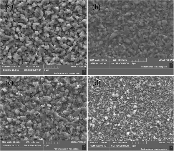
Top view and cross-sectional scanning electron microscopy (SEM) images of the CZTSSe thin films selenized under Ar–Se atmosphere at different temperatures are shown in Fig. 1, and the surface micrograph of the precursor film is presented in Fig. S1.† The CZTS precursor film has a smooth, uniform surface and is consisted of nanocrystalline.10 After selenization, the crystal size enhances significantly and the selenization temperature has a significant impact on the morphology of the CZTSSe absorber, as shown in Fig. 1. The film formed at 500 °C shows a uniform, crack-free, and pinhole-free surface with nanocrystal structure (Fig. 1a). As the selenization temperature increases, the size of grains are enlarged, indicating better crystallinity, while some pores can be observed on the surface (Fig. 1b and c). When the sample is selenized at 580 °C, the film is dense, smooth and pinhole-free with micrometer-sized grains, as shown in Fig. 1d. From the cross-sectional SEM images in the insets, it is shown that when the selenization temperature rises to 560 °C or higher, the grains span the entire film thickness, which is beneficial to the photocarrier transportation and reduce the bulk recombination.
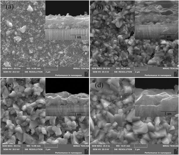 |
| | Fig. 1 Top view SEM images of the CZTSSe thin films annealed under Ar–Se atmosphere at four temperatures of (a) 500 °C, (b) 530 °C, (c) 560 °C and (d) 580 °C for 40 min. Inset: SEM cross-sectional images of the samples. The temperature of Se was always 400 °C under these conditions. The composition of precursor is designed to be Cu/(Zn + Sn) = 0.86 and Zn/Sn = 1.0. | |
As shown in Fig. 2a, the X-ray diffraction (XRD) patterns of the CZTSSe thin film selenized above 500 °C reveal the formation of CZTSSe without Cu or Sn sulfides/selenides secondary phases. The intensity of the (112) main diffraction peaks corresponding to the CZTSSe increases gradually with increasing selenization temperature under 560 °C, and shows a significant boost for the sample selenized at 580 °C. Furthermore, the (101) characteristic peak from CZTSSe is visible at high selenization temperature, implying that the CZTSSe thin film has good crystallinity.16 Raman spectroscopy is also applied to detect the phase purity of the CZTSSe thin films because some binary, ternary sulfides/selenides, such as ZnS, Cu2SnS3, ZnSe and Cu2SnSe3, have similar XRD patterns with CZTS and Cu2ZnSnSe4 (CZTSe).17 Fig. 2b shows the Raman spectra of CZTSSe thin films selenized at different temperatures. For all of the CZTSSe films, the main peaks are located at approximately 200 cm−1 and 330 cm−1, which are consistent with the A1 vibration mode of CZTSe and CZTS, respectively.18 No other sulfides and/or selenides secondary phases are found in the Raman spectra for the CZTSSe thin films. It is obviously observed that with the increase of selenization temperature, the intensity of main peaks increases, indicating that the films obtain better crystallinity. However, the Raman peak intensity significantly decreases at 580 °C due to the degradation of the CZTSSe film. Moreover, the atomic ratio image of the CZTSSe films selenized at different temperatures is shown in Fig. S2.† The change of Cu/(Zn + Sn) ratio at different temperatures is very little, and the Cu/(Zn + Sn) ratio is a bit lower than that of the precursor solution. The Zn/Sn ratios at 500 °C and 530 °C are 0.9, lower than the ratio of the precursor solution. But the Zn/Sn ratio rises to nearly 1.0 at 560 °C, roughly equal to the ratio of the precursor solution. Besides, the S/(S + Se) ratio slightly increases with the rise in selenization temperature, which can also be reflected from Raman spectra in Fig. 2b. For films with intermediate S/Se content, the main peaks from both sulfide and selenide are present, and shift toward one other.9 When the sample is selenized at above 530 °C, the peak at around 200 cm−1 shifts to higher wavenumber direction which is closer to the pure sulfide (338 cm−1) side compared with thin film selenized at 500 °C. From above results, it is evident that the sol–gel and selenization approach allows kesterite CZTSSe fabrication and easy control to phase and microstructure by adjusting selenization temperature. As the temperature increases, the grain size increases gradually. However, when temperature rises to 580 °C, it is difficult for the absorber film to stay stable. Hence, we choose 560 °C as the optimal selenization temperature in this process.
 |
| | Fig. 2 (a) XRD patterns of CZTSSe annealed at 500 °C, 530 °C, 560 °C and 580 °C for 40 min on molybdenum (Mo). (b) The corresponding Raman spectra of the CZTSSe thin films. | |
3.2. Effect of the selenization time
The SEM images in Fig. 3 illustrate an improvement in crystallization and film quality with different selenization times. It is shown that the grain size gradually increases with an increase in selenization time. The film selenized for 40 min is uniform and pinhole-free with micrometer-sized grains. Besides, as shown in the EDS component atomic ratio image (Fig. S3†), metal composition of the thin films selenized for different selenization times have little difference. The ratio of S/(S + Se) keeps steady (about 30%) because the substitution reactions occur spontaneously and fast,13 which demonstrates that with the selenization time increasing, the crystallinity and size of grain increase, but the Se incorporation remains the same.
 |
| | Fig. 3 SEM images of the CZTSSe thin films annealed under Ar–Se atmosphere at 560 °C for (a) 5 min, (b) 20 min, (c) 40 min, and (d) 60 min. | |
In Fig. 4a, XRD patterns demonstrate kesterite structure for absorbers selenized for 5–60 min. A selenium annealing atmosphere makes CZTSSe form as early as 5 min. When selenization time increases, the peak intensities for (112), (220)/(204), (116)/(312) planes become stronger and sharper, and (101) peak belonging to the kesterite structure becomes observable, indicating an improvement in crystallization and film quality, consistent with the SEM results (Fig. 3). In order to detect the presence of possible binary and ternary phases, the Raman scattering is applied again. Fig. 4b shows that the selenide-based (∼200 cm−1) and sulfide-based (∼330 cm−1) Raman peaks are the main peaks, which agree with the literature results,18 and no other impurity phases are observed. Moreover, with the extension of the selenization time, the characteristic peaks sharpen, indicating that the film crystallinity gradually gets better, which is in agreement with the XRD results. The peak intensities have little change after 40 min, therefore, 40 min is chosen as the appropriate selenization time.
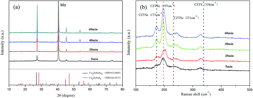 |
| | Fig. 4 (a) XRD patterns of CZTSSe annealed at 560 °C for 5 min, 20 min, 40 min and 60 min on Mo. (b) The corresponding Raman spectra of the CZTSSe thin films. | |
3.3. Effects of the composition
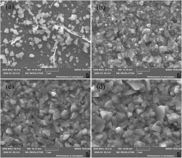
In order to study the influence of the metal component on the morphology and structure of CZTSSe film, the precursor solutions with various Cu/(Zn + Sn) ratios ranging from 0.66 to 0.96 were prepared. Chen et al. reported that acceptors in CZTS are due to Cu vacancies (VCu) and substitution of Cu in Zn site (CuZn). They calculated the acceptor transition energy levels for CuZn and VCu to be 0.10 and 0.02 eV, respectively, which are both above the valence band maximum.19 Since CuZn is a relatively deep acceptor, the shallow acceptor of VCu is effective for improving the efficiency of CZTS solar cells. The Cu-poor composition suppresses CuZn formation and enhances VCu formation.20 As can be seen from Fig. 5, the CZTSSe absorber at Cu/(Zn + Sn) ratio of 0.66 shows uneven morphology with some pores. As the Cu/(Zn + Sn) ratio increases, the CZTSSe thin film tends to be uniform with larger grain size. When the ratio of Cu/(Zn + Sn) rises to 0.86, the grains with size above 1 μm are obtained. Similar phenomenon was reported by Tanaka et al. for the sol–gel prepared CZTS film21 and by G. Suresh Babu et al. for the co-evaporated Cu2ZnSnSe4 thin film.22 However, the film morphology deteriorates obviously with some white clusters on the surface when Cu/(Zn + Sn) ratio is as high as 0.96. In summary, the film obtains the optimal morphology at Cu/(Zn + Sn) ratio of 0.86. Besides, no impurity phases are observed at this Cu/(Zn + Sn) ratio, as seen in Fig. S4.†
 |
| | Fig. 5 SEM images of the surface of the CZTSSe thin films. The Cu/(Zn + Sn) ratios of precursor solutions were (a) 0.66, (b) 0.76, (c) 0.86 and (d) 0.96, respectively. These four films were annealed under selenium atmosphere at 560 °C for 40 min. | |
Related defect theory study for CZTSSe proves that Zn/Sn ratio has a significant impact on intrinsic defects of CZTSSe, which affects the carrier diffusion length and mobility.23 Under Cu-poor condition, the increase of zinc content can promote the formation of [VCu + ZnCu], which can result in band bending that can promote the separation of photo-generated electron–hole pairs and subsequently improve the photoelectric conversion efficiency of the device.23 Here, we investigate the influence of Zn/Sn ratio on the crystallinity in the range of 0.8 to 1.4. Fig. 6 shows SEM images of CZTSSe films with different Zn/Sn ratios. It can be seen that as the Zn/Sn ratio rises from 0.8 to 1.2, the CZTSSe thin film shows a denser surface morphology with larger crystal size. However, some small white grains, which have been previously assigned as ZnS(Se),24 appear on the surface for Zn/Sn ratio of 1.2. When Zn/Sn ratio further increases to 1.4, small white particles almost cover the whole film surface, and the size of grain decreases obviously. Fairbrother et al. interpreted this as ZnSe inhibiting grain growth.24 Therefore, the most proper Zn/Sn ratio is 1.0 from the viewpoint of morphology, which is lower than those described for previous record devices.5,25 The Zn/Sn ratio of 1.0 benefits the formation of SnOx during the post-annealing in air, which is a common process in device fabrication.26 SnOx at the grain boundaries is found to correlate with high device performance and is proposed to passivate GB recombination sites.27 Furthermore, no binary and ternary phases are found at such ratio from Fig. S4.†
 |
| | Fig. 6 Four SEM images of CZTSSe films with Zn/Sn ratios of (a) 0.8, (b) 1.0, (c) 1.2, and (d) 1.4. The selenization temperature of 560 °C, the selenization time of 40 min, and the Cu/(Zn + Sn) ratio of 0.86 were utilised in the synthesis. | |
3.4. Device performance and limited factor
The CZTSSe device synthesized by sol–gel approach under the optimal conditions (as stated above) achieves the highest photoelectric conversion efficiency of 8.08%, in which the ratios of Cu/(Zn + Sn) and Zn/Sn of CZTSSe thin film are ∼0.86 and 1.0, respectively (EDS spectrum shown in Fig. S5†). The electrical characteristics of the best device in the dark and under illumination AM 1.5 are presented in Fig. 7a, without MgF2 antireflection layer. The device produces remarkably high short-circuit current density (Jsc = 32.78 mA cm−2), moderate open-circuit voltage (Voc = 487 mV) and low fill factor (FF = 51%). The series resistance (Rs) is 3.8 Ω cm2, which is somewhat larger than those reported by Mitzi et al. for the best CZTSSe solar cells.28 The low shunt resistance (Rsh = 181.4 Ω cm2) suggests that there may be some shunt paths in the device or a strong voltage-dependent current collection effect. The external quantum efficiency (EQE) curve of the device is shown in Fig. 7b. The optical bandgap of the CZTSSe absorber estimated from the x-axis intercept of [EQE × E]2 vs. E plot in the inset of Fig. 7b is 1.20 eV. Recently Chen et al. calculated the band gap bowing of Cu2ZnSn(SxSe1−x) to be: Eg(x) = xEg(CZTS) + (1 − x)Eg(CZTSe) − bx(1 − x) where b is approximately 0.1 eV.29 The alloy band gap decreases monotonically when the Se content increases, from 1.5 eV at x = 0 to 0.96 eV at x = 1. The decrease is almost linear. From the Fig. S3,† under the optimal condition (the CZTSSe absorber selenized at 560 °C for 40 min, with ratios of Cu/(Zn + Sn) = 0.86 and Zn/Sn = 1.0), the S/(S + Se) ratio is about 0.30. Using x = 0.30, Eg is 1.14 eV, which is very close to the band gap estimated by EQE data. EQE value approaches 90% in the visible range, however the EQE decays in the infrared region, especially beyond 800 nm, due to a short minor carrier lifetime30 and/or a narrow depletion layer.31 From the analyses of electrical characteristics, the largest room for improvement compared with chalcopyrite devices with similar bandgap values is in open-circuit voltage and fill factor.
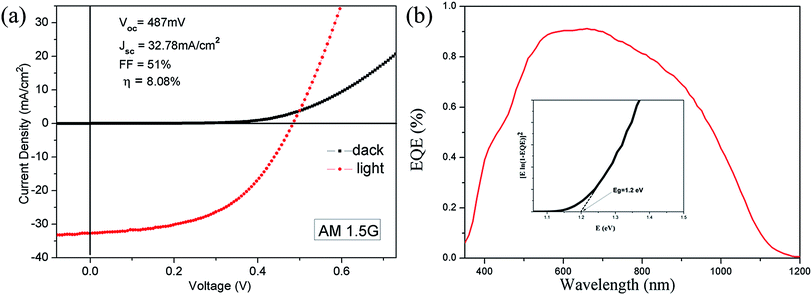 |
| | Fig. 7 (a) I–V characteristics of the 8.08% CZTS solar cell under dark (black solid line) and 1 sun illumination (red dotted line). (b) The quantum efficiency (QE) curve. The inset shows the plot of [EQE × E]2 vs. E to evaluate the band gap. | |
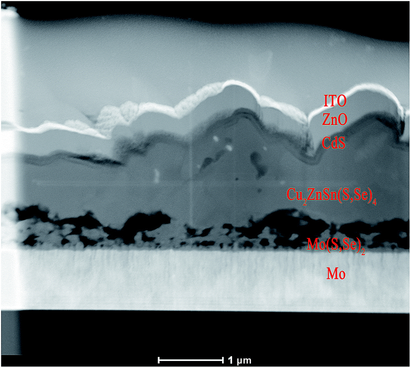
To gain insight into the limiting factors in solar cell efficiency, we investigate section feature and compositional distribution of the CZTSSe device. A cross-sectional scanning transmission electron microscopy (STEM) image of the best device in Fig. 8 shows large grains (∼1.3–1.9 μm) spanning the entire CZTSSe layer. Typical absorption coefficients reported for CZTSSe thin films are around 105 cm−1, which suggests that a thicker absorber is needed to effectively absorb the solar spectrum and reduce recombination at the back contact.32,33 It is evident that the film thickness is not uniform with many thinner regions, which may be considered to be one of the important reasons for low shunt resistance and low Voc. The presence of large pores and voids is also clearly observable in the bottom of CZTSSe film, which is the primary cause of a high series resistance and a low fill factor. In Fig. 9a, an energy-dispersive X-ray spectroscopy (EDX) line scan longitudinally through the device shows uniform elemental distribution. As it is evident in this figure and also noted in other reports,34,35 a detectable amount of copper is observed in the Mo(S,Se)2 layer. In addition, a moderate thickness Mo(S,Se)2 layer (∼200 nm) is observed between the Mo substrate and CZTSSe absorber, as thick as devices with efficiency beyond 10%,28,35 but the Mo(S,Se)2 layer is still thicker than the optimal thickness of 50 nm from numerical analysis.36 A thick Mo(S,Se)2 can result in the increase in Rs and subsequently decrease in FF.37 There have been many methods to inhibit Mo(S,Se)2 formation such as an intermediate layer,38–41 other alternative back contact materials42 and a prealloying process.43 EDX compositional profilings laterally across the absorber are shown in Fig. 9b, which demonstrates that copper, zinc and tin concentrations stay basically constant and further confirms that the S/(S + Se) ratio is about 0.30. However, some obvious fluctuations in S/(S + Se) ratio are also observed. Previous research on CIGSe has shown that relatively small fluctuations of band gap can lead to a drastic decrease of the device efficiency, and the higher the voltage at the cell, the smaller are the fluctuations.44 The low Voc can presumably be caused by the effect of band gap fluctuations resulting from the inhomogeneous distribution of Se.
 |
| | Fig. 8 Cross-sectional STEM image of the 8.08% CZTSSe device. | |
 |
| | Fig. 9 EDX analysis on the 8.08% CZTSSe device: (a) across the thickness of the device and (b) laterally across the CZTSSe layer. The red arrow in the inset demonstrates the direction of the EDX scanning. Quantitative analysis for S and Mo in the thin film is not feasible due to the similar spectral peak in the EDX analysis. Scanning range from 2900 to 3800 nm in (a) is considered as Mo layer, in accordance with the sputtering thickness of Mo. | |
4. Conclusion
Here we synthesized CZTSSe thin film solar cell by sol–gel method which is a simple and facile solution method using commercially available precursors and non-toxic solvents. We investigated the influence of selenization temperature, selenization time and metal compositions on morphology and phase of the films. The CZTSSe absorber selenized at 560 °C for 40 min, with ratios of Cu/(Zn + Sn) = 0.86 and Zn/Sn = 1.0, achieves a uniform and pinhole-free surface morphology. Moreover, XRD and Raman analyses reveal that no other impurity phases are observed under such condition. A power conversion efficiency (PCE) of 8.08% (active cell area) has been achieved. However, the present CZTSSe device still suffers from some problems of voids at the back contact, a thick Mo(S,Se)2 layer, nonuniform film thickness and inhomogeneous distribution of Se. The PCE could be further enhanced by the optimization of the back contact and homogeneity of chalcogen components. In addition, multivariate chemometrics approach45,46 will be applied to take into account all the relevant variables and their interactions, finding the best experimental conditions for the proper functioning of the CZTSSe thin films in the future.
Acknowledgements
This work was supported by the National Natural Science Foundation of China (Grant no. 51222403 and 51272292), Doctoral Fund of Ministry of Education of China (20110162110050) and Hunan Provincial Natural Science Foundation of China (13JJ1003).
References
- J. J. Scragg, P. J. Dale, L. M. Peter, G. Zoppi and I. Forbes, Phys. Status Solidi B, 2008, 245, 1772–1778 CrossRef CAS.
- H. Katagiri, K. Jimbo, W. S. Maw, K. Oishi, M. Yamazaki, H. Araki and A. Takeuchi, Thin Solid Films, 2009, 517, 2455–2460 CrossRef CAS.
- K. Ito and T. Nakazawa, Jpn. J. Appl. Phys., 1988, 27, 2094–2097 CrossRef CAS.
- J. Krustok, R. Josepson, M. Danilson and D. Meissner, Sol. Energy, 2010, 84, 379–383 CrossRef CAS.
- J. Kim, H. Hiroi, T. K. Todorov, O. Gunawan, M. Kuwahara, T. Gokmen, D. Nair, M. Hopstaken, B. Shin, Y. S. Lee, W. Wang, H. Sugimoto and D. B. Mitzi, Adv. Mater., 2014, 26, 7427–7431 CrossRef CAS PubMed.
- K. Wang, O. Gunawan, T. Todorov, B. Shin, S. J. Chey, N. A. Bojarczuk, D. Mitzi and S. Guha, Appl. Phys. Lett., 2010, 97, 143508 CrossRef.
- T. P. Dhakal, C. Peng, R. Reid Tobias, R. Dasharathy and C. R. Westgate, Sol. Energy, 2014, 100, 23–30 CrossRef CAS.
- S. Ahmed, K. B. Reuter, O. Gunawan, L. Guo, L. T. Romankiw and H. Deligianni, Adv. Energy Mater., 2012, 2, 253–259 CrossRef CAS.
- W. Yang, H.-S. Duan, B. Bob, H. Zhou, B. Lei, C.-H. Chung, S.-H. Li, W. W. Hou and Y. Yang, Adv. Mater., 2012, 24, 6323–6329 CrossRef CAS PubMed.
- Z. Su, K. Sun, Z. Han, H. Cui, F. Liu, Y. Lai, J. Li, X. Hao, Y. Liu and M. A. Green, J. Mater. Chem. A, 2014, 2, 500–509 CAS.
- K. Zhang, Z. Su, L. Zhao, C. Yan, F. Liu, H. Cui, X. Hao and Y. Liu, Appl. Phys. Lett., 2014, 104, 141101 CrossRef.
- Y. Wenbing, D. Hsin-Sheng, B. Bob, L. Bao, L. Sheng-Han and Y. Yang, Adv. Mater., 2012, 24, 6323–6329 CrossRef PubMed.
- J. Li, Y. Zhang, H. Wang, L. Wu, J. Wang, W. Liu, Z. Zhou, Q. He and Y. Sun, Sol. Energy Mater. Sol. Cells, 2015, 132, 363–371 CrossRef CAS.
- F. Liu, Y. Lai, J. Liu, B. Wang, S. Kuang, Z. Zhang, J. Li and Y. Liu, J. Alloys Compd., 2010, 493, 305–308 CrossRef CAS.
- F. Liu, F. Zeng, N. Song, L. Jiang, Z. Han, Z. Su, C. Yan, X. Wen, X. Hao and Y. Liu, ACS Appl. Mater. Interfaces, 2015, 7, 14376–14383 CAS.
- G. Feng, M. Tsuyoshi and W. Takahiro, Jpn. J. Appl. Phys., 2014, 53, 04ER11 CrossRef.
- W. M. Hlaing Oo, J. L. Johnson, A. Bhatia, E. A. Lund, M. M. Nowell and M. A. Scarpulla, J. Electron. Mater., 2011, 40, 2214–2221 CrossRef CAS.
- D. B. Mitzi, O. Gunawan, T. K. Todorov, K. Wang and S. Guha, Sol. Energy Mater. Sol. Cells, 2011, 95, 1421–1436 CrossRef CAS.
- S. Chen, X. G. Gong, A. Walsh and S.-H. Wei, Appl. Phys. Lett., 2010, 96, 021902 CrossRef.
- K. Tanaka, Y. Fukui, N. Moritake and H. Uchiki, Sol. Energy Mater. Sol. Cells, 2011, 95, 838–842 CrossRef CAS.
- K. Tanaka, Y. Fukui, N. Moritake and H. Uchiki, Sol. Energy Mater. Sol. Cells, 2011, 95, 838–842 CrossRef CAS.
- G. Suresh Babu, Y. B. Kishore Kumar, P. Uday Bhaskar and S. Raja Vanjari, Sol. Energy Mater. Sol. Cells, 2010, 94, 221–226 CrossRef CAS.
- S. Chen, A. Walsh, X.-G. Gong and S.-H. Wei, Adv. Mater., 2013, 25, 1522–1539 CrossRef CAS PubMed.
- A. Fairbrother, X. Fontané, V. Izquierdo-Roca, M. Placidi, D. Sylla, M. Espindola-Rodriguez, S. López-Mariño, F. A. Pulgarín, O. Vigil-Galán and A. Pérez-Rodríguez, Prog. Photovoltaics, 2014, 22, 479–487 CAS.
- N. Song, Y. Wang, Y. Hu, Y. Huang, W. Li, S. Huang and X. Hao, Appl. Phys. Lett., 2014, 104, 092103 CrossRef.
- Q. Guo, G. M. Ford, W.-C. Yang, B. C. Walker, E. A. Stach, H. W. Hillhouse and R. Agrawal, J. Am. Chem. Soc., 2010, 132, 17384–17386 CrossRef CAS PubMed.
- K. Sardashti, R. Haight, T. Gokmen, W. Wang, L.-Y. Chang, D. B. Mitzi and A. C. Kummel, Adv. Energy Mater., 2015, 1402180, DOI:10.1002/aenm.201402180.
- T. K. Todorov, J. Tang, S. Bag, O. Gunawan, T. Gokmen, Y. Zhu and D. B. Mitzi, Adv. Energy Mater., 2013, 3, 34–38 CrossRef CAS.
- S. Chen, A. Walsh, J.-H. Yang, X. G. Gong, L. Sun, P.-X. Yang, J.-H. Chu and S.-H. Wei, Phys. Rev. B: Condens. Matter Mater. Phys., 2011, 83, 245202 CrossRef.
- W. Ki and H. W. Hillhouse, Adv. Energy Mater., 2011, 1, 732–735 CrossRef CAS.
- B. Shin, O. Gunawan, Y. Zhu, N. A. Bojarczuk, S. J. Chey and S. Guha, Prog. Photovoltaics, 2013, 21, 72–76 Search PubMed.
- J.-S. Seol, S.-Y. Lee, J.-C. Lee, H.-D. Nam and K.-H. Kim, Sol. Energy Mater. Sol. Cells, 2003, 75, 155–162 CrossRef CAS.
- Q. Guo, G. M. Ford, W.-C. Yang, B. C. Walker, E. A. Stach, H. W. Hillhouse and R. Agrawal, J. Am. Chem. Soc., 2010, 132, 17384–17386 CrossRef CAS PubMed.
- S. Bag, O. Gunawan, T. Gokmen, Y. Zhu, T. K. Todorov and D. B. Mitzi, Energy Environ. Sci., 2012, 5, 7060–7065 CAS.
- W. Wang, M. T. Winkler, O. Gunawan, T. Gokmen, T. K. Todorov, Y. Zhu and D. B. Mitzi, Adv. Energy Mater., 2014, 4, 1301465 Search PubMed.
- P. Chelvanathan, M. I. Hossain, J. Husna, M. Alghoul, K. Sopian and N. Amin, Jpn. J. Appl. Phys., 2012, 51, 10NC32 CrossRef.
- K.-J. Yang, J.-H. Sim, B. Jeon, D.-H. Son, D.-H. Kim, S.-J. Sung, D.-K. Hwang, S. Song, D. B. Khadka, J. Kim and J.-K. Kang, Prog. Photovoltaics, 2015, 23, 862–873 CAS.
- H. Cui, X. Liu, F. Liu, X. Hao, N. Song and C. Yan, Appl. Phys. Lett., 2014, 104, 041115 CrossRef.
- W. Li, J. Chen, H. Cui, F. Liu and X. Hao, Mater. Lett., 2014, 130, 87–90 CrossRef CAS.
- F. Liu, K. Sun, W. Li, C. Yan, H. Cui, L. Jiang, X. Hao and M. A. Green, Appl. Phys. Lett., 2014, 104, 051105 CrossRef.
- F. Zhou, F. Zeng, X. Liu, F. Liu, N. Song, C. Yan, A. Pu, J. Park, K. Sun and X. Hao, ACS Appl. Mater. Interfaces, 2015, 7, 22868–22873 CAS.
- G. Altamura, L. Grenet, C. Roger, F. Roux, V. Reita, R. Fillon, H. Fournier, S. Perraud and H. Mariette, J. Renewable Sustainable Energy, 2014, 6, 011401 CrossRef.
- J. Li, Y. Zhang, W. Zhao, D. Nam, H. Cheong, L. Wu, Z. Zhou and Y. Sun, Adv. Energy Mater., 2015, 5, 1402178 Search PubMed.
- J. H. Werner, J. Mattheis and U. Rau, Thin Solid Films, 2005, 480–481, 399–409 CrossRef CAS.
- F. Bella, M. Imperiyka and A. Ahmad, J. Photochem. Photobiol., A, 2014, 289, 73–80 CrossRef CAS.
- H. Sun and R. Dixon, J. Power Sources, 2014, 272, 404–414 CrossRef CAS.
Footnote |
| † Electronic supplementary information (ESI) available. See DOI: 10.1039/c5ra18975f |
|
| This journal is © The Royal Society of Chemistry 2016 |
Click here to see how this site uses Cookies. View our privacy policy here.