
Au@ZnO core–shell nanostructures with plasmon-induced visible-light photocatalytic and photoelectrochemical properties†
Xiankun
Shao
,
Benxia
Li
*,
Baoshan
Zhang
,
Liangzhi
Shao
and
Yongmeng
Wu
School of Materials Science and Engineering, Anhui University of Science and Technology, Huainan, Anhui 232001, China. E-mail: libx@mail.ustc.edu.cn; Fax: +86-554-6668643; Tel: +86-554-6668649
First published on 18th April 2016
Abstract
Constructing a core–shell nanostructured photocatalyst by integration of plasmonic metal nanocrystals and a semiconductor can offer large active metal/semiconductor interfacial areas and avoid aggregation of the metal nanocrystals. Herein, well-defined Au@ZnO core–shell nanostructures were prepared by coating ZnO on cetyltrimethylammonium bromide (CTAB) stabilized Au nanospheres in aqueous solution. The resultant core–shell nanostructures have Au-nanosphere cores with a diameter of ∼55 nm and ZnO shells with a thickness of ∼50 nm. After calcination at 350 °C in air, the mesoporous ZnO shell with higher crystallinity and a larger surface area was obtained without any significant change in the morphology or plasmon band of Au@ZnO. The specific surface plasmon resonance of the Au-nanosphere cores endows the Au@ZnO nanostructures with strong visible light absorption around 550 nm. The photocatalytic degradation of an organic pollutant was performed under simulated sunlight and monochromatic LED light with three different wavelengths (365 nm, 520 nm, 660 nm), demonstrating the enhanced photocatalysis of the Au@ZnO nanostructures. Furthermore, the Au@ZnO as a photoelectrode material presents a higher photocurrent density than that of pure ZnO nanoparticles under simulated sunlight. The electrochemical impedance spectra (EIS) Nyquist plots also confirm the higher charge transfer efficiency of the Au@ZnO nanostructures. Such plasmonic metal–semiconductor core–shell nanostructures would provide a desirable platform for studying plasmon-induced/enhanced processes and have great potential in light-harvesting applications.
Introduction
Development of renewable energy harvesting methods and working towards a sustainable environment are two major challenges facing humanity currently. The semiconductor photocatalysis technique has received much attention as it is deemed to be one of the potential solutions for solar energy conversion and counteracting environmental deterioration.1–4 There are three key factors required for far more efficient solar energy conversion, including maximized photon absorption, efficient charge separation (minimal recombination), and finally effective utilization of these separated charges.5,6 The prerequisite for more efficient solar energy conversion and utilization via the photocatalysis technique is the development of photocatalysts with new and improved properties.7–9 A convenient and efficient strategy to design and engineer photocatalysts with optimized performance in terms of highly efficient solar energy conversion is the integration of available materials with synergistic properties.10,11Gold nanocrystals have shown significant promise in visible-light harvesting in the photocatalytic process due to their specific surface plasmon resonance (SPR) properties.12–14 It has been demonstrated that incorporating Au nanocrystals into semiconductor nanostructures could achieve a collective effect to greatly increase the efficiency of photocatalytic processes, including water splitting,15 organic compound decomposition,16 photosynthesis of organic molecules,17 and photocatalytic reduction of carbon dioxide.18,19 Constructing a heterostructure of Au nanocrystals and a semiconductor can often facilitate charge separation upon the generation of electron/hole pairs through photon excitation in the semiconductor, because the Fermi levels of noble metals are typically lower than the conduction band edges of usual semiconductor photocatalysts.20–22 Furthermore, Au nanocrystals can broaden and enhance the light absorption of semiconductors through scattering, absorption enhancement, and sensitization, because they have extremely large absorption/scattering cross-sections and can strongly focus light close to their surface.23,24 As a result, some attempts have been made to improve the photocatalytic performance by fabricating Au/semiconductor hybrid nanostructures.25,26 Among them, loading of Au nanoparticles over the semiconductor surface is a common method.27–30 However, Au nanoparticles deposited on the surface of semiconductors reduce the active surface area involved in photocatalytic reactions, and also tend to aggregate and be chemically corroded. To overcome these problems, an alternative option is to construct Au@semiconductor core–shell nanostructures.31 The core–shell nanostructures not only protect the Au nanocrystal core from aggregation and chemical corrosion during reaction under harsh conditions, but also provide a maximized and intimate interface between Au and the semiconductor, which is of significance for the plasmon–exciton interactions and charge transfer.32–35 Most of the reported studies were performed on the noble-metal@TiO2 core–shell nanostructures for photocatalytic applications because of the high popularity of TiO2 as a photocatalyst.35–38 However, the research on exploiting such core–shell nanostructured photocatalysts comprising other semiconductors needs to be paid more attention.
Among various semiconductors, zinc oxide (ZnO), a well-known n-type semiconductor with a direct wide band gap of 3.37 eV, has been receiving considerable attention in many potential applications including photocatalysts, field effect transistors, solar cells, chemical sensors, and so on.39–42 ZnO has a conduction band edge located at approximately the same level as that of TiO2. More attractively, the electron mobility of ZnO has been proven to be higher than that of TiO2.43 Although a large number of studies have been conducted on the synthesis and photocatalytic properties of various ZnO nanostructures,20,44 the solar-driven photocatalytic efficiency remains very low because of the fast recombination of the photo-excited electron–hole pairs in the single phase semiconductor and its responsiveness only to ultraviolet light. The intimate integration of Au nanocrystals and ZnO nanostructures will endow them with a high visible-light-harvesting ability. Furthermore, combining the plasmonic Au nanocrystals with ZnO in a well-defined core–shell nanostructure will be highly desirable to better understand the light absorption, charge carrier excitation and transfer in the promotion of solar energy conversion. Such an understanding will be helpful for further engineering novel nanostructures with optimal photocatalytic activities.
Inspired by the above ideas, we prepared well-defined Au@ZnO core–shell nanostructures by coating ZnO on CTAB-stabilized Au nanospheres in aqueous solution. After calcination at 350 °C in air, the mesoporous ZnO shell with higher crystallinity and a larger surface area formed without any significant change in the morphology or the SPR band of Au@ZnO nanostructures. The photocatalytic performance was tested under simulated sunlight and monochromatic LED light (365 nm, 520 nm, and 660 nm). Besides, as a photoelectrode material, the Au@ZnO presented a higher photocurrent density than that of the pure ZnO nanoparticles. The electrochemical impedance spectra (EIS) Nyquist plots also confirmed the higher charge transfer efficiency of the Au@ZnO nanostructures.
Experimental section
Synthesis
For comparison, the pure ZnO nanoparticles were also prepared under the same conditions without adding Au nanospheres. Moreover, Au@SiO2 core–shell nanostructures which have the same Au-nanosphere cores as those of the Au@ZnO sample were also prepared using a reported method.46 The detailed procedures for preparing the Au@SiO2 sample are described in the ESI.†
Characterization
The X-ray diffraction (XRD) patterns were recorded on a Japan Shimadzu XRD-6000 with graphite monochromatized high-intensity CuKα radiation (λ = 1.542 Å), and operated at 40 kV voltage and 30 mA current. The field emission scanning electron microscopy (FESEM) images were obtained on a JEOL JSM-6700F (Japan) at an accelerating voltage of 20 kV. Transmission electron microscopy (TEM) and high-resolution transmission electron microscopy (HRTEM) imaging, scanning transmission electron microscopy (STEM) characterization, and elemental mapping were carried out on a TEM JEOL-2010 (Japan) equipped with an energy dispersive X-ray (EDX) spectrometer. The SEM-EDX mapping was recorded on a FESEM (JEOL JSM-7800, Japan) equipped with an EDX spectrometer. Brunauer–Emmett–Teller (BET) nitrogen adsorption/desorption isotherms and Barrett–Joyner–Halenda (BJH) pore size distributions were measured using a Quantachrome NOVA2000e analyzer (Quantachrome Instruments Corp., USA). The atomic force microscopy (AFM) images were recorded on an AFM (Bruker instrument, Innova1B3BE) operated at room temperature. The UV-visible absorption spectra of the samples were recorded on a Shimadzu UV-2600 UV-visible spectrophotometer, by dispersing the nanoparticles in deionized water.Photocatalytic degradation of RhB under simulated sunlight
The photocatalytic performance of the Au@ZnO core–shell nanostructures was evaluated by the photocatalytic degradation of rhodamine B (RhB) in an aqueous solution under simulated sunlight. The simulated sunlight was provided using a 300 W Xe lamp (CEL-HXF300, Beijing China Education Au-light Co., Ltd). The light source was positioned at about 10 cm from the top of the beaker containing 25 mL of RhB aqueous solution (2 × 10⁻⁵ mol L−1). The optical power density on the reaction solution is measured to be ∼72.66 mW cm−2. Each of the photocatalyst (∼3 mg) was dispersed into the RhB aqueous solution at room temperature in air. Before the light was turned on, the suspension was continuously stirred for 2 h in the dark to achieve an adsorption–desorption equilibrium between the photocatalyst and the dye molecules. The concentration of RhB during the degradation process was monitored using a UV–visible spectrophotometer (Shimadzu UV-2600).Photocatalytic degradation of RhB under monochromatic LED light
The light-emitting diodes (CEL-LED, Beijing China Education Au-light Co., Ltd) provided the continuous monochromatic light source with three different wavelengths of 365 nm, 520 nm, and 660 nm, respectively. The light intensity was ∼15 mW. Because the LED light spot size is very small (∼2.5 cm2), the photocatalytic reactions were carried out in a transparent Pyrex test tube having an inner diameter of 1.5 cm and a length of 12 cm, containing 2 mL of RhB aqueous solution (2 × 10⁻⁵ mol L−1) and ∼0.24 mg of the photocatalyst.Photoelectrochemical tests
Photocurrent measurements were performed using a three-electrode configuration, with the calcined Au@ZnO core–shell nanostructures or the calcined ZnO nanoparticles as the working electrode material, saturated Ag/AgCl as the reference electrode, and a platinum wire as the counter electrode. The electrolyte is KOH aqueous solution (1.0 M). For preparing the working electrode, an indium tin oxide (ITO) glass (2 × 4 cm) was firstly ultrasonically cleaned with a detergent for 30 min, washed with ultrapure water, and then boiled for 1 h in an aqueous solution of hydrogen peroxide (30 mL), ammonium hydroxide (30 mL) and ultrapure water (180 mL). The ITO glass was soaked in ethanol for use after the final washing with ultrapure water. Before use, the ITO glass was further sterilized with 254 nm UV light irradiation. About 3 mg of the sample was dispersed in 0.5 mL of ethanol and then spin-coated on the ITO glass. After natural drying in air for 12 h, the catalyst film on ITO glass was dried at 120 °C for 5 h, and finally used as the working electrode. The current–voltage (I–V) characteristics of the electrode were measured by using an electrochemical workstation (CHI 660D, Shanghai Chenhua, China). The simulated sunlight irradiation is the same as that used in the photocatalytic degradation of RhB. Before photocurrent measurements, the electrolyte was purged with N2 for 1 h to remove the oxygen in the electrolyte. Impedance measurements were performed under illumination in 0.05 M Na2SO4 solution at an open circuit voltage.Results and discussion
In the present work, monodispersed Au nanospheres stabilized with CTAB in aqueous solution were used as the cores to prepare the Au@ZnO core–shell nanostructures via ascorbic acid (AA) induced deposition of the ZnO shell,47 as shown in Fig. 1a. For coating the ZnO shell, Zn(NO3)2, HMT, and a small amount of AA were successively added to the CTAB-stabilized Au nanosphere solution, where AA and Zn2+ could form AA–Zn(II) complex ions due to the polyhydroxy acid structure of AA. The negatively charged AA–Zn(II) complex ions are readily adsorbed on the positively charged surface of the Au nanospheres that are stabilized by CTA+.48,49 Upon heating at 90 °C, HMT decomposed to release OH− and increased the pH value of the solution, which promoted the deposition of ZnO on the Au nanosphere surface. Before coating the ZnO shell, the monodispersed Au nanospheres have an average diameter of 55 nm (Fig. 1c and d). In aqueous solution, the nanospheres have ensemble plasmon peaks at 530 nm (Fig. 1b). After coating ZnO, the plasmon peak red shifts to 550 nm, which is attributed to the increase in the refractive index of the surrounding medium.50 The as-prepared Au@ZnO core–shell nanostructures (Fig. 1e and f) present a uniform spherical shape and monodispersing characteristic. The shape of the core–shell nanostructures resembles that of the Au nanosphere cores except that the overall sizes become larger. The TEM image clearly reveals the core–shell structure of this sample, and the thickness of the ZnO shell is about 50 nm.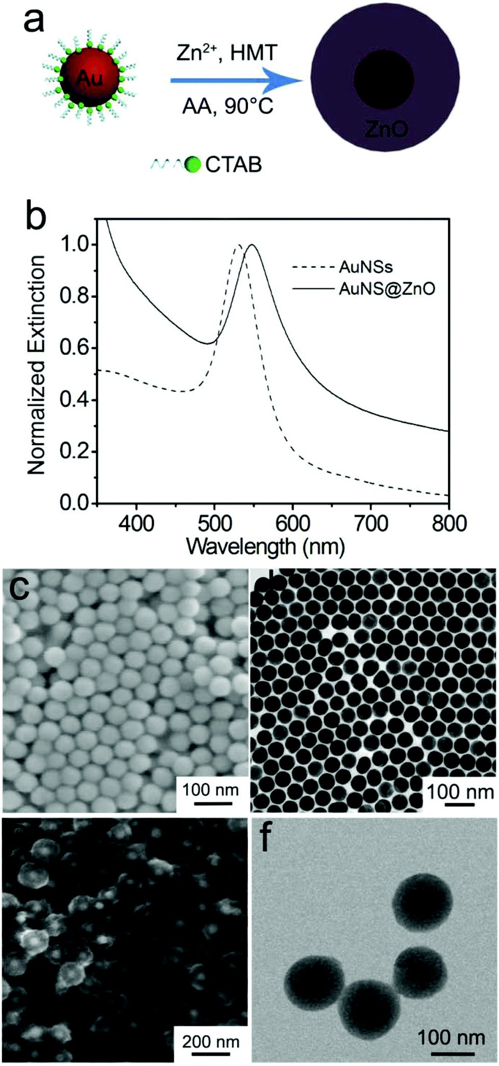 | ||
| Fig. 1 (a) Schematic illustration of the preparation of Au@ZnO core–shell nanostructures. (b) Normalized extinction spectra of the bare Au nanospheres and the Au@ZnO core–shell nanostructures. (c, d) SEM and TEM images of the bare Au nanospheres. (e, f) SEM and TEM images of the Au@ZnO core–shell nanostructures before calcination. | ||
The structure and composition of the as-prepared Au@ZnO sample before calcination were characterized by obtaining the HRTEM image and EDX mapping of a single nanoparticle, as shown in Fig. 2. The interface between the Au-nanosphere core and ZnO shell can be clearly observed in Fig. 2a. The HRTEM image (Fig. 2b) confirms that the ZnO shell is composed of many ZnO nanocrystallines with a size of ∼3 nm. The lattice spacing can be measured to be 0.26 nm, corresponding to the (002) plane of the cubic ZnO phase. The lattice fringe image appears a little obscure because of the poor crystallinity of the ZnO shell and the existence of CTAB molecules in the ZnO shell before calcination. The distribution of elements in the core–shell nanostructures was further confirmed by the elemental mapping of Au, Zn, O and C in a single Au@ZnO core–shell nanostructure (Fig. 2c–f). It can be seen that the Au element was mainly detected in the core region and seldom in the shell region, while the elements Zn and O were probed around the Au core. The C element was from the CTAB molecules adsorbed on the ZnO shell. The distributions of these elements in the core–shell nanostructures are in good agreement with the structure of the Au@ZnO sample.
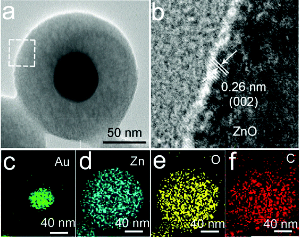 | ||
| Fig. 2 Structure and composition of the Au@ZnO core–shell nanostructure before calcination. (a) TEM image of a single core–shell nanostructure. (b) HRTEM image recorded on the area marked with a white square in (a). (c–f) Elemental distributions of Au, Zn, O and C in the Au@ZnO core–shell nanostructure. | ||
To remove the CTAB molecules adsorbed on the ZnO shell, the as-prepared Au@ZnO sample was calcined at 350 °C for 3 h. The surface morphology and element distributions of the calcined Au@ZnO sample were observed by SEM-EDX mapping (Fig. 3). The SEM image (Fig. 3a) illustrates a large scale of spherical nanoparticles with a size of ∼150 nm. These nanoparticles distribute uniformly and have no reunion. The EDX mappings (Fig. 3b–d) recorded in the whole SEM image indicate that Au, Zn and O elements distribute very uniformly. The three element distributions coincide with those in the Au@ZnO core–shell nanostructures on the whole. The phase compositions of the calcined Au@ZnO core–shell nanostructures were characterized by powder X-ray diffraction (XRD), and compared with the pure ZnO nanoparticles (Fig. S1, ESI†), as shown in Fig. 4a. The diffraction peaks of Au@ZnO are weak but clearly visible. Two sets of the diffraction peaks were observed in the XRD pattern of the Au@ZnO sample, which can be indexed to that of the cubic Au phase (JCPDS no. 04-784) and the cubic ZnO phase (JCPDS no. 36-1451), respectively. The TEM image (Fig. 4b) shows that the calcined Au@ZnO sample remains the core–shell nanostructures although a slight agglomeration occurs. The crystalline grains in the ZnO shell grow larger and their crystallinity increases. The ZnO shells appear rougher and their mesoporous structures are more obvious. In the HRTEM image of a calcined Au@ZnO core–shell nanostructure (Fig. 4c), the lattice spacings of 0.26 and 0.28 nm correspond to the (002) and (100) planes of the cubic ZnO, respectively. The lattice spacing of the Au core was not observed due to the covering of the ZnO shell. In the UV-Vis extinction spectrum of the calcined Au@ZnO core–shell nanostructures (Fig. 5), the plasmon peak of the Au core is located at 570 nm, and the absorption edge of the ZnO shell is at ∼370 nm. The dual absorption of light would be helpful to enhance the sunlight-harvesting ability of the photocatalyst.
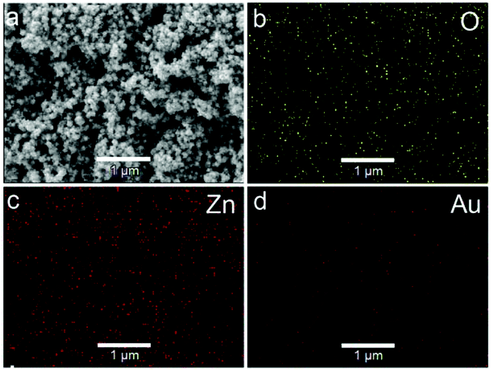 | ||
| Fig. 3 SEM-EDX elemental mapping of the Au@ZnO sample after calcination. (a) SEM image, (b–d) elemental distributions of O, Zn, and Au in the sample. | ||
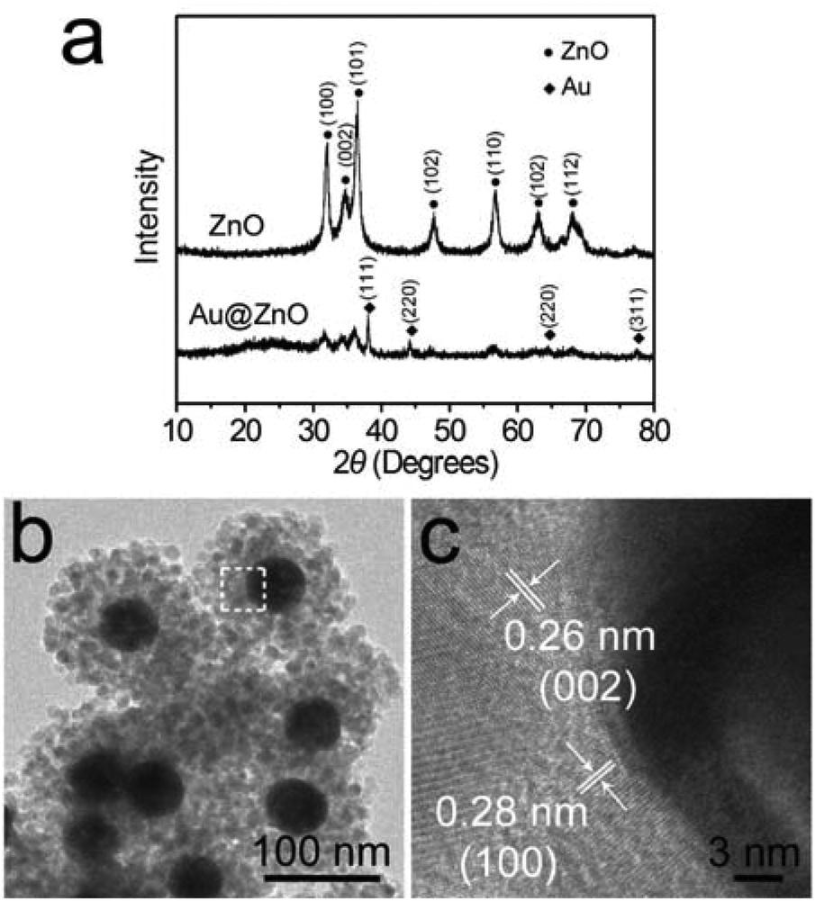 | ||
| Fig. 4 (a) XRD patterns of the calcined Au@ZnO core–shell nanostructures and the calcined pure ZnO nanoparticles. (b) TEM image of the calcined Au@ZnO core–shell nanostructures. (c) HRTEM image recorded from the area marked with a white square in (b). | ||
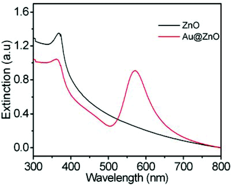 | ||
| Fig. 5 Extinction spectra of the ZnO nanoparticles and the Au@ZnO core–shell nanostructures after calcination. | ||
The specific surface areas and mesoporous features of both the calcined Au@ZnO core–shell nanostructures and the calcined ZnO nanoparticles were characterized by the nitrogen adsorption–desorption process at 77 K, respectively, as shown in Fig. 6 and Table 1. The calcined Au@ZnO sample presents a type IV isotherm (Fig. 6a), which is characteristic of mesoporous materials. The BET surface areas of the two samples were calculated according to the nitrogen desorption isotherms. The BJH mesopore sizes were determined from the nitrogen desorption branches, and the pore volumes were obtained from the cumulative volume of pores between 1.0 nm and 100 nm. The results are listed in Table 1. The calcined Au@ZnO nanostructures present a much larger specific surface area of 153.30 m2 g−1 and a pore volume of 0.23 cm3 g−1, compared with those of the calcined ZnO nanoparticles. The pore diameters in the Au@ZnO nanostructures are around 5.05 nm. The results indicate that the special mesoporous structure of the ZnO shell makes the Au@ZnO core–shell nanostructures have a higher specific surface area and pore volume. So, the core–shell nanostructures have a great advantage in preventing the nanoparticle conglomeration and pore collapse during the calcination process. Therefore, constructing the metal@semiconductor core–shell nanostructures can not only avoid aggregation of the metal nanocrystals and increase the metal/semiconductor interfacial area, but also offer a large active surface area of the semiconductor shell.
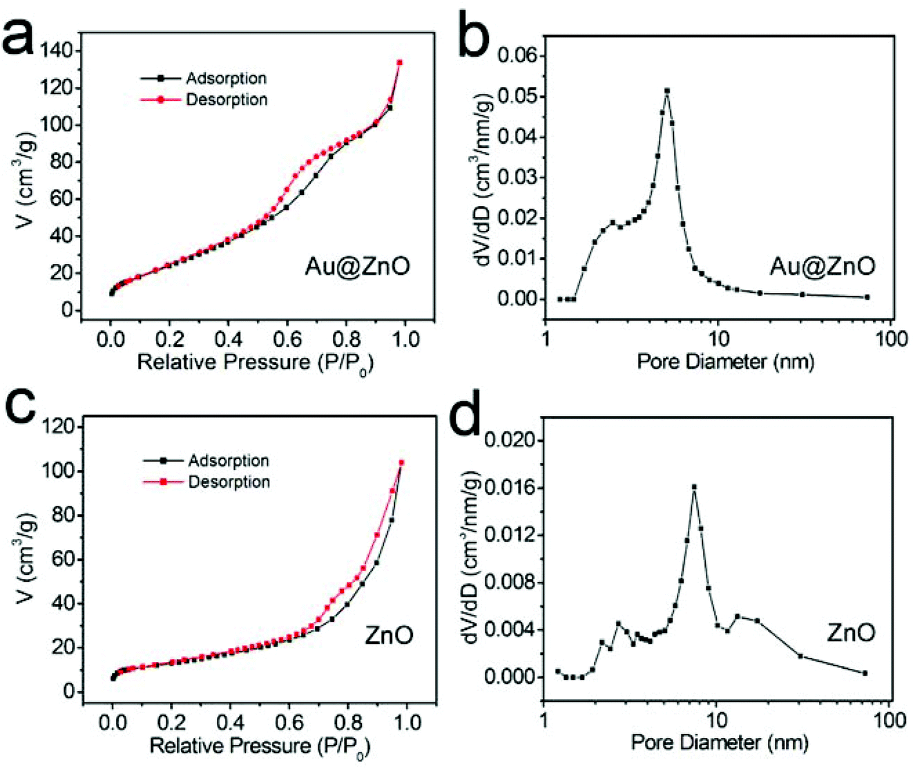 | ||
| Fig. 6 (a, c) Nitrogen adsorption–desorption isotherm plots and (b, d) pore size distributions of Au@ZnO core–shell nanostructures (a, b) and pure ZnO nanoparticles (c, d) after calcination. | ||
| Photocatalyst | Surface areaa (m2 g−1) | Pore sizeb (nm) | Pore volumec (cm3 g−1) |
|---|---|---|---|
| a BET surface areas determined from the nitrogen desorption isotherm measurements. b BJH pore diameters determined from the nitrogen desorption branches. c BJH desorption cumulative volume of pores between 1.0 nm and 100 nm wide. | |||
| Au@ZnO | 153.30 | 5.05 | 0.23 |
| ZnO | 56.60 | 7.46 | 0.16 |
The photocatalytic activity of the calcined Au@ZnO nanostructures was firstly evaluated by degradation of RhB under simulated sunlight irradiation, and the results are shown in Fig. 7. The Au@ZnO sample shows the highest photocatalytic activity among several different photocatalysts. The bare Au nanospheres and the Au@SiO2 core–shell nanostructures (Fig. S2, ESI†) exhibit hardly any photocatalytic activity for RhB degradation. The kinetic linear fitting results (Fig. 7c) reveal that the kinetic data of the photocatalytic degradation of RhB match the first-order reaction kinetics model well. The reaction rate constant (k) values corresponding to various photocatalysts are summarized visually by a histogram in Fig. 7d. Specifically, the reaction rate constant catalyzed by the Au@ZnO catalyst is 5.5-fold of that of the reaction catalyzed by the pure ZnO catalyst.
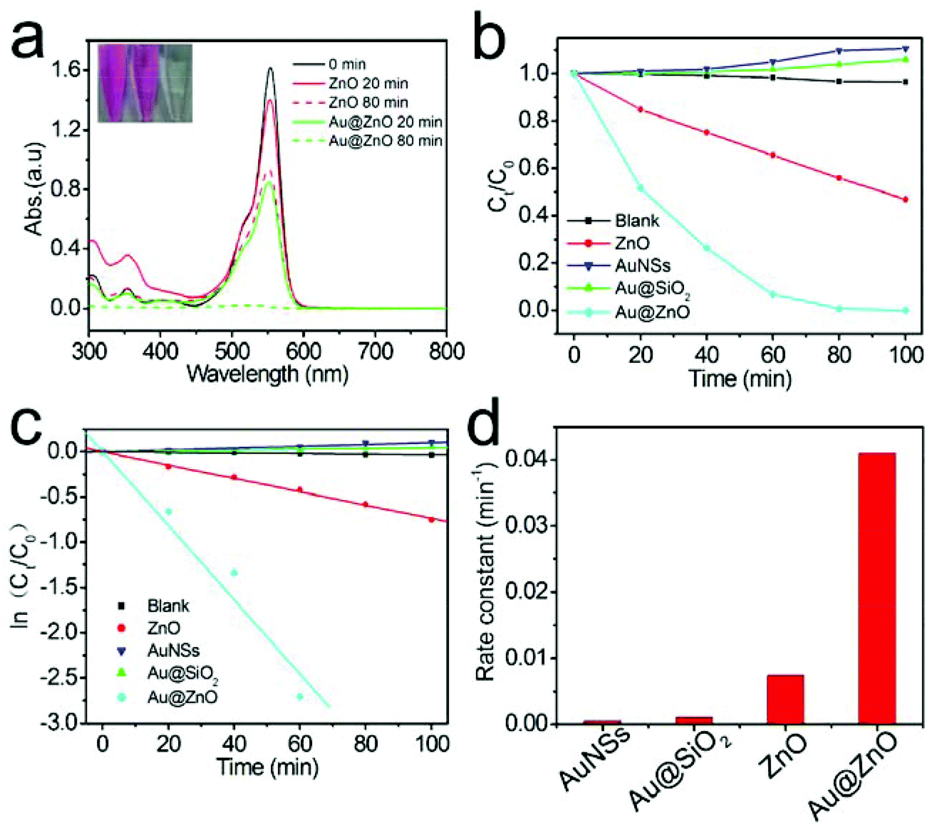 | ||
| Fig. 7 (a) Time-dependent UV-Vis absorption spectra of RhB aqueous solution in the presence of pure ZnO or Au@ZnO photocatalysts. The inset is a photograph of RhB solution sampled at 0 min, 20 min, and 80 min, respectively, using Au@ZnO as the photocatalyst. (b) RhB concentration evolution along the irradiation time over several different photocatalysts. (c) Kinetic linear fittings of photocatalytic reactions. (d) A histogram for the photodegradation reaction rate constants. | ||
To further reveal the specific contribution of the Au core and ZnO shell to the enhanced photocatalysis of Au@ZnO nanostructures, the photocatalytic degradation of RhB was carried out under the illumination of monochromatic LED light with three different wavelengths of 365 nm, 520 nm, and 660 nm, respectively. Fig. 8a shows the RhB concentration evolution under the LED light with three different wavelengths, using the Au@ZnO core–shell nanostructures as the photocatalyst. The kinetic fitting results of the photocatalytic degradation of RhB under LED light are shown in Fig. 8b, indicating that the photocatalytic RhB degradation under LED light also approximately follows the first-order reaction kinetics model. The photodegradation reaction rate constants k corresponding to LED light of 365 nm, 520 nm, and 660 nm were calculated to be 0.0326, 0.0118, and 0.0097 min−1, respectively, and are shown in the histogram in Fig. 8c. The above results indicate that the photocatalytic efficiency of Au@ZnO core–shell nanostructures is closely related to the irradiation wavelength. The Au@ZnO photocatalyst shows the highest photocatalytic activity under the LED light of 365 nm, which should be mainly contributed by the ZnO shells. However, the Au@ZnO photocatalyst also exhibits considerable photocatalytic activity under monochromatic visible light of 520 nm and 660 nm. The pure ZnO nanoparticles present little photocatalytic activity under the visible light because of its wide bandgap. As a result, the visible-light driven photocatalysis of the Au@ZnO nanostructures should stem from the plasmon sensitization effect of the Au-nanosphere cores.51,52 Moreover, it is understandable that the photocatalytic efficiency under 520 nm LED light is higher than that under the 660 nm LED light because of the strong light absorption at 520 nm of the Au@ZnO photocatalyst, as shown in Fig. 5. Therefore, the above results confirm that both the Au-nanosphere core and ZnO shell specifically contribute to the enhanced photocatalytic performance of the Au@ZnO core–shell nanostructures.
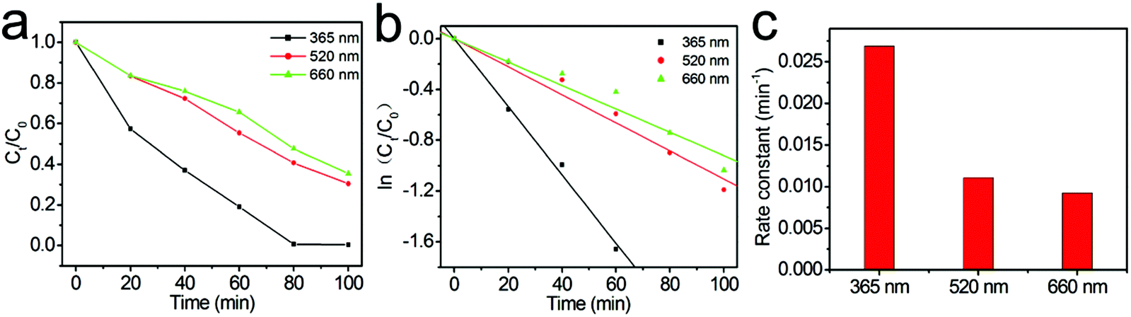 | ||
| Fig. 8 The photocatalytic degradation of RhB over Au@ZnO core–shell nanostructures under LED light with different wavelengths. (a) RhB concentration evolution along the irradiation time. (b) Kinetic linear fittings of photocatalytic reactions. (c) A histogram for the photocatalytic reaction rate constants. | ||
The photoresponse properties of the Au@ZnO photocatalyst have been tested as a photoelectrode material under switching the light source of the Xe lamp, by comparison with that of the pure ZnO nanoparticles. For preparing the working electrode, the photocatalyst was spin-coated on the ITO glass to form a film. The surface topography of both Au@ZnO and pure ZnO films on ITO glasses was analyzed from the AFM images (Fig. 9). The AFM images of the films present a granular morphology, which is mainly dominated by the densely packed grains. The average roughness values (Ra) of the Au@ZnO film (Fig. 9a and b) and pure ZnO film (Fig. 9c and d) were calculated to be 5.35 nm and 5.78 nm, respectively. The Ra value of the pure ZnO film is a little larger than that of the Au@ZnO film, may be due to more agglomeration of ZnO nanoparticles on the substrate. Fig. 10a shows the I–t curves of the Au@ZnO and pure ZnO film photoelectrodes tested under on–off cycle illumination conditions. Upon illumination, the Au@ZnO nanostructure film as a photoanode gives a higher photocurrent density of 0.06 mA cm−2 than that (0.05 mA cm−2) of the pure ZnO nanoparticle film, indicating the enhanced photoresponse of the Au@ZnO core–shell nanostructures. The enhancement should be due to the plasmonic harvesting of visible light by the Au-nanosphere cores in the Au@ZnO nanostructures. Besides, electrochemical impedance spectroscopy (EIS) has been commonly used to investigate the kinetics of charge transfer at the interface between the photoelectrode and electrolyte. Fig. 10b depicts the Nyquist plots of the Au@ZnO photoanode and the pure ZnO photoanode under Xe lamp irradiation. In the Nyquist plots, a semicircle at a high frequency represents the charge-transfer process, and the diameter of the semicircle reflects the charge-transfer resistance.53,54 Obviously, the semicircle diameter of the Au@ZnO photoanode is smaller than that of the pure ZnO photoanode, indicating that the Au nanospheres as cores can enhance the electron mobility by accelerating the separation of the photogenerated charges in the Au@ZnO core–shell nanostructures. The higher charge-transfer ability is thought to be another way for enhancing the photoelectrochemical performance. As a consequence, the improved photoelectrochemical performance further confirms the synergistic effect of the plasmonic Au-nanosphere core and the semiconducting ZnO shell which specifically contributes to the photocatalytic/photoelectrochemical properties.
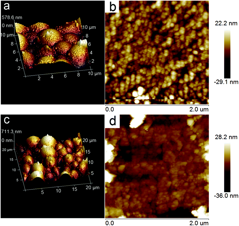 | ||
| Fig. 9 AFM images of (a, b) Au@ZnO core–shell nanostructure film and (c, d) ZnO nanoparticle film on ITO glass for photoelectrochemical tests. | ||
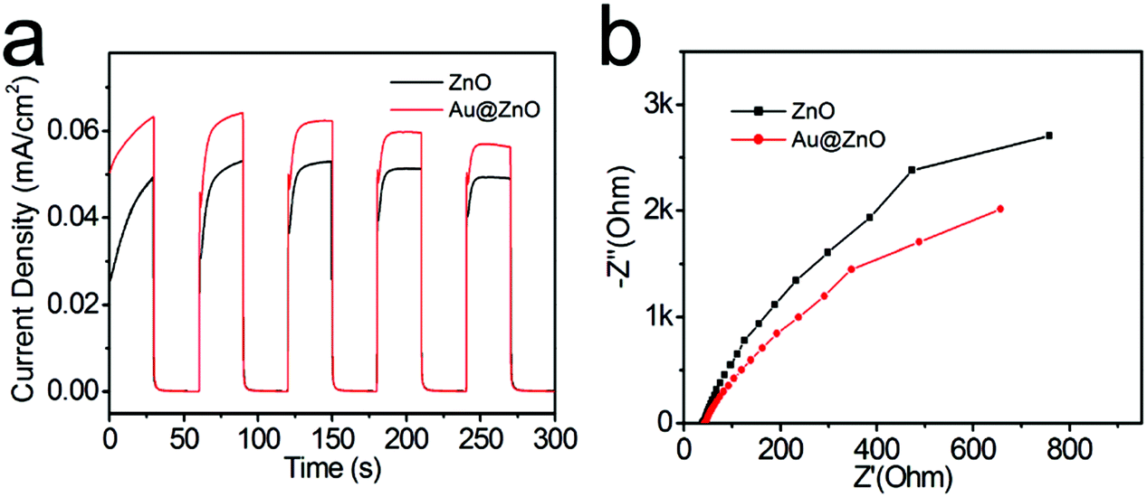 | ||
| Fig. 10 (a) I–t curves of the calcined Au@ZnO core–shell nanostructures and the calcined pure ZnO nanoparticles at an applied potential of 0.5 V vs. Ag/AgCl under the illumination of simulated sunlight during on/off cycles within 300 s, (b) Nyquist plots of the electrochemical impedance spectra of the two samples under simulated sunlight. | ||
Based on the above experimental results, reasonable explanations can be concluded as follows about the mechanism for the enhanced photocatalysis of the Au@ZnO core–shell nanostructures. Principally, the enhancement in the photocatalysis of the Au@ZnO nanostructures should be attributed to the synergistic effect between the plasmonic Au-nanosphere core and the semiconducting ZnO shell, as shown in Fig. 11. Under irradiation with simulated sunlight, the SPR of the Au-nanosphere core and the electron–hole pairs in the ZnO shell could be excited simultaneously. The photogenerated carriers were generated through the excitation of both the band-gap transition of the ZnO shell and the plasmon resonance of the Au-nanosphere core upon the irradiation. The Au-nanosphere cores extended the light-harvesting region of the photocatalyst due to their SPR properties, and greatly enhanced the photon utilization efficiency. Meanwhile, a plasmon-driven charge separation process may occur at the interface between the Au nanosphere and ZnO shell. The excited plasmon of Au-nanosphere cores in the core–shell nanostructures produced hot electrons, some of which have energies higher than the Schottky barrier at the interface and can cross the barrier, injecting into the conduction band of the semiconductor.23 The plasmonic energy transfer would remarkably enhance the concentration of photo-generated carriers in the photocatalyst, and therefore the photocatalytic/photoelectrochemical efficiencies were improved. In the case where only visible light was provided, the ZnO shell was hardly excited to give the photo-generated electron–hole pairs, and the photocatalysis resulted from a plasmonic sensitization process occurring at the interface between the plasmonic Au nanosphere and the ZnO shell.55 Besides, the special mesoporous structure and larger surface area of the ZnO shell could offer more opportunities for studying the diffusion and adsorption of substrate molecules and radicals during the photocatalytic reaction.
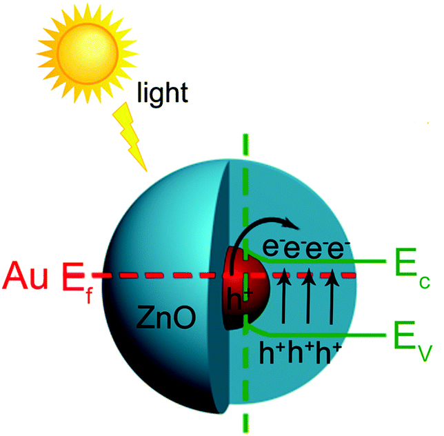 | ||
| Fig. 11 Schematic of the plasmonic enhancement mechanism for the Au@ZnO core–shell nanostructure photocatalyst under simulated sunlight. | ||
Conclusions
In summary, we prepared monodispersed Au@ZnO core–shell nanostructures with well-defined Au nanospheres as cores. After calcination at 350 °C in air, the mesoporous ZnO shell with higher crystallinity and a larger surface area formed without a significant change in the morphology or the SPR band of the Au@ZnO core–shell nanostructures. The structures and compositions of the core@shell nanostructures was confirmed by different characterization methods including XRD, SEM, TEM/HRTEM, STEM-mapping, SEM-mapping, UV−visible absorption spectrum and N2 adsorption–desorption isotherms. The Au@ZnO core–shell nanostructures showed a strong visible light absorption, due to the specific SPR properties of the Au-nanosphere cores. As expected, the Au@ZnO photocatalyst presented enhanced photocatalytic efficiency in the photodegradation of RhB under the illumination of both simulated sunlight and monochromatic LED visible light. Moreover, the Au@ZnO sample as a photoanode material gave a higher photocurrent density than that of the ZnO nanoparticles. The EIS Nyquist plots also confirmed the higher charge transfer efficiency of the Au@ZnO nanostructure photoelectrode. The improved photocatalytic and photoelectrochemical performances of the Au@ZnO nanostructures can be attributed to the synergistic effect of the plasmonic Au-nanosphere core and the semiconducting ZnO shell. The synergetic enhancement by plasmonic metal nanocrystals and semiconductors in metal–semiconductor hybrid nanostructures with specific structures and morphologies makes them suitable candidates for a wide range of applications. Therefore, such core–shell nanostructures would provide a desirable platform for studying plasmon-induced/enhanced processes and have great potential in light-harvesting applications.Acknowledgements
This work is supported by the National Natural Science Foundation of China (21471004), the China Postdoctoral Science Foundation of Special Funding (2015T80644), and the Excellent Youth Talents Support Plan in Colleges and Universities of Anhui Province.References
- M. R. Hoffmann, S. T. Martin, W. Choi and D. W. Bahnemann, Chem. Rev., 1995, 95, 69–96 CrossRef CAS.
- B. Ohtani, J. Photochem. Photobiol., C, 2010, 11, 157–178 CrossRef CAS.
- Y. Q. Qu and X. F. Duan, Chem. Soc. Rev., 2013, 42, 2568–2580 RSC.
- Y. Ma, X. L. Wang, Y. S. Jia, X. B. Chen, H. X. Han and C. Li, Chem. Rev., 2014, 114, 9987–10043 CrossRef CAS PubMed.
- B. Liu, X. Zhao, C. Terashima, A. Fujishima and K. Nakata, Phys. Chem. Chem. Phys., 2014, 16, 8751–8760 RSC.
- J. Schneider, M. Matsuoka, M. Takeuchi, J. Zhang, Y. Horiuchi, M. Anpo and D. W. Bahnemann, Chem. Rev., 2014, 114, 9919–9986 CrossRef CAS PubMed.
- U. Diebold, Nat. Chem., 2011, 3, 271–272 CrossRef CAS PubMed.
- K. Nakata and A. Fujishima, J. Photochem. Photobiol., C, 2012, 13, 169–189 CrossRef CAS.
- Y. Xu, Y. Huang and B. Zhang, Inorg. Chem. Front., 2016 10.1039/c5qi00217f.
- M. D. L. R. Peralta, U. Pal and R. S. Zeferino, ACS Appl. Mater. Interfaces, 2012, 4, 4807–4816 Search PubMed.
- F. J. Heiligtag, W. Cheng, V. R. Mendonça, M. J. Süess, K. Hametner, D. Günther, C. Ribeiro and M. Niederberger, Chem. Mater., 2014, 26, 5576–5584 CrossRef CAS.
- S. Linic, P. Christopher and D. B. Ingram, Nat. Mater., 2011, 10, 911–921 CrossRef CAS PubMed.
- F. Wang, C. H. Li, H. J. Chen, R. B. Jiang, L.-D. Sun, Q. Li, J. F. Wang, J. C. Yu and C.-H. Yan, J. Am. Chem. Soc., 2013, 135, 5588–5601 CrossRef CAS PubMed.
- S. Peiris, J. McMurtrie and H.-Y. Zhu, Catal. Sci. Technol., 2016, 6, 320–338 CAS.
- Z. Zhang, L. Zhang, M. N. Hedhili, H. Zhang and P. Wang, Nano Lett., 2013, 13, 14–20 CrossRef CAS PubMed.
- K. Bramhaiah, V. N. Singh and N. S. John, Phys. Chem. Chem. Phys., 2016, 18, 1478–1486 RSC.
- S. Sarina, H. Zhu, E. Jaatinen, Q. Xiao, H. Liu, J. Jia, C. Chen and J. Zhao, J. Am. Chem. Soc., 2013, 135, 5793–5801 CrossRef CAS PubMed.
- Y. Hartadi, D. Widmann and R. J. Behm, J. Catal., 2016, 333, 238–250 CrossRef CAS.
- J. Q. Jiao, Y. C. Wei, Z. Zhao, W. J. Zhong, J. Liu, J. M. Li, A. Duan and G. Y. Jiang, Catal. Today, 2015, 258, 319–326 CrossRef CAS.
- Y. Z. Chen, D. Q. Zeng, K. Zhang, A. Lu, L. S. Wang and D.-L. Peng, Nanoscale, 2014, 6, 874–881 RSC.
- S. T. Kochuveedu, Y. H. Jang and D. H. Kim, Chem. Soc. Rev., 2013, 42, 8467–8493 RSC.
- S. K. Dutta, S. K. Mehetor and N. Pradhan, J. Phys. Chem. Lett., 2015, 6, 936–944 CrossRef CAS PubMed.
- R. B. Jiang, B. X. Li, C. H. Fang and J. F. Wang, Adv. Mater., 2014, 26, 5274–5309 CrossRef CAS PubMed.
- P. Sudhagar, A. Devadoss, T. Song, P. Lakshmipathiraj, H. Han, V. V. Lysak, C. Terashima, K. Nakata, A. Fujishima, U. Paik and Y. S. Kang, Phys. Chem. Chem. Phys., 2014, 16, 17748–17755 RSC.
- Y. Z. Chen, D. Q. Zeng, M. B. Cortie, A. Dowd, H. Z. Guo, J. B. Wang and D. L. Peng, Small, 2015, 11, 1460–1469 CrossRef CAS PubMed.
- B. X. Li, Y. G. Hao, X. K. Shao, H. D. Tang, T. Wang, J. B. Zhu and S. L. Yan, J. Catal., 2015, 329, 368–378 CrossRef CAS.
- S. Han, L. F. Hu, N. Gao, A. A. Al-Ghamdi and X. Fang, Adv. Funct. Mater., 2014, 24, 3725–3733 CrossRef CAS.
- T.-H. Yang, L.-D. Huang, Y.-W. Harn, C.-C. Lin, J.-K. Chang, C.-I. Wu and J.-M. Wu, Small, 2013, 9(18), 3169–3182 CrossRef CAS PubMed.
- W. He, H.-K. Kim, W. G. Wamer, D. Melka, J. H. Callahan and J.-J. Yin, J. Am. Chem. Soc., 2014, 136, 750–757 CrossRef CAS PubMed.
- C. G. Silva, M. J. Sampaio, S. A. C. Carabineiro, J. W. L. Oliveira, D. L. Baptista, R. Bacsa, B. F. Machado, P. Serp, J. L. Figueiredo, A. M. T. Silva and J. L. Faria, J. Catal., 2014, 316, 182–190 CrossRef CAS.
- D. Zheng, X. Pang, M. Wang, Y. He, C. Lin and Z. Lin, Chem. Mater., 2015, 27, 5271–5278 CrossRef CAS.
- C.-H. Kuo, Y.-C. Yang, S. Gwo and M. H. Huang, J. Am. Chem. Soc., 2011, 133, 1052–1057 CrossRef CAS PubMed.
- L. Kong, W. Chen, D. Ma, Y. Yang, S. Liu and S. Huang, J. Mater. Chem., 2012, 22, 719–724 RSC.
- M. Misra, P. Kapur and M. L. Singla, Appl. Catal., B, 2014, 150, 605–611 CrossRef.
- C. H. Fang, H. L. Jia, S. Chang, Q. F. Ruan, P. Wang, T. Chen and J. F. Wang, Energy Environ. Sci., 2014, 7, 3431–3438 CAS.
- P. Peerakiatkhajohn, T. Butburee, J.-H. Yun, H. Chen, R. M. Richards and L. Wang, J. Mater. Chem. A, 2015, 3, 20127–20133 CAS.
- J. Goebl, J. B. Joo, M. Dahl and Y. Yin, Catal. Today, 2014, 225, 90–95 CrossRef CAS.
- S. K. Cushing, J. Li, J. Bright, B. T. Yost, P. Zheng, A. D. Bristow and N. Wu, J. Phys. Chem. C, 2015, 119, 16239–16244 CAS.
- N. Udawatte, M. Lee, J. Kim and D. Lee, ACS Appl. Mater. Interfaces, 2011, 3, 4531–4538 CAS.
- Z. Xu, C. Zhang, W. Wang, Y. Bando, X. Baib and D. Golberg, Nano Energy, 2015, 13, 233–239 CrossRef CAS.
- J. Xu, Z. a. Chen, J. A. Zapien, C.-S. Lee and W. Zhang, Adv. Mater., 2014, 26, 5337–5367 CrossRef CAS PubMed.
- S. M. Majhi, P. Rai and Y.-T. Yu, ACS Appl. Mater. Interfaces, 2015, 7, 9462–9468 CAS.
- K. Keis, C. Bauer, G. Boschloo, A. Hagfeldt, K. Westermark, H. Rensmo and H. Siegbahn, J. Photochem. Photobiol., A, 2002, 148, 57–64 CrossRef CAS.
- S. Maiti, S. Pal and K. K. Chattopadhyay, CrystEngComm, 2015, 17, 9264–9295 RSC.
- Q. Ruan, L. Shao, Y. Shu, J. F. Wang and H. K. Wu, Adv. Opt. Mater., 2014, 2, 65–73 CrossRef.
- I. Gorelikov and N. Matsuura, Nano Lett., 2008, 8, 369–373 CrossRef CAS PubMed.
- Y. Yang, S. Han, G. Zhou, L. Zhang, X. Li, C. Zou and S. Huang, Nanoscale, 2013, 5, 11808–11819 RSC.
- H. J. Chen, L. Shao, Q. Li and J. F. Wang, Chem. Soc. Rev., 2013, 42, 2679–2724 RSC.
- B. X. Li, T. Gu, T. Ming, J. X. Wang, P. Wang, J. F. Wang and J. C. Yu, ACS Nano, 2014, 8, 8152–8162 CrossRef CAS PubMed.
- H. J. Chen, X. S. Kou, Z. Yang, W. H. Ni and J. F. Wang, Langmuir, 2008, 24, 5233–5237 CrossRef CAS PubMed.
- C. L. Wang and D. Astruc, Chem. Soc. Rev., 2014, 43, 7188–7216 RSC.
- F.-X. Xiao, Z. P. Zeng and B. Liu, J. Am. Chem. Soc., 2015, 137, 10735–10744 CAS.
- M. Wu, W.-J. Chen, Y.-H. Shen, F.-Z. Huang, C.-H. Li and S.-K. Li, ACS Appl. Mater. Interfaces, 2014, 6, 15052–15060 CAS.
- T. Wang, R. Lv, P. Zhang, C. L. Li and J. L. Gong, Nanoscale, 2015, 7, 77–81 RSC.
- L. Q. Liu, S. X. Ouyang and J. H. Ye, Angew. Chem., Int. Ed., 2013, 52, 6689–6693 CrossRef CAS PubMed.
Footnote |
| † Electronic supplementary information (ESI) available. See DOI: 10.1039/c6qi00064a |
| This journal is © the Partner Organisations 2016 |