
Reduction of thermal conductivity through nanostructuring enhances the thermoelectric figure of merit in Ge1−xBixTe†
Suresh
Perumal‡
,
Subhajit
Roychowdhury‡
and
Kanishka
Biswas
*
New Chemistry Unit, Jawaharlal Nehru Centre for Advanced Scientific Research (JNCASR), Jakkur P.O., Bangalore 560064, India. E-mail: kanishka@jncasr.ac.in
First published on 18th November 2015
Abstract
A promising thermoelectric figure of merit, zT, of ∼1.3 at 725 K was obtained in high quality crystalline ingots of Ge1−xBixTe. The substitution of Bi3+ in a Ge2+ sublattice of GeTe significantly reduces the excess hole concentration due to the aliovalent donor dopant nature of Bi3+. Reduction in carrier density optimizes electrical conductivity, and subsequently enhances the Seebeck coefficient in Ge1−xBixTe. More importantly, a low lattice thermal conductivity of ∼1.1 W m−1 K−1 for Ge0.90Bi0.10Te was achieved, which is due to the collective phonon scattering from meso-structured grain boundaries, nano-structured precipitates, nano-scale defect layers, and solid solution point defects. We have obtained a reasonably high mechanical stability for the Ge1−xBixTe samples. The measured Vickers microhardness value of the high performance sample is ∼165 HV, which is comparatively higher than that of state-of-the-art thermoelectric materials, such as PbTe, Bi2Te3, and Cu2Se.
 Kanishka Biswas | Kanishka Biswas obtained his MS and Ph.D degree from the Solid State Structural Chemistry Unit, Indian Institute of Science (2009) and did postdoctoral research at the Department of Chemistry, Northwestern University (2009–2012). He is an Assistant Professor in the New Chemistry Unit, Jawaharlal Nehru Centre for Advanced Scientific Research (JNCASR), Bangalore. He is pursuing research in solid state inorganic chemistry of metal chalcogenides, thermoelectrics, topological insulators and the intergrowth of 2D nanosheets. He has published 69 research papers and 3 book chapters. He is a co-author of a book entitled “Essentials of inorganic materials synthesis” published by John Wiley and Sons, Inc in 2015. He is a recipient of the Ramanujan Fellowship from the Department of Science and Technology, India. He is a Young Affiliate of The World Academy of Sciences (TWAS) and an Associate of the Indian Academy of Science, India. He is also a recipient of the Young Scientist Platinum Jubilee award-2015 from The National Academy of Sciences (NASI), India. |
Introduction
Thermoelectric (TE) materials have the potential to play a predominant role in future energy management by converting fractions of waste heat into useful electricity.1–4 The conversion efficiency of TE materials is determined by the material's thermoelectric figure of merit, zT = S2σT/κtotal, where, S, σ, κtotal and T are the Seebeck coefficient, electrical conductivity, total thermal conductivity and temperature, respectively. The decoupling of these interdependent parameters, S, σ, and κtotal, is a great challenge in enhancing the zT. Nevertheless, significant attempts have been made to increase zT by enhancing the power factor, S2σ, via minority carrier energy filtering,5a the formation of resonance energy levels and degenerate states close to the Fermi level (EF),5b,c valence and conduction band convergence,5d–g and the quantum confinement effect.5f In addition, substantial efforts have been taken to reduce lattice thermal conductivity by increasing phonon scattering via introducing solid solution point defects, embedding endotaxial nano-inclusions as second phases in the matrix,6,7a and forming the meso-scale grain boundaries7 and due to intrinsic bond anharmonicity.8IV–VI metal chalcogenides, PbTe, SnTe and GeTe, are regarded as the present state-of-the-art high performance thermoelectric materials that are capable of working in an intermediate temperature range of 600–900 K.1,3,5–7 Amongst these, well-known PbTe based materials have been extensively studied from a materials' aspect to a device level; however, the toxic nature of Pb limits its use in terms of large scale thermoelectric applications.
GeTe has been regarded as one of the known promising p-type narrow band gap thermoelectric materials since the 1960s;9 but it has not attracted much attention due to its large p-type carrier density (∼1021 cm−3) that comes from its intrinsic Ge vacancy.10 High carrier concentration in GeTe results in a high electrical conductivity of ∼8500 S cm−1, low Seebeck coefficient value of ∼30 μV K−1, and a perversely high total thermal conductivity of ∼8 W m−1 K−1 at 300 K, thus leading to a maximum zT value of 0.7 at 720 K.11 Undoped GeTe undergoes the ferroelectric structural phase transition from a high temperature cubic structure (β-phase) to a low temperature rhombohedral structure (α-phase) at ∼700 K due to the thermal strain induced shift in the Ge atoms (Fig. 1a), which thrusts the distortion in the unit cell along the [111] direction with an angular distortion of α = 1.65°.12
 | ||
| Fig. 1 (a) Photograph of the high quality ingot, sliced bar and pellet, Crystal structure of GeTe, which is rhombohedral at 300 K and cubic at 673 K; (b) powder XRD patterns of the Ge1−xBixTe samples; (c) zoomed XRD pattern of (b) in between the angles (2θ) of 40° to 45°, that shows the merging of the (024) and (220) peaks with increasing Bi doping; and (d) optical absorption spectra of the Ge1−xBixTe samples. | ||
GeTe-rich compositions with AgSbTe2, recognized as TAGS-80 [(GeTe)0.80(AgSbTe2)0.20] and TAGS-85 [(GeTe)0.85(AgSbTe2)0.15], are being considered as traditional thermoelectric materials with a reasonably high zT of 1.3.13 Recently, GexPb1−xTe has been reported to be a high performance thermoelectric material due to the donor dopant nature of Pb which significantly increases the Seebeck coefficient by reducing the carrier density, and furnishes a low thermal conductivity generated from the various thermodynamically driven nanoscale modulations.14 A zT of ∼1.9 at 773 K was obtained in 3 mol% Bi2Te3 doped Ge0.87Pb0.13Te samples due to the thermal conductivity reduction from point defect scattering of phonons and enhancement of the power factor through valence band convergence.15 3 mol% Bi2Te3 doping in Ge0.87Pb0.13Te promoted the solubility of PbTe in GeTe and enhanced the valence band convergence. Composition variation and thermal treatment in Ge–Sb–Te based alloys resulted in parquet-like nanoscale defect layers and meso-structured domain variants, and twin and inversion boundaries, which significantly reduced the lattice thermal conductivity, and thus led to maximum zT values of ∼1.9.16 Moreover, a recent report on Sb doping in GeTe resulted in a significantly high zT of ∼1.85 and high mechanical stability compared to that of other thermoelectric materials.16a Motivated by the low thermal conductivity, high zT and enhanced mechanical stability of Sb doped GeTe, herein an attempt has been made to understand the effect of Bi doping on the thermoelectric performance and mechanical stability of GeTe.
Here, we report the promising thermoelectric performance and reasonably high mechanical stability of Ge1−xBixTe (x = 0–0.10) samples. The substitution of Bi in GeTe decreases the hole concentration due to its donor dopant nature, which optimizes the Seebeck coefficient and electronic transport properties. We have achieved a low lattice thermal conductivity of ∼1.1 W m−1 K−1 for Ge0.90Bi0.10Te, which is reasonably low compared with those of other high performance GeTe based materials. Significant thermal conductivity reduction was achieved due to collective phonon scattering from meso-structured grain boundaries, nano-structured precipitates, nano-structured defect layers, and solid solution point defects. The maximum figure of merit, zT, of ∼1.3 was achieved for the composition of Ge0.94Bi0.06Te at 725 K. Additionally, a Vickers microhardness value of ∼165 HV was measured for the Ge0.94Bi0.06Te sample, which is significantly higher than that of pristine GeTe (∼145 HV) and other state-of-the-art thermoelectric materials, such as PbTe, SnTe and Bi2Te3 based materials.
Experimental section
Reagents
Germanium (99.995%), bismuth (99.9999%) and tellurium (99.999%) were used for the synthesis without further purification.Synthesis
High quality crystalline ingots (∼6 g) of Ge1−xBixTe (x = 0–0.10) were prepared using a vacuum sealed quartz tube (10−6 Torr) melting reaction of a stoichiometric amount of the starting elements of Ge, Bi and Te. Typically, to synthesize the Ge0.94Bi0.06Te sample, Ge (1.9692 g, 27.109 mmol), Bi (0.3625 g, 1.735 mmol), and Te (3.6749 g, 28.800 mmol) were added into a quartz tube of 10 mm diameter. The tube was sealed under vacuum (10−6 Torr) and slowly heated to 1223 K over 10 h, then soaked for 6 h, and then slowly cooled down to room temperature over 10 h. The density of all the samples was measured using Archimedes’ method, which was ∼99% of the theoretical density (∼6.18 g cc−1). In order to measure the thermoelectric properties, ingots were sliced into pellets and bars by using a low speed diamond saw (Fig. 1a).Powder X-ray diffraction
Powder X-ray diffraction patterns were recorded for finely ground samples using Cu-Kα (λ = 1.5406 Å) radiation on a Bruker D8 diffractometer.Band gap measurement
To estimate the optical band gap of the as-synthesized samples, diffuse reflectance measurements were done with the finely ground powder sample at room temperature using a FT-IR Bruker IFS 66 V/S spectrometer in the wave number range of 4000–400 cm−1 with 2 cm−1 resolution and 50 scans. Absorption (α/Λ) data were calculated from reflectance data using the Kubelka–Munk equation: α/Λ = (1 − R)2/(2R), where R is the reflectance, and α and Λ are the absorption and scattering coefficient, respectively. The energy band gaps were derived from an α/Λ vs. Eg (eV) plot.Transmission electron microscopy
An aberration corrected FEI TITAN 3™ 80–300 KV transmission electron microscope was used to investigate the nanostructure in the Ge1−xBixTe samples. The samples were prepared by mechanical polishing followed by ion beam polishing/milling to achieve thin foils of ∼20–80 nm. Bright field imaging, high resolution TEM imaging and selected area electron diffraction (SAED) were carried out using a TEM.Electrical transport
Electrical conductivity and Seebeck coefficients were measured simultaneously under a He atmosphere from room temperature to 773 K on a ULVAC-RIKO ZEM-3 instrument system. A typical sample for measurement had a parallelepiped shape with the dimensions of ∼2 × 2 × 8 mm3. The longer direction coincides with the direction in which the thermal conductivity was measured. The heating and cooling cycles of the transport data confirmed the thermal stability (Fig. S1, ESI†).Hall measurement
The Hall measurement was carried out at room temperature in a home made setup, where a fixed magnetic field and dc-current of 0.25 T and 5 mA were used, respectively. The carrier concentration (n) was calculated from the equation: n = 1/(eRH), where RH is the Hall coefficient and e is the electron charge.Thermal conductivity
The thermal diffusivity, D, was directly measured in the range of 300–773 K by using the laser flash diffusivity method in a Netzsch LFA-457 (Fig. S2, ESI†). Coins with ∼8 mm diameter and ∼2 mm thickness were used in all of the measurements. The temperature dependent heat capacity, Cp, was derived using a standard sample (pyroceram) in a LFA-457, which is in good agreement with the Dulong–Petit Cp value (Fig. S3, ESI†). The total thermal conductivity, κtotal, was calculated using the formula: κtotal = DCpρ, where ρ is the density. The measured densities of all the samples were about 99% of the theoretical density (6.18 g cc−1)Mechanical properties
The microhardness of all the samples was measured on the Vickers hardness scale using a diamond indenter by means of a commercial Zwick Roell ZHU 2.5 instrument. The applied force and holding time were kept as 2 N and 10 s, respectively. The Vickers hardness values (kgf mm−2) were determined from the equation HV = 1. 854 × L/(2d)2, where L is the indentation load and 2d is the diagonal length of the indentation. The Vickers microhardness impressions of the indenter after unloading are shown in Fig. S4 (see ESI†). The uncertainty of the microhardness measurement is about 5%.Results and discussion
Crystalline ingots of Ge1−xBixTe (x = 0.00, 0.02, 0.06 and 0.10) were synthesized using a vacuum sealed tube melting reaction and the structural properties were analysed using powder X-ray diffraction (PXRD). Fig. 1b presents the PXRD patterns of Ge1−xBixTe, the peaks could be indexed based on a rhombohedral GeTe (R3m) structure. Typically, the presence of double peaks in the range of 2θ = 23° to 27° and 2θ = 41° to 45° further confirms the rhombohedral phase. Additionally, the substitution of Bi in GeTe tends to merge these double peaks into a single peak (see Fig. 1c). During this substitution, Bi tries to rearrange the positions of Ge from (½ − x ½ − x ½ − x) to (½ ½ ½), which indicates that the cubic nature of the system increases with Bi doping in GeTe. A similar result was observed previously in the case of Sb doped GeTe.16aThe spectroscopically measured band gaps of the Ge1−xBixTe samples are shown in Fig. 1d. The optical band gap of pure GeTe is observed to be ∼0.21 eV. The substitution of Bi in GeTe substantially reduces the band gap from ∼0.21 eV to 0.08 eV (Fig. 1d). In GeTe, Te (electronegativity∼2.10 in the Pauling scale) forms a valence band, whereas Ge (electronegativity ∼2.01) contributes to the conduction band. The reduction in the band gap is due to the formation of Bi states below the conduction band because of its donor dopant nature and the slightly higher electronegativity of Bi (∼2.02) compared to that of Ge. Previously reported first principle electronic structure calculations also indicate the decrease in the band gap of GeTe after Bi doping due to the lowering of the conduction band energy.17
Nano/microstructures of Ge0.90Bi0.10Te were investigated using aberration corrected TEM and the results are shown in Fig. 2. The low magnification TEM micrograph of Ge0.9Bi0.1Te is presented in Fig. 2a, which clearly shows the presence of nanoprecipitates with a dark contrast in the matrix of GeTe. In Fig. 2b, the high magnification micrograph illustrates ∼100–200 nm sized fine grains of GeTe (marked in yellow dotted circles). The nanoprecipitates with sizes in the range of 5–20 nm are observed in the high resolution TEM micrograph in Fig. 2c. Although it was really difficult to determine the actual composition of the nanoprecipitates using energy dispersive X-ray spectroscopy, we speculate that the nanoprecipitates are indeed Bi rich phases which are embedded in the GeTe matrix. The presence of nanoscale parallel cation-position like defect layers in the van der Waals gaps are also clearly seen throughout the samples (see Fig. 2d). These defect layers are formed because of strongly disordered octahedral voids between the successive Te–Te layers. Moreover, the inset of Fig. 2d shows the diffused selected area electron diffraction (SAED) pattern, which is obtained from the defect layer region. Additionally, these defects seemed to be thermodynamically less stable as they disappear upon prolonged exposure to a high energy electron beam, even for 1 min exposure. Fig. 2e illustrates the HRTEM micrographs of the defect-free region, a zoomed area from Fig. 2d, with the corresponding SAED pattern with clear spots (inset of Fig. 2e). The HRTEM micrograph of the defect-free region illustrates an interplanar spacing of ∼0.34 nm that corresponds to (021) lattice planes of GeTe, (see Fig. 2f), which further confirms the rhombohedral R3m phase. Defect-free regions show clearly separated diffraction spots (see inset Fig. 2f).
 | ||
| Fig. 2 (a) Low magnification TEM micrograph of Ge0.90Bi0.10Te with Bi-rich nano-precipitates, (b) TEM image shows mesoscale grain boundaries (dotted yellow circles), (c) HRTEM images shows nanoprecipitates, (d) parallel defect layers and their corresponding SAED pattern with diffusive spots, (e) HRTEM micrographs in the defect free region with clear SAED spots and (f) HRTEM micrograph of Ge0.90Bi0.10Te shows an inter planar spacing of 0.34 nm (inset shows the corresponding SAED pattern). | ||
Fig. 3a presents the electrical conductivity, σ, of the Ge1−xBixTe (x = 0–0.10) samples as a function of temperature. The σ of all the samples decreases with increasing temperature, which is typically observed for degenerate semiconductors. Pristine GeTe exhibits the σ value of ∼8067 S cm−1 at 300 K, which decreases to ∼2158 S cm−1 at 708 K. Around 673 K, σ vs. T data shows an anomaly which is due to a structural transition (R3m to Fm![[3 with combining macron]](https://www.rsc.org/images/entities/char_0033_0304.gif) m) in GeTe. Furthermore, the addition of Bi of 10 mol% in GeTe drastically reduces the σ value from ∼8067 S cm−1 to ∼986 S cm−1, due to the reduction in the carrier concentration. A Hall measurement was performed to measure the room temperature hole concentration. Typically, the calculated carrier density, n, is ∼8.7 × 1020 cm−3 for GeTe which decreases to ∼1.24 × 1020 cm−3 for Ge0.94Bi0.06Te. This reduction in p-type carrier concentration is attributed to the aliovalent dopant nature of Bi3+ at the Ge2+ site in GeTe which gives rise to the extra electron in the system.
m) in GeTe. Furthermore, the addition of Bi of 10 mol% in GeTe drastically reduces the σ value from ∼8067 S cm−1 to ∼986 S cm−1, due to the reduction in the carrier concentration. A Hall measurement was performed to measure the room temperature hole concentration. Typically, the calculated carrier density, n, is ∼8.7 × 1020 cm−3 for GeTe which decreases to ∼1.24 × 1020 cm−3 for Ge0.94Bi0.06Te. This reduction in p-type carrier concentration is attributed to the aliovalent dopant nature of Bi3+ at the Ge2+ site in GeTe which gives rise to the extra electron in the system.
 | ||
| Fig. 3 Temperature dependent (a) electrical conductivity (σ) and (b) Seebeck coefficient (S) of the Ge1−xBixTe samples. (c) Pisarenko plots (S vs. n data) for the Ge1−xBixTe samples which are compared with earlier reported data. (d) Temperature dependent power factor (S2σ) of the Ge1−xBixTe samples. | ||
Fig. 3b presents the Seebeck coefficient value, S, of the Ge1−xBixTe (x = 0–0.10) samples as a function of temperature. For all the samples, a positive sign of S indicates that the holes are responsible for thermoelectric transport, which supports the Hall coefficient data. At 300 K, GeTe has an S value of ∼34 μV K−1 which increases with temperature, then reaches ∼153 μV K−1 at 708 K.11a It is expected that the doping of Bi in GeTe would increase the S value as it drastically reduces the hole concentration. Typically, 10 mol% of Bi doping in GeTe increases the S value to ∼98 μV K−1 at 300 K, which reaches a maximum value of ∼236 μV K−1 at 708 K. The increase of the Seebeck coefficient by Bi substitution is mainly due to the decrease in hole concentration, which will be clear from the Pisarenko plot (next section).
Fig. 3c shows the measured Seebeck values, S, as a function of hole density, n, for GeTe and Ge0.94Bi0.06Te, which are compared with the Pisarenko plots at different temperatures of 323 K and 623 K.14a,d,15,16 We have also compared the present S vs. n data with previously reported other high performance GeTe based materials such as, Ge1−xSbxTe,16a (GeTe)1−x[(PbTe)(SnTe)(Bi2Te3)]x,14a Ge1−xPbxTe,14d and 3 mol% Bi2Te3 doped Ge0.87Pb0.13Te.15 The S vs. n data of Ge1−xBixTe follows the Pisarenko relation, which indicates that the enhancement in the Seebeck coefficient upon Bi doping in GeTe is mainly due to the decrease in carrier concentration.
Fig. 3d illustrates the power factor, S2σ, of the Ge1−xBixTe (x = 0–0.10) samples as a function of temperature. Typically, the Ge0.94Bi0.06Te samples show an S2σ value of ∼12 μW cm−1 K−2 at 300 K, which reaches a maximum of ∼40 μW cm−1 K−2 at 712 K. Although the S values increase upon Bi doping in GeTe, it does not improve the S2σ values due to a large reduction in electrical conductivity.
Fig. 4a presents the total thermal conductivity, κtotal, of the Ge1−xBixTe (x = 0–0.10) samples as a function of temperature. Typically, pristine GeTe has a κtotal value of ∼8.3 W m−1 K−1 at 300 K, which decreases to ∼3.4 W m−1 K−1 at 673 K. It must be mentioned that the increase in the κtotal above 673 K in undoped GeTe is due to the rhombohedral to cubic structural phase transition. This trend was earlier observed for other GeTe based materials.16a With increasing Bi concentration, the κtotal drastically reduces from ∼8.3 W m−1 K−1 for GeTe to ∼1.6 W m−1 K−1 for Ge0.90Bi0.10Te at 300 K.
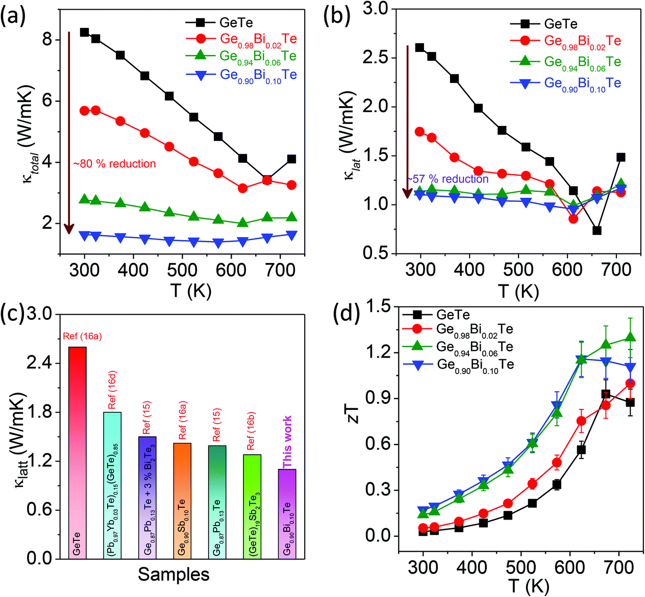 | ||
| Fig. 4 Temperature dependent (a) total thermal conductivity, κtotal, and (b) lattice thermal conductivity, κlatt, of the Ge1−xBixTe samples. (c) Comparison of the κlatt of the present Ge0.90Bi0.10Te sample with the previously reported high performance GeTe based materials. (d) Dimensionless thermoelectric figure of merit, zT, of the Ge1−xBixTe samples. | ||
The electronic thermal conductivity, κe, as a function of temperature for Ge1−xBixTe (x = 0–0.10) is presented in Fig. S5 (see ESI†). κe was calculated via the Wiedemann–Franz law, κe = σLT, where L is the Lorenz number. L, can be obtained based on the fitting of the respective Seebeck values that estimate the reduced chemical potential assuming a single parabolic band model as per eqn (1) (Fig. S6, ESI†).8c,18
 | (1) |
Pristine GeTe has the κe value of ∼5.6 W m−1 K−1 at 300 K, which suggests that carriers are mainly responsible for heat transport in GeTe. Due to the donor dopant nature of Bi in GeTe, it reduces the p-type carrier density and significantly decreases κe. Typically, 10 mol% of Bi in GeTe reduces the κe value from 5.66 W m−1 K−1 to 0.58 W m−1 K−1, which is about a 90% reduction as compared to that of undoped GeTe.
The κlat value of all the samples was obtained by subtracting κe from κtotal (Fig. 4b). The κlat value of Ge1−xBixTe decreases with the increase in Bi concentration. At 300 K, the κlat of GeTe is ∼2.6 W m−1 K−1, which is reduced to ∼1.1 W m−1 K−1 for Ge0.90Bi0.10Te; this is a ∼57% reduction in κlat. We have compared the κlat of the present Ge0.90Bi0.10Te sample with those of previously reported high performance GeTe based materials (see Fig. 4c). The Ge0.90Bi0.10Te sample exhibits one of the lowest values of κlat among the reported GeTe based materials. The low κlat in Ge1−xBixTe is attributed to the increased phonon scattering of meso-scale grain boundaries, nano-scale Bi rich precipitates, defect layers and atomic-scale point defects due to mass fluctuations.
Fig. 4d illustrates the thermoelectric figure of merit, zT, of the Ge1−xBixTe (x = 0.00, 0.02, 0.06 & 0.10) samples as a function of temperature. A maximum zT of ∼1.3 is achieved for the composition of Ge0.94Bi0.06Te at 725 K. The error in the overall zT estimation is ∼10% which includes the errors from electrical conductivity, and the Seebeck and thermal conductivity measurement. The high zT samples were re-measured and subjected to a cycling measurement (heating and cooling cycle), which shows good reproducibility that indicates that the prepared samples are thermally stable during thermal treatments/cycles (see Fig. S1, ESI†).
Besides a high zT, materials should be mechanically stable during machining in order to be used in large scale device application. We have measured mechanical properties using the Vickers microhardness indentation method (see Fig. 5). Generally, undoped GeTe material contains excess Ge vacancies which reduces the mechanical strength of GeTe. Bi doping reduces these Ge vacancies, and increases the rigidity of the material. Thus, Bi doping in GeTe helps to improve the mechanical properties. The Ge0.94Bi0.06Te sample shows the measured microhardness value of ∼165 HV, which is considerably higher than that of the state-of-the-art thermoelectric materials such as Bi2Te3,19a PbTe,19b,c,20a Pb–Sn–Te,20b PbSe,20c Cu2S![[thin space (1/6-em)]](https://www.rsc.org/images/entities/char_2009.gif) 20d and Cu2Se,20d and is relatively comparable to that of other GeTe based materials.21
20d and Cu2Se,20d and is relatively comparable to that of other GeTe based materials.21
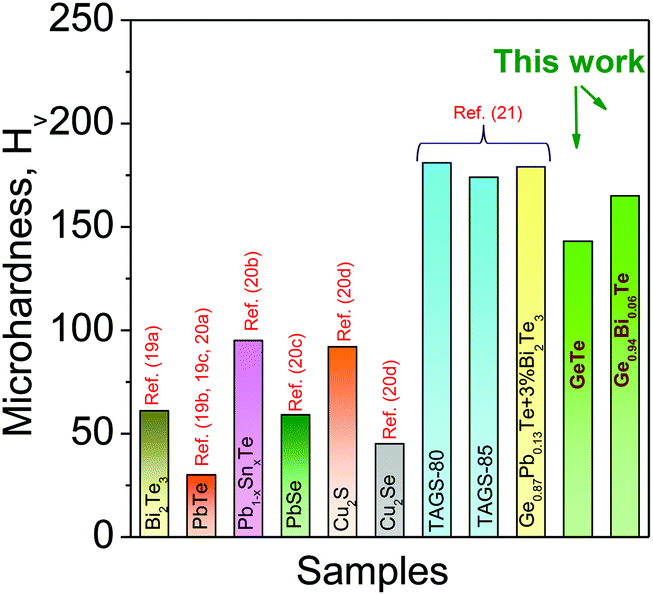 | ||
| Fig. 5 Vickers microhardness values, HV, of Ge0.94Bi0.06Te which are compared with selected popular thermoelectric materials. | ||
Conclusion
We have synthesized high quality ingots of Ge1−xBixTe (x = 0–0.10) using a vacuum sealed-tube melting reaction. Bi doping reduces the excess hole density in GeTe due to its aliovalent donor dopant nature. The obtained reduction in carrier density decreases the electrical conductivity and adversely increases the Seebeck coefficient in Ge1−xBixTe. Moreover, a low lattice thermal conductivity of ∼1.1 W mK−1 was achieved in Ge0.90Bi0.10Te, which is due to collective phonon scattering from meso-structured grain boundaries, nano-structured precipitates, nano-structured defect layers, and solid solution point defects. Overall, a maximum zT value of ∼1.3 was obtained for the composition of Ge0.94Bi0.06Te at 725 K, which is ∼35% higher than that of pristine GeTe. The measured Vickers micro-hardness value of Ge0.94Bi0.06Te is 165 HV, which is considerably higher than that of present state-of-the-art thermoelectric materials, such as PbTe and Bi2Te3.Acknowledgements
We thank Prof. C. N. R. Rao for the constant support. This work was partially supported by the DRDO-JNCASR collaborative project and DAE-BRNS project (37(3)20/01/2015/BRNS). K. B. acknowledges the partial support of the DST Ramanujan Fellowship and Sheikh Saqr Laboratory. We acknowledge Devendra S. Negi for TEM sample preparation and microscopy investigation. S. R. acknowledges CSIR for the PhD fellowship.Notes and references
- G. J. Snyder and E. S. Toberer, Nat. Mater., 2008, 7, 105 CrossRef CAS PubMed.
- L. D. Zhao, V. P. Dravid and M. G. Kanatzidis, Energy Environ. Sci., 2014, 7, 25 Search PubMed.
- J. Sootsman, D. Y. Chung and M. G. Kanatzidis, Angew. Chem., Int. Ed., 2009, 48, 8616 CrossRef CAS PubMed.
- (a) M. Zebarjadi, K. Esfarjani, M. S. Dresselhaus, Z. F. Ren and G. Chen, Energy Environ. Sci., 2012, 5, 5147 RSC; (b) T. Zhu, C. Fu, H. Xie, Y. Liu and X. Zhao, Adv. Energy Mater., 2015, 5 Search PubMed , 1500588; (c) K. Nielsch, J. Bachmann, J. Kimling and H. Böttner, Adv. Energy Mater., 2011, 1, 713 CrossRef CAS; (d) C. Xiao, Z. Li, K. Li, P. Huang and Y. Xie, Acc. Chem. Res., 2014, 47, 1287 CrossRef CAS PubMed.
- (a) S. V. Faleev and F. Leonard, Phys. Rev. B: Condens. Matter Mater. Phys., 2008, 77, 214304 CrossRef; (b) J. P. Heremans, V. Jovovic, E. S. Toberer, A. Saramat, K. Kurosaki, A. Charoenphakdee, S. Yamanaka and G. J. Snyder, Science, 2008, 321, 554 CrossRef CAS PubMed; (c) Q. Zhang, B. Liao, Y. Lan, K. Lukas, W. Liu, K. Esfarjani, C. Opeil, D. Broido, G. Chen and Z. Ren, Proc. Natl. Acad. Sci. U. S. A., 2013, 110, 13261 CrossRef CAS PubMed; (d) Y. Pei, X. Shi, A. LaLonde, H. Wang, L. Chen and G. J. Snyder, Nature, 2011, 473, 66 CrossRef CAS PubMed; (e) W. Liu, X. Tan, K. Yin, H. Liu, X. Tang, J. Shi, Q. Zhang and C. Uher, Phys. Rev. Lett., 2012, 108, 166601 CrossRef PubMed; (f) L. D. Zhao, H. J. Wu, S. Q. Hao, C. I. Wu, X. Y. Zhou, K. Biswas, J. Q. He, T. P. Hogan, C. Uher, C. Wolverton, V. P. Dravid and M. G. Kanatzidis, Energy Environ. Sci., 2013, 6, 3346 RSC; (g) A. Banik, U. S. Shenoy, S. Anand, U. V. Waghmare and K. Biswas, Chem. Mater., 2015, 27, 581 CrossRef CAS; (h) L. D. Hicks and M. S. Dresselhaus, Phys. Rev. B: Condens. Matter Mater. Phys., 1993, 47, 12727 CrossRef CAS.
- K. Biswas, J. He, Q. Zhang, G. Wang, C. Uher, V. P. Dravid and M. G. Kanatzidis, Nat. Chem., 2011, 3, 160 CrossRef CAS PubMed.
- (a) K. Biswas, J. He, I. D. Blum, C. I. Wu, T. P. Hogan, D. N. Seidman, V. P. Dravid and M. G. Kanatzidis, Nature, 2012, 489, 414 CrossRef CAS PubMed; (b) L. D. Zhao, S. Hao, S. H. Lo, C. I. Wu, X. Zhou, Y. Lee, H. Li, K. Biswas, T. P. Hogan, C. Uher, C. Wolverton, V. P. Dravid and M. G. Kanatzidis, J. Am. Chem. Soc., 2013, 135, 7364 CrossRef CAS PubMed; (c) B. Poudel, Q. Hao, Y. Ma, Y. Lan, A. Minnich, B. Yu, X. Yan, D. Wang, A. Muto, D. Vashaee, X. Chen, J. Liu, M. S. Dresselhaus, G. Chen and Z. Ren, Science, 2008, 320, 634 CrossRef CAS PubMed.
- (a) L. D. Zhao, S. H. Lo, Y. Zhang, H. Sun, G. Tan, C. Uher, C. Wolverton, V. P. Dravid and M. G. Kanatzidis, Nature, 2014, 508, 373 CrossRef CAS PubMed; (b) D. T. Morelli, V. Jovovic and J. P. Heremans, Phys. Rev. Lett., 2008, 101, 035901 CrossRef CAS PubMed; (c) S. N. Guin, A. Chatterjee, D. S. Negi, R. Datta and K. Biswas, Energy Environ. Sci., 2013, 6, 2603 RSC; (d) S. N. Guin, J. Pan, A. Bhowmik, D. Sanyal, U. V. Waghmare and K. Biswas, J. Am. Chem. Soc., 2014, 136, 12712 CrossRef CAS PubMed.
- E. A. Skrabek and D. S. Trimmer, Thermoelectrics Handbook, ed. D. M. Rowe, CRC, Boca Raton, FL, ch. 22, 1995 Search PubMed.
- (a) T. A. Christakudi, S. K. Plachkova and G. Ch. Christakudis, Phys. Status Solidi A, 1995, 147, 211 CrossRef CAS; (b) J. E. Lewis, Phys. Status Solidi A, 1970, 38, 131 CrossRef CAS; (c) D. H. Damon, M. S. Lubell and R. Mazelsky, J. Phys. Chem. Solids, 1967, 28, 520 CrossRef CAS.
- (a) E. M. Levin, M. F. Besser and R. Hanus, J. Appl. Phys., 2013, 114, 083713 CrossRef; (b) H. Okamoto, Binary Alloy Phase Diagrams, ed. T. B. Massalski, IInd edn, 1990 Search PubMed.
- (a) T. Chattopadhyay, J. X. Boucherle and H. G. von Schnering, J. Phys. Chem. C, 1987, 20, 143 Search PubMed; (b) M. J. Polking, M.-G. Han, A. Yourdkhani, V. Petkov, C. F. Kisielowski, V. V. Volkov, Y. Zhu, G. Caruntu, A. P. Alivisatos and R. Ramesh, Nat. Mater., 2012, 11, 700 CrossRef CAS PubMed; (c) P. B. Pereira, I. Sergueev, S. Gorsse, J. Dadda, E. Muller and R. P. Hermann, Phys. Status Solidi B, 2013, 250, 1300 CrossRef.
- (a) F. D. Rosi, J. P. Dismukes and E. F. Hockings, Electr. Eng., 1960, 79, 450 CrossRef; (b) J. K. Lee, M. W. Oh, B. S. Kim, B. K. Min, H. W. Lee and S. D. Park, Electron. Mater. Lett., 2014, 10, 813 CrossRef CAS; (c) E. M. Levin, B. A. Cook, J. L. Harringa, S. L. Bud'ko, R. Venkatasubramanian and K. Schmidt-Rohr, Adv. Funct. Mater., 2011, 21, 441 CrossRef CAS; (d) S. K. Plachkova and T. I. Georgiev, J. Phys.: Condens. Matter, 1993, 5, 67 CrossRef CAS; (e) J. R. Salvador, J. Yang, X. Shi, H. Wang and A. A. Wereszczak, J. Solid State Chem., 2009, 182, 2088 CrossRef CAS; (f) L. Zhang, W. Wang, B. Ren and J. Guo, J. Electron. Mater., 2013, 42, 7 CAS.
- (a) Y. Gelbstein, O. Ben-Yehuda, E. Pinhas, T. Edrei, Y. Sadia, Z. Dashevsky and M. P. Dariel, J. Electron. Mater., 2009, 38, 1478 CrossRef CAS; (b) Y. Gelbstein, B. Dado, O. Ben-Yehuda, Y. Sadia, Z. Dashevsky and M. P. Dariel, J. Electron. Mater., 2010, 39, 2049 CrossRef CAS; (c) Y. Gelbstein, J. Davidow, S. N. Girard, D. Y. Chung and M. Kanatzidis, Adv. Energy Mater., 2013, 3, 815 CrossRef CAS; (d) Y. Gelbstein and J. Davidow, Phys. Chem. Chem. Phys., 2014, 16, 20120 RSC.
- D. Wu, L.-D. Zhao, S. Hao, Q. Jiang, F. Zheng, J. W. Doak, H. Wu, H. Chi, Y. Gelbstein, C. Uher, C. Wolverton, M. G. Kanatzidis and J. He, J. Am. Chem. Soc., 2014, 136, 11412 CrossRef CAS PubMed.
- (a) S. Perumal, S. Roychowdhury, D. S. Negi, R. Datta and K. Biswas, Chem. Mater., 2015, 27, 7171 CrossRef CAS; (b) F. Fahrnbauer, D. Souchay, G. Wagner and O. Oeckler, J. Am. Chem. Soc., 2015, 137, 12633 CrossRef CAS PubMed; (c) T. Rosenthal, P. Urban, K. Nimmrich, L. Schenk, J. de Boor, C. Stiewe and O. Oeckler, Chem. Mater., 2014, 26, 2567 CrossRef CAS; (d) J. F. Deng, J. Q. Li, R. F. Ye, X. Y. Liu, F. S. Liu and W. Q. Ao, J. Alloys Compd., 2014, 585, 173 CrossRef CAS.
- K. Hoang, S. D. Mahanti and M. G. Kanatzidis, Phys. Rev. B: Condens. Matter Mater. Phys., 2010, 81, 115106 CrossRef.
- (a) A. F. May, E. S. Toberer, A. Saramat and G. J. Snyder, Phys. Rev. B: Condens. Matter Mater. Phys., 2009, 80, 125205 CrossRef; (b) L.-D. Zhao, S.-H. Lo, J. He, H. Li, K. Biswas, J. Androulakis, C.-I. Wu, T. P. Hogan, D. Y. Chung, V. P. Dravid and M. G. Kanatzidis, J. Am. Chem. Soc., 2011, 133, 20476 CrossRef CAS PubMed.
- (a) L.-D. Zhao, B.-P. Zhang, J.-F. Li, M. Zhou, W.-S. Liu and J. Liu, J. Alloys Compd., 2008, 455, 259 CrossRef CAS; (b) M. S. Ablova, M. N. Vinogradova and M. I. Karklina, Phys. Solid State, 1969, 10, 1929 Search PubMed; (c) A. J. Crocker and M. Wilson, J. Mater. Sci., 1978, 13, 833 CrossRef CAS; (d) L.-D. Zhao, B.-P. Zhang, J.-F. Li, M. Zhou, W.-S. Liu and J. Liu, J. Alloys Compd., 2008, 455, 259 CrossRef CAS.
- (a) Y. Gelbstein, G. Gotesman, Y. Lishzinker, Z. Dashevsky and M. P. Dariel, Scr. Mater., 2008, 58, 251 CrossRef CAS; (b) J. L. Cui, X. Qian and X. B. Zhao, J. Alloys Compd., 2003, 358, 228 CrossRef CAS; (c) W. B. W. M. S. Darrow and R. Roy, J. Mater. Sci., 1969, 313 CrossRef; (d) L. Zhao, X. Wang, F. Y. Fei, J. Wang, Z. Cheng, S. Dou, J. Wanga and G. J. Snyder, J. Mater. Chem. A, 2015, 3, 9432 RSC.
- J. Davidow and Y. Gelbstein, J. Eelectron. Mater., 2013, 42, 1542 CrossRef CAS.
Footnotes |
| † Electronic supplementary information (ESI) available. See DOI: 10.1039/c5qi00230c |
| ‡ SP and SR hold equal first authorship. |
| This journal is © the Partner Organisations 2016 |