Point defects in lines in single crystalline phosphorene: directional migration and tunable band gaps†
Abstract
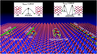
Extended line defects in two-dimensional (2D) materials can play an important role in modulating their electronic properties. During the experimental synthesis of 2D materials, line defects are commonly generated at grain boundaries between domains of different orientations. In this work, twelve types of line-defect structures in single crystalline phosphorene are examined by using first-principles calculations. These line defects are typically formed via migration and aggregation of intrinsic point defects, including the Stone–Wales (SW), single or double vacancy (SV or DV) defects. Our calculated results demonstrate that the migration of point defects in phosphorene is anisotropic, for instance, the lowest migration energy barriers are 1.39 (or 0.40) and 2.58 (or 0.49) eV for SW (or SV) defects in zigzag and armchair directions, respectively. The aggregation of point defects into lines is energetically favorable compared with the separated point defects in phosphorene. In particular, the axis of line defects in phosphorene is direction-selective, depending on the composed point defects. The presence of line defects effectively modulates the electronic properties of phosphorene, rendering the defect-containing phosphorene either metallic or semiconducting with a tunable band gap. Of particular interest is the fact that the SV-based line defect can behave as a metallic wire, suggesting a possibility to fabricate a circuit with subnanometer widths in the semiconducting phosphorene for nanoscale electronic application.


 Please wait while we load your content...