
 Open Access Article
 This Open Access Article is licensed under a
 Creative Commons Attribution 3.0 Unported Licence
The effect of atomic disorder at the core–shell interface on stacking fault formation in hybrid nanoparticles†
Shai
Mangel
a,
Lothar
Houben
bc and
Maya
Bar Sadan
 *a
*a
aDepartment of Chemistry, Ben-Gurion University of the Negev, Beer-Sheva, Israel. E-mail: barsadan@bgu.ac.il
bPeter Grünberg Institut 5 and Ernst Ruska-Centre for Microscopy and Spectroscopy with Electrons, Forschungszentrum Jülich GmbH, 52425 Jülich, Germany
cDepartment of Chemical Research Support, Weizmann Institute of Science, Rehovot, Israel
First published on 14th September 2016
Abstract
On the atomic scale, the exact engineering of interfaces affects the overall properties of functional nanostructures. One factor that is considered both fundamental and practical in determining the structural features of interfaces is the lattice mismatch, but zooming into the atomic scale reveals new data, which suggest that this paradigm should be reconsidered. Here, we used advanced transmission electron microscopy techniques to image, with atomic resolution, the core–shell interfaces of a strain-free system (CdSe@CdSe) and of a strain-induced system (CdSe@CdS). Then, we analyzed the pattern of stacking fault formation in these particles and correlated the location of the stacking faults with the synthetic procedure. We found that, in the strain-free system, the formation of stacking faults is substantial and the faults are located mostly at the core–shell interface, in a pattern that was surprisingly similar to that observed in the strain-induced system. Therefore, we conclude that the formation of faults within the nanoparticles results mainly from the interaction between the last atomic layer and the growth solution, and it is only weakly correlated with lattice mismatch. This finding is important for the design of defect-engineering in multi-step syntheses.
Introduction
Nanoscience has already explained many intriguing physical properties, but certain nano-scale phenomena, and their associated unknowns, are only now being unraveled by studying the atomic scale, wherein single-atom movements and displacements exert large effects. In the synthesis of nanoparticles, one specific problem that arises during growth, and which is correlated with the degradation of the optical quality of the nanoparticles,1 is the formation of stacking faults (SFs), in which an entire row of atoms within the particle crystallizes in a second phase. The sensitivity of the optical properties to atomic-scale changes has been demonstrated in CdSe@CdS nanoparticles, in which changing the dimensions of the core and shell affects the optical resonances of the structure.2–4 It has been shown that the fingerprint optical response of single CdSe@CdS structures is sensitive to even small changes in the homogeneity and thickness of the shell alone,3 and that SFs at the core–shell interface are detrimental to efficient emission because they act as physical trap sites, which enhance non-radiative recombination.1Despite their importance in determining the optical quality of the nanostructures, the current knowledge regarding the formation of SFs is insufficient. Common knowledge has correlated SF formation at the core–shell interface with crystallographic lattice mismatch, such that the difference in lattice parameters presumably results in strained interfaces and in the occurrence of defects. Current synthetic processes are designed according to this view and rely on the bulk properties of the materials, while disregarding the actual atomic-scale processes at the growth front.
Unfortunately, characterizing batch samples of suspended nanoparticles for prospective, practical applications5–7 is problematic, as such samples comprise ensembles of individual particles that slightly differ from one another on the atomic level, forming sub-populations that have different properties.8 As a result, our in-depth understanding of the different growth mechanisms is hindered.
To address this problem, we used advanced transmission electron microscopy (TEM) techniques to analyze the location and distribution of SFs within core–shell nanoparticles. Analyzing the differences in SF formation between a strain-free system and a strain-induced system revealed that the pattern of SF formation is independent of the lattice mismatch. Thus, we conclude that SF formation results from an inherent disorder in the outer layers of the cores, which is frozen once the core synthesis is concluded. Therefore, the structure of the interface between the core and shell is controlled by kinetic factors, rather than by thermodynamic ones.
Results
The CdSe cores were synthesized as described previously by Amirav et al.9 Following synthesis, four additional layers of the CdS shell were deposited by using a modification of the thermal cycling method, in which each cycle is intended to grow a single atomic layer to ensure an optimized interface.10,11 To synthesize the CdSe@CdSe nanoparticles, an additional step was taken, in which, after a 3 min growth stage, the reaction solution was cooled down to 330 °C and a precursor solution, which contained the reactants necessary for the deposition of four atomic layers, was injected into the growth solution to form a thick shell. The CdSe@CdS nanocrystals were 6.80 nm in diameter and had an aspect ratio of 1.20, and the CdSe@CdSe nanocrystals were 6.50 nm in diameter and had an aspect ratio of 1.73.Standard ensemble characterization methods, including photoluminescence, UV-Vis absorbance, and powder X-Ray diffraction (XRD), were used to characterize the optical and structural properties of the CdSe@CdSe and CdSe@CdS samples. The optical spectra of both samples were compared with those of the CdSe cores, which were used as a reference. A red shift relative to the CdSe cores was clearly observed in the photoluminescence and absorbance spectra of both samples (Fig. 1). In the CdSe@CdSe sample, the “core” and “shell” were made from the same material; therefore, no heterojunction was present and the shift must have originated solely from the increase in the size of the nanocrystals, which decreased the confinement of the charge carriers. In the CdSe@CdS heterostructures, the shift was due to a combination of two factors: an increase in the size of the nanocrystals and a large valence band offset, which resulted from the addition of CdS. Consequently, despite the similar size of the two nanoparticles, the CdSe@CdSe nanoparticles exhibited a greater red shift than the CdSe@CdS sample.
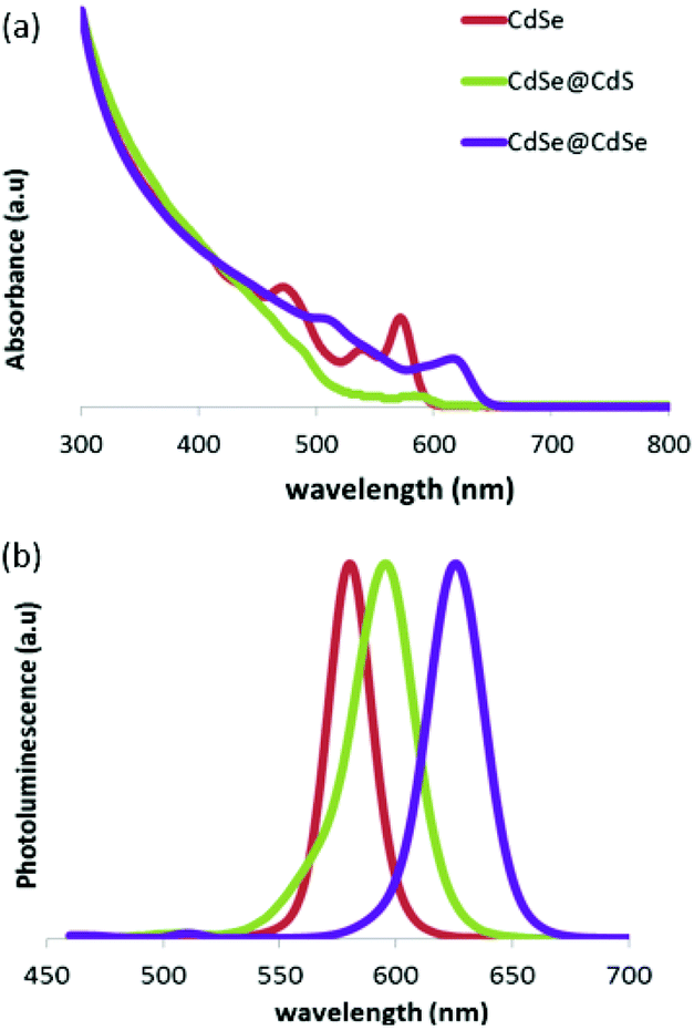 | ||
| Fig. 1 Absorbance (a) and photoluminescence (b) spectra of CdSe cores (red), a CdSe@CdS sample (green), and a CdSe@CdSe sample (purple). The photoluminescence excitation wavelength was 440 nm. | ||
The powder XRD diffraction patterns of all three samples showed an overall hexagonal symmetry pattern (Fig. 2). According to the standard analysis method introduced by Murray et al.,12 an attenuation of the ratio of the (103) peak to its adjacent (110) and (112) peaks is strongly correlated with the presence of numerous SFs within the nanocrystals. In the present study, the CdSe@CdSe sample exhibited a much stronger attenuation of the (103) peak relative to its adjacent peaks, compared with the CdSe@CdS sample. Therefore, more SFs were detected in the strain-free CdSe@CdSe system than in the strain-induced CdSe@CdS, indicating that the crystallographic lattice mismatch between the core and shell was not the dominant factor underlying SF formation. The observed shift of the CdSe@CdS reflections to higher angles is attributed to the smaller lattice parameters of the CdS lattice.
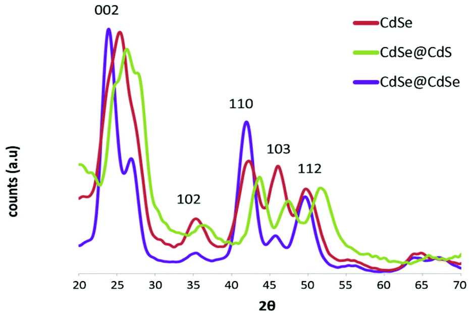 | ||
| Fig. 2 Powder XRD diffractograms of CdSe cores (red), a CdSe@CdS sample (green), and a CdSe@CdSe sample (purple). All graphs were normalized to the overall signal. | ||
Complementary direct quantitative analysis of the TEM images of both samples provided additional insights. Using aberration-corrected TEM at low voltages, a series of images were acquired in different defocus values and were used to reconstruct the phase of the electron wavefunction at the exit-plane of the sample (see Experimental procedures in the ESI†). The result of this analysis was a phase image (similar in appearance to the raw images), which provided an improved signal-to-noise ratio, elimination of artifacts due to optical lens aberrations, and a quantitative image in which the brighter intensity corresponds almost linearly to the electrostatic potential, which is related to the mass of the atoms. To obtain the information required to construct the model, the wavefunctions of several dozen CdSe@CdSe and CdSe@CdS particles were reconstructed, and their phases retrieved.
The reconstructed phase images allowed us to detect the SFs along the c-axes of the particles (Fig. 3a and b), which is the growth direction. Furthermore, it allowed us to assign the polarity of the nanocrystals by differentiating the Cd columns from the Se columns, based on the intensity.11,13,14 As the size of the original CdSe cores was known, we determined the length of the shell on both sides of the core and then divided the remaining core length into four equal sections, starting at the Cd-terminated facet and ending at the chalcogen-terminated facet (Fig. 4a). It had been previously concluded that CdSe-based nanostructures with a wurtzite phase show a well-defined unidirectional growth from the Cd-terminated facet to the more energetically active chalcogen-terminated facet.14 The two edge sections correspond to the shell area, and the four internal sections divide the core region into four quarters. The collected statistical data on the SF location were then used to construct a histogram, which compares the SF occurrence within the two samples (Fig. 4b).
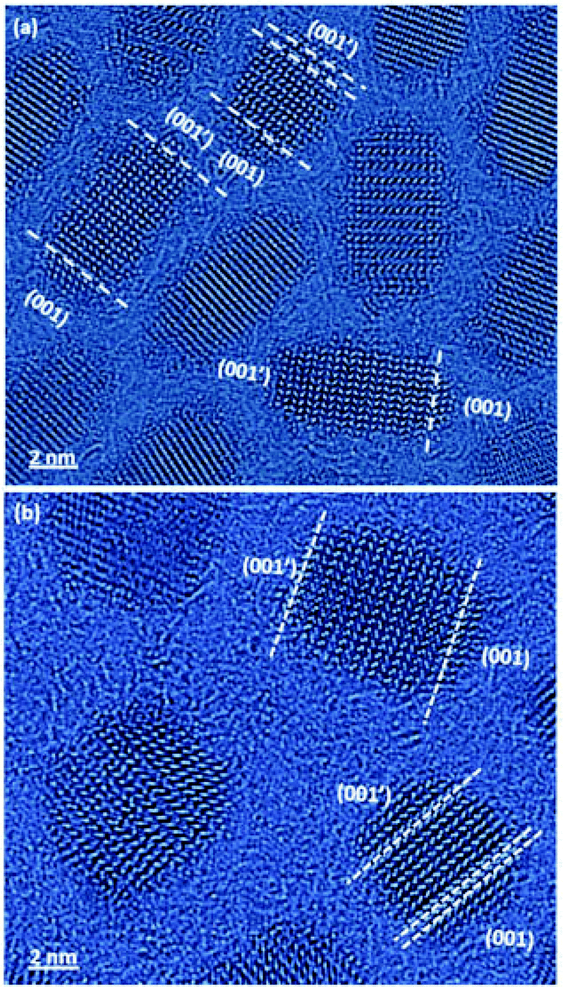 | ||
| Fig. 3 Phase images of core–shell CdSe@CdSe (a) and CdSe@CdS particles (b), showing the assignment of polarity and the identification of stacking faults. | ||
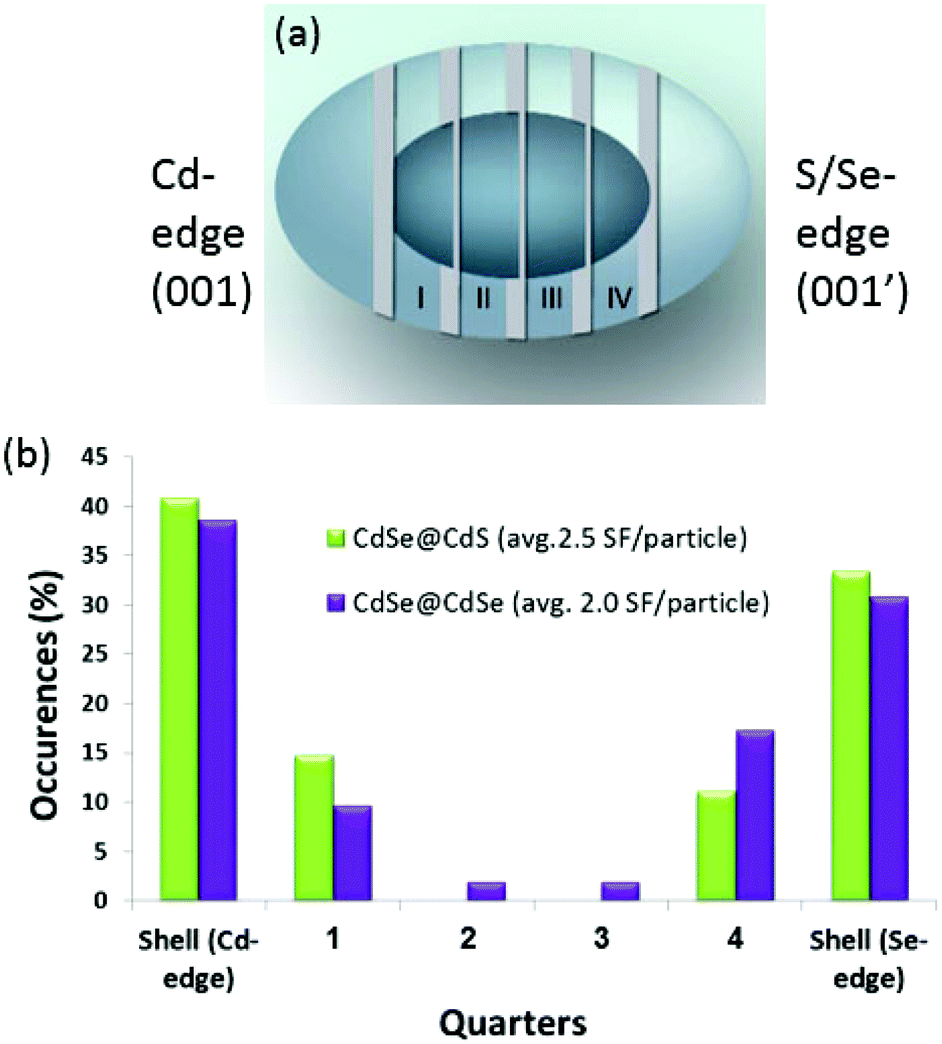 | ||
| Fig. 4 Analysis of stacking fault distribution. The samples were divided into 6 sections along the main growth direction of the particles (a). The histogram (b) shows a comparison between the occurrence of stacking faults in the CdSe@CdS sample (green) and in the CdSe@CdSe sample (purple). In each sample, 30–35 particles were analyzed. | ||
In strain-free systems, such as in the homogeneous CdSe@CdSe samples, adding layers of the same material under the same conditions should not cause additional SF formation. However, in our experiment, the CdSe@CdS sample showed 2.5 SFs per particle (as expected, given the 4% lattice mismatch between the core and the shell) and the CdSe@CdSe sample showed a similar ratio (2.0 SFs per particle) despite the 0% core–shell lattice mismatch (Fig. 4b). Moreover, the SF distribution was highly similar between the two samples, with a distinct increase in the SF concentration at the core–shell interface.
Our analysis also revealed SFs in the cores of the CdSe@CdSe samples, but not in those of the CdSe@CdS samples. We attribute this difference to the different synthetic procedures of the two samples; whereas the synthesis of the CdSe@CdS samples employed the thermal cycling method, in which the temperature of the growth solution is raised intermittently to produce an ordered deposition of the CdS shells, the CdSe@CdSe samples did not undergo such thermal treatment and, therefore, the relaxation of the inner structure was hampered and the SFs within the core of the particles were preserved.
To test whether the thermal treatment of CdSe@CdS samples was indeed responsible for the lack of SF formation in the cores of the structures, we conducted a control experiment, in which CdSe particles were synthesized as described above, but an aliquot of the sample was then subjected to the same thermal cycle used to prepare the CdSe@CdS sample. The XRD diffractograms of the two samples (Fig. 5) revealed that, indeed, the attenuation of the (103) peak relative to its two adjacent peaks was much more pronounced (indicating the presence of SFs) in the as-synthesized sample than in the thermal cycle-treated sample, which exhibited an almost perfect wurtzite structure.
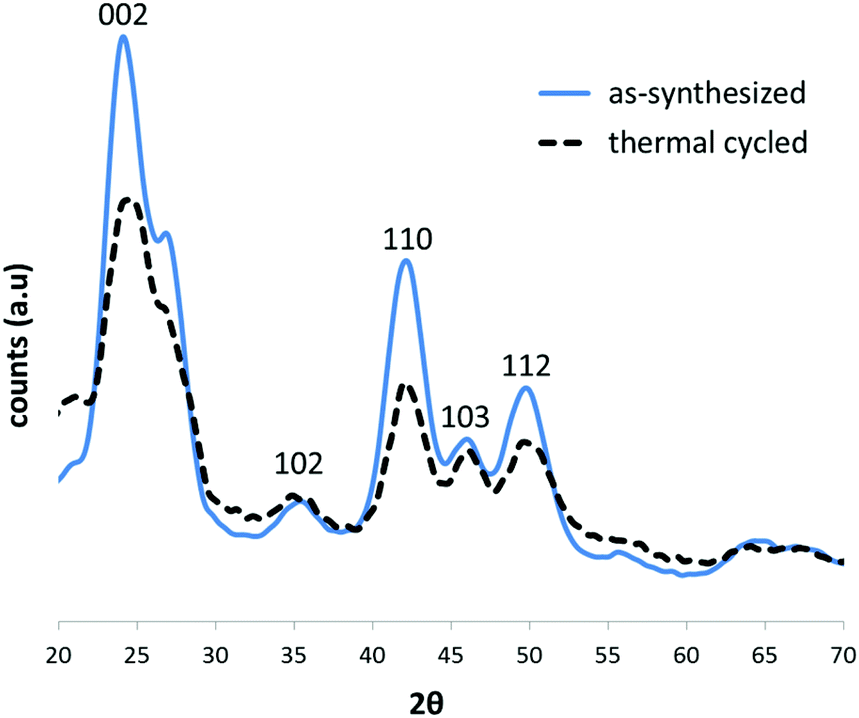 | ||
| Fig. 5 XRD diffraction patterns of an as-synthesized CdSe sample (solid blue line) and of a similar sample that underwent thermal cycling (dashed black line), and was, therefore, annealed. All graphs were normalized to the overall signal. | ||
Our results indicate that the crystallographic lattice mismatch between the core and shell of inorganic nanoparticles plays only a minor role in the formation of SFs in solution-prepared nanocrystals. Rather, we propose that the atomic reconstruction of the surface of the nanocrystal prior to shell deposition is a dominant factor, which plays a crucial role in SF formation. Previous studies have shown that more defective surfaces of CdSe cores promote better epitaxial interfaces when a CdS shell is deposited and then annealed, yielding, counterintuitively, an almost unity quantum yield of the CdSe@CdS nanoparticles.15 In contrast, when the surface of the CdSe core contains less structural defects, the annealing process of the hybrid material is less successful and the optical properties are inferior.15
We suggest that a variety of interactions occurs at the surface of the particles during the stage of shell deposition, which prevents surface atoms from reaching their thermodynamic equilibrium position. In addition to the inherent atomic-scale disorder at the outer layers of the particle, these interactions involve the capping ligands or other species from the growth solution. The presence of such atomic-scale surface disorder is demonstrated in Fig. 6, in which a CdSe@CdS particle (taken from a different batch from the ones used in the above experiments) demonstrates two crystallographic phases: the original hexagonal wurtzite (on the left) and a cubic zinc blende (on the right), which is situated at the growth front. Overlaid on the image are four circles, which denote where the atomic-scale disorder is present in addition to the phase transition from wurtzite to zinc blende. In circle 1, one Cd–Se column pair is inclined relative to the crystal; in circle 2, the Cd–Se column pair is, in fact, a trio of dots, showing probable interstitial or displaced atoms; in circle 3, only one of the Cd–Se columns is seen; and in circle 4, the edge of the crystal is shown, wherein the column structure is absent and disorder prevails.
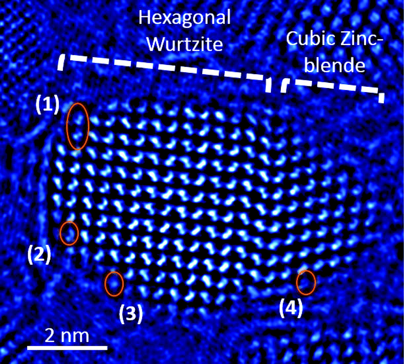 | ||
| Fig. 6 A phase image of a CdSe@CdS particle. The orange circles indicate irregularities in the crystal structure of the particle at the outer layers. See text for details. | ||
Conclusions
We have shown, by using CdSe particles as a model, that the formation of stacking faults in spherical core–shell particles is not driven by the crystallographic lattice mismatch between the shell and core. Rather, the surface reactions and processes, which are mainly effected by kinetic factors, appear to play a major role in the formation of stacking faults, as demonstrated by the formation of stacking faults even at the core–shell interface of the strain-free system.Acknowledgements
This study was supported by The Israeli Centers of Research Excellence (I-CORE) program (Center No. 152/11), by an Israel Science Foundation (ISF) grant No. 475/12, by the Adelis Fund, and by the European Union Seventh Framework Program, under Grant Agreement 312483-ESTEEM2 (Integrated Infrastructure Initiative-I3). M. B. S. appreciates support from Dr Dmitri Mogilyanski from the Ilse Katz Institute for Nanoscale Science Technology in Ben-Gurion University of the Negev.References
- N. J. Orfield, J. R. McBride, J. D. Keene, L. M. Davis and S. J. Rosenthal, ACS Nano, 2015, 9, 831–839 CrossRef CAS PubMed.
- J. Van Embden, J. Jasieniak and P. Mulvaney, J. Am. Chem. Soc., 2009, 131, 14299–14309 CrossRef CAS PubMed.
- N. J. Borys, M. J. Walter, J. Huang, D. V. Talapin and J. M. Lupton, Science, 2010, 330, 1371–1374 CrossRef CAS PubMed.
- X. Chen, Y. Lou, A. C. Samia and C. Burda, Nano Lett., 2003, 3, 799–803 CrossRef CAS.
- D. K. Kim, Y. Lai, B. T. Diroll, C. B. Murray and C. R. Kagan, Nat. Commun., 2012, 3, 1216 CrossRef PubMed.
- J. Song and H. Zeng, Angew. Chem., Int. Ed., 2015, 54, 9760–9774 CrossRef CAS PubMed.
- Y. Shirasaki, G. J. Supran, M. G. Bawendi and V. Bulovic, Nat. Photonics, 2013, 7, 13–23 CrossRef CAS.
- S. Majumder, I.-T. Baeb and M. M. Maye, J. Phys. Chem. C, 2014, 2, 4659–4666 CAS.
- L. Amirav and A. P. Alivisatos, J. Phys. Chem. Lett., 2010, 1, 1051–1054 CrossRef CAS.
- B. Blackman, D. M. Battaglia, T. D. Mishima, M. B. Johnson and X. Peng, Chem. Mater., 2007, 19, 3815–3821 CrossRef CAS.
- S. Mangel, E. Aronovitch, A. N. Enyashin, L. Houben and M. Bar-Sadan, J. Am. Chem. Soc., 2014, 136, 12564–12567 CrossRef CAS PubMed.
- C. B. Murray, D. J. Norris and M. G. Bawendi, J. Am. Chem. Soc., 1993, 115, 8706–8715 CrossRef CAS.
- S. Mangel, L. Houben and M. Bar-Sadan, Cryst. Growth Des., 2015, 15, 3114–3118 CAS.
- G. Bertoni, V. Grillo, R. Brescia, X. Ke, S. Bals, A. Catellani, H. Li and L. Manna, ACS Nano, 2012, 6, 6453–6461 CrossRef CAS PubMed.
- A. Saha, K. V. Chellappan, K. Narayan, J. Ghatak, R. Datta and R. Viswanatha, J. Phys. Chem. Lett., 2013, 4, 3544–3549 CrossRef CAS.
Footnote |
| † Electronic supplementary information (ESI) available. See DOI: 10.1039/c6nr04867f |
| This journal is © The Royal Society of Chemistry 2016 |