
 Open Access Article
 This Open Access Article is licensed under a Creative Commons Attribution-Non Commercial 3.0 Unported Licence
Electrostatically driven drumhead resonators based on freestanding membranes of cross-linked gold nanoparticles†
Hendrik
Schlicke‡
,
Clemens J.
Schröter‡
and
Tobias
Vossmeyer
*
Institute of Physical Chemistry, University of Hamburg, Grindelallee 117, 20146 Hamburg, Germany. E-mail: tobias.vossmeyer@chemie.uni-hamburg.de; Fax: +49 40 42838 3452; Tel: +49 40 42838 7069
First published on 11th July 2016
Abstract
Freestanding, nanometer-thin membranes of alkanedithiol cross-linked gold nanoparticles represent elastic, mechanically robust and electrically conductive materials, which are interesting for the fabrication of novel nano- and microelectromechanical devices. In this work we present the first electrostatically driven drumhead resonators based on such nanoparticle membranes. These circular membranes have a thickness of 33 to 52 nm, a diameter of either 50 μm or 100 μm, and are equally spaced from their back electrode by ∼10 μm. Using an interferometric nanovibration analyzer various vibrational modes with resonance amplitudes of up to several 100 nm could be detected when the membranes are excited by applying AC voltages (<30 V) with drive frequencies of up to 2 MHz. Further, spatial amplitude distributions of different vibrational modes could be imaged. The devices showed fundamental resonance frequencies in the high kHz range and quality factors Q up to ∼2000. Finally, vibrational spectra and observed mode patterns could be well interpreted using the theory for a clamped circular membrane with negligible bending stiffness. Our findings mark an important step towards the integration of freestanding gold nanoparticle composite membranes into electromechanical devices with various applications, such as novel types of pressure or mass sensors.
Introduction
Resonators perform as fundamental device components in numerous microelectromechanical systems (MEMS). Today they are used e.g. in accelerometric and gyroscopic sensors. During the last two decades research and development have been focused on shrinking the dimensions of electromechanical devices yielding so-called nanoelectromechanical systems (NEMS) with critical feature sizes in the nanometer range.1 Accordingly, interest has grown in the incorporation of nanometer-thin freestanding membranes as functional materials into these devices. Current studies demonstrate the applicability of NEMS and MEMS resonators consisting of such membranes for sensing pressure2 or small forces and masses with extremely high sensitivity.3Besides conventional silicon-based materials, novel 2D and 3D thin films are currently being investigated concerning their integration into resonator devices. Lightweight 2D materials can for example be used for the fabrication of resonators with high resonance frequencies and high mass sensitivities. Bunch et al. demonstrated the fabrication of electromechanical resonators based on graphene membranes with thicknesses varying from a single atomic layer up to 75 nm with fundamental resonant frequencies in the range of 1–170 MHz, actuated by electrical or optical modulation.4 With amorphous diamond-like carbon another modification of carbon was used for resonator fabrication, recently.5 Also black phosphorus6 and transition metal dichalcogenides, such as single7 or multilayer8 MoS2 as well as TaO2,9 were integrated as functional materials. Zhang et al. reported on resonators fabricated from carbon nanomembranes obtained by self-assembly and subsequent interlinkage of organic molecules.10
In addition to inorganic and organic materials, freestanding membranes of nanoparticle/organic composites have gained attention during recent years, offering versatile tunability of application specific properties as well as convenient ink-based film fabrication by printing11,12 or spin-coating,13 and transfer procedures such as microcontact printing.14 For example, Tsukruk and coworkers reported on the fabrication of gold nanoparticle (GNP)/polymer composite membranes and, using external piezoelectric actuation, analyzed their resonance frequencies which were found in the kHz range.15 Further, Jaeger and co-workers reported on the fabrication of freestanding 2D membranes of self-assembled monolayers from monothiol capped gold nanoparticles and demonstrated their application as drumhead resonators with resonance frequencies in the low MHz range. These resonators were also driven by external piezoelectric actuators or thermal excitation.16
Thin films and membranes consisting of GNP/polymer composites or GNPs stabilized with long-chain monothiols are usually insulating or exhibit rather low electric conductivity. In contrast, fairly good and adjustable conductivities can be achieved by assembling GNPs with short-chain ligands and by cross-linking the particles with short dithiols. So far, however, most work on conductive GNP composites has been mainly focused on substrate-supported thin films and their applications as chemiresistors17 or resistive strain gauges18–21 and investigations of freestanding membranes consisting of such conductive GNP composites have started only recently. In this context, the emphasis of our present work is on freestanding, dithiol cross-linked GNP membranes and their potential applications in various types of MEMS/NEMS devices. Their conductivity22 as well as other properties, e.g. elasticity, optical absorption23 and chemical affinity17,20 can be adjusted by the proper choice of linker molecules and particle sizes and shapes. The mechanical stability of dithiol cross-linked GNP films24 allows them to be lifted off their initial substrates and deposited onto a variety of 3D microstructures to produce devices based on freestanding GNP membranes.13 For example, in a recently published study we demonstrated the application of freestanding, organically cross-linked GNP membranes as resistive pressure gauges.25 Until now, resonators built from gold nanoparticle composites have been thermally excited or externally driven by piezoelectric actuators. Electrostatic actuation, which is a widespread principle in MEMS and NEMS has not been applied so far. In an earlier study we demonstrated the static deflection of freestanding GNP membranes by applying DC voltages.26 Here, we fabricated and characterized the first electrostatically driven MEMS/NEMS resonators with high Q factors based on freestanding membranes of 1,6-hexanedithiol (6DT) cross-linked GNPs. By applying this versatile principle no external piezo actuators are necessary and the fabrication and integration of such devices are significantly simplified.
Experimental
Synthesis of gold nanoparticles
1-Dodecylamine capped GNPs were used for membrane fabrication in this study. The particles were synthesized following a procedure by Leff et al.27Preparation of cross-linked GNP films
6DT cross-linked GNP films were fabricated as described in an earlier publication.13 In this study the process was modified with regard to the pre-treatment procedure for the glass substrates. Here, the substrates were treated in an oxygen plasma (SPI supplies plasma prep II) prior to deposition. Afterwards, the substrates were placed on a spin-coater and rotated at a constant rate of 3000 rpm. Firstly, 100 μL of a 7.4 mM solution of 6DT in toluene were applied to the rotating substrate two times. After this pre-treatment, a GNP layer was deposited by applying 10 μL of the ∼90 μM GNP stock solution in n-heptane to the substrate. Afterwards, 10 μL of a 7.4 mM solution of 6DT in methanol were applied two times in order to cross-link the GNPs. The GNP deposition and cross-linking steps represent one deposition cycle. GNP films investigated in this study were fabricated by applying either 3 (A, B) or 5 (C, D, E) deposition cycles. Between all applications of the solutions, a delay of ∼30 s was maintained. Eventually, the GNP films were immersed in a methanolic solution of 6DT (7.4 mM) overnight and subsequently rinsed with acetone and dried in a nitrogen flow.Fabrication of the 3D electrode microstructures
3D electrode microstructures were prepared following a multi-step optical lithography process, similar to that described in detail in our previous work.26 15 × 15 mm2 pieces of a silicon wafer with a 300 nm SiO2 layer (Addison, 〈100〉 ± 0.5°, CZ-n-Sb, 300 nm ± 5%, 0.005–0.025 Ω cm) served as substrates. All photolithography steps were carried out under yellow light.The back electrodes (BEs) were structured by depositing a sacrificial layer of an AZ nLOF 2070_3.5 μm negative photoresist for 60 s with 150 rps using a spin coater (K.L.M. SCC-200). After deposition, the photoresist was soft-baked on a hotplate for 180 s at 100 °C. Once the sample had cooled down to ambient temperature, it was irradiated with UV light through a patterned photomask using a Karl Suss MJB-3 mask aligner. The photoresist was baked post exposure for 60 s at 120 °C. After the sample cooled down to ambient temperature the photoresist was developed by immersion in an AZ 726 MIF developer (AZ Electronic Materials) for 60 s. The substrate was then rinsed with demineralized water and dried in a nitrogen flow. Onto this sacrificial layer multiple electrode layers were deposited. In order to increase adhesion and to remove the remaining organic material in the resist-free areas the samples were cleaned for 2 min (Harrick Plasma, PDC-002) in an oxygen plasma. Using thermal evaporation (oerlikon leybold vacuum UNIVEX 350-G or Pfeiffer Classic 250 Vacuum Evaporation System), layers of titanium (∼10 nm) and gold (∼40 nm) were deposited onto the sample. In an additional step a carbon layer (∼10 nm) was deposited on top in order to reduce the reflectivity of the electrodes. The carbon evaporation was carried out by applying a current of >25 A to a twisted carbon fiber of ∼1.5 cm length and 0.4 g m−1 in vacuum. In the following lift-off step the sample was immersed in TechniStrip NI555 (TECHNIC) at 70 °C for 10 min. If necessary, the sample was sonicated (Bandelin Sonorex) for a maximum of 10 s to finalize the lift-off. Afterwards the samples were rinsed with acetone and demineralized water and dried in a nitrogen flow.
On top of the BEs a SU-8 2015 (MicroChem) photoresist layer was spin-coated for 60 s at 100 rps. This resulted in a SU-8 layer with a thickness of ∼10 μm. After deposition, the photoresist was soft-baked for 180 s at 95 °C. Once the sample had cooled down to ambient temperature, it was irradiated with UV light through a patterned photomask and a 360 nm long pass filter (Omega Optical Inc. PL-360 LP). The photoresist was baked post exposure for 240 s at 95 °C. After the sample cooled down to ambient temperature the photoresist was developed by immersion in an mr-Dev600 (Micro Resist Technology) developer for 180 s under agitation. The substrate was then rinsed briefly with a fresh developer and 2-propanol and dried in a nitrogen flow. Finally the sample was hard baked for 20 min on a ramping hot plate starting from 120 °C to 200 °C in the first 10 min. Commonly, the maximum deviation of the SU-8 cavity diameter from the targeted values of 50 μm and 100 μm was in a range of ±2 μm.
For the top electrode (TE) a sacrificial layer was structured on top of the SU-8 structures. A layer of an AZ nLOF 2070_3.5 μm photoresist was spin-coated for 60 s at 68 rps. After deposition the photoresist was soft-baked for 90 s at 120 °C. Once the sample cooled down to ambient temperature an additional layer of the AZ nLOF 2070_3.5 μm photoresist was spin-coated for 60 s at 68 rps and soft baked for 180 s at 120 °C. The second coating step was conducted to ensure a complete coverage of the 3D structure with the photoresist. Afterwards, UV light exposure was carried out using a patterned photomask. The photoresist was baked post exposure for 60 s at 120 °C. After the sample cooled down to ambient temperature the photoresist was developed by immersion in an AZ 726 MIF developer (AZ Electronic Materials) for 120 s. The substrate was then rinsed with demineralized water and dried in a nitrogen flow. In order to increase adhesion and remove the remaining organic material in the resist-free areas, the samples were cleaned for 2 min (Harrick Plasma, PDC-002) in an oxygen plasma. For the TEs a single gold layer (∼40 nm) was deposited using thermal evaporation. In the following lift-off step the sample was immersed in TechniStrip NI555 (TECHNIC) at 70 °C for ∼15 min. If necessary, the samples were sonicated (Bandelin Sonorex) for ∼5 s. Finally, the samples were rinsed with acetone and demineralized water and dried in a nitrogen flow.
Results and discussion
Fabrication of resonator devices
Fig. 1a depicts a schematic view of an exemplary device. A GNP membrane was deposited onto a microstructure, spanning a circular microcavity. A gold top electrode, used as the signal ground, makes electrical contact with the membrane. In close proximity below the freestanding membrane another gold (back) electrode is arranged. Application of an AC signal to the latter electrode results in a time-dependent potential difference and hence attractive coulomb forces driving oscillations of the membranes.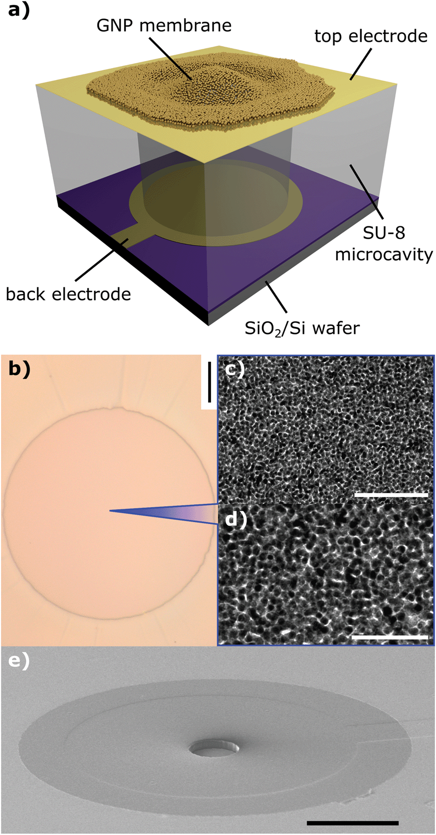 | ||
| Fig. 1 (a) Schematic of a GNP membrane resonator. (b) An optical micrograph of a device. The image shows a 6DT cross-linked GNP membrane deposited onto a circular 100 μm cavity. Scale bar: 20 μm. (c, d) Transmission electron micrographs of a representative 6DT cross-linked gold nanoparticle membrane transferred to a carbon-coated TEM substrate. Scale bars: (c) 100 nm and (d) 50 nm. (e) A scanning electron micrograph of an electrode substrate featuring a 50 μm wide cavity, as used for resonator fabrication. Scale bar: 100 μm. | ||
The microsystem comprises a layered Ti/Au/carbon back electrode (∼10 nm/∼40 nm/∼10 nm, respectively), which was lithographically fabricated on an oxidized silicon wafer (300 nm thermal oxide) by vacuum evaporation and a subsequent lift-off process. Here, the carbon layer yields a lower reflectivity of the electrode, which is favorable for the interferometric measurements conducted in this study (see below). Onto the back electrode, a ∼10 μm thick layer of SU-8, a non-conductive epoxy photoresist, was deposited via spin-coating. Using standard photolithography, cylindrical cavities of 50 μm and 100 μm diameter were structured into the SU-8 layer. In the final lithography step, a top electrode (Au, ∼40 nm thickness) was deposited onto the SU-8 layer and structured by applying a lift-off process, analogously to the fabrication of the back electrode. Each microsystem contains an array of 4 × 4 devices (see the ESI, Fig. S5†). While the top electrode is continuous, each device features an individual back electrode, which enables addressing the resonators one-by-one. A scanning electron micrograph of an as-fabricated electrode microstructure featuring a 50 μm wide cylindrical cavity is depicted in Fig. 1e.
6DT cross-linked GNP films were fabricated following our standard spin-coating based procedure. Alternately a solution of dodecylamine-capped GNPs (core diameter: 3.6 ± 0.6 nm) in n-heptane and a methanolic solution of 6DT were deposited onto glass substrates, as described earlier. By repeating these deposition steps, the thickness of the resulting GNP thin film could be adjusted.13 UV/vis absorption spectroscopy of the films showed a typical red shift of the GNP surface plasmon resonance absorption band due to the close packing of the particles in the material. Also the current–voltage characteristics of the films were recorded and ohmic behavior with a conductivity of 0.1 S cm−1 was observed, which is in good agreement with earlier studies.13,23,26 The thickness of the GNP films was determined by AFM measurements as reported earlier.13 See the ESI† for respective absorbance spectra, current–voltage data, topographic AFM data of the as-deposited films, a representative transmission electron micrograph as well as a size histogram of the GNP batch used for film fabrication. Fig. 1c and d show transmission electron micrographs of a GNP membrane transferred to a carbon-coated TEM substrate. The granular structure of the membrane with grain sizes in the nanometer regime can clearly be identified.
Following deposition, the GNP films were lifted off their initial glass substrates by flotation on demineralized water. After a few days the films could be detached from their substrates by careful immersion of the substrates into the aqueous phase making the membranes to free-float at the liquid–air interface. Subsequently, the membranes were skimmed using the electrode microstructures. An optical micrograph of a 6DT cross-linked GNP membrane transferred to a microstructure featuring a 100 μm wide cylindrical cavity is provided in Fig. 1b. The structures were allowed to dry and, thereafter, fixed on custom-designed printed circuit boards and connected by wire bonding.
Vibrational spectra
The fabricated resonator devices were placed into a custom-built vacuum cell (pressure 10−1 to 10−2 mbar) mounted on an x,y-translation stage. Fig. 2 depicts the setup used for device characterization. The membrane actuators were driven by the voltage signal of a function generator (Keysight 33521B) amplified by a high voltage amplifier (Falco Systems WMA-300). Commonly the samples were excited with a sine voltage function V(t) = VDC + VAC![[thin space (1/6-em)]](https://www.rsc.org/images/entities/char_2009.gif) sin(2πfdt) in a drive frequency fd range up to 2 MHz. An offset voltage of VDC > VAC was chosen to avoid a change of the bias direction resulting in a force minimum at the zero crossing point as the operating coulomb forces F scale with the square voltage, F ∝ V2.26
sin(2πfdt) in a drive frequency fd range up to 2 MHz. An offset voltage of VDC > VAC was chosen to avoid a change of the bias direction resulting in a force minimum at the zero crossing point as the operating coulomb forces F scale with the square voltage, F ∝ V2.26
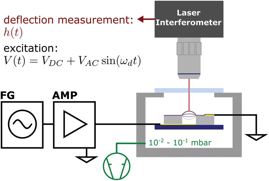 | ||
| Fig. 2 Schematic of the setup used for electrostatic resonator characterization. A sine voltage signal from a function generator (FG) amplified by a high voltage amplifier (AMP) is used to drive a resonator placed in a custom-built vacuum cell. Deflection time traces are recorded with a laser interferometer. | ||
For standard vibration spectrum acquisition (“frequency scanning” acquisition), membrane deflection time traces h(t) were recorded using an interferometer (SIOS Nanovibration Analyzer NA) at varying excitation frequencies fd. For each applied frequency, 8192 datapoints were acquired with a sample rate of 12.5 MHz. Due to its measurement principle, the SIOS Nanovibration Analyzer NA enables highly linear deflection measurements. Detailed information on the interferometric measurements are provided in the ESI.† Amplitude spectra h0(fd) = 2|C(fd)| were obtained by computing the magnitude of the vibration's Fourier component C at the respective drive frequency fd for each recorded deflection time trace. No deflection of the SU-8 layer was measured in proximity to the freestanding membranes. A detailed summary of the measurement and data processing is provided in the ESI.†
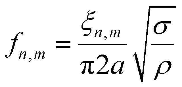
Fig. 3a shows the vibration amplitude spectrum measured in the center (x = 0, y = 0, see the inset) of a 6DT cross-linked GNP membrane (thickness: 38 ± 1 nm) spanning a 100 μm cavity, excited with a voltage signal of VAC = 5 V and VDC = 15 V. The spectrum shows a first pronounced peak at a frequency of f0,1 = 379 kHz with an amplitude of several hundreds of nanometers, which we assign to the fundamental (0,1) vibration of the membrane. For a clamped membrane under tensional stress σ, with a density ρ and negligible bending stiffness, its natural resonant frequencies in a vacuum are expected at distinct frequencies fn,m, which can be computed using eqn (1).16,28
 | (1) |
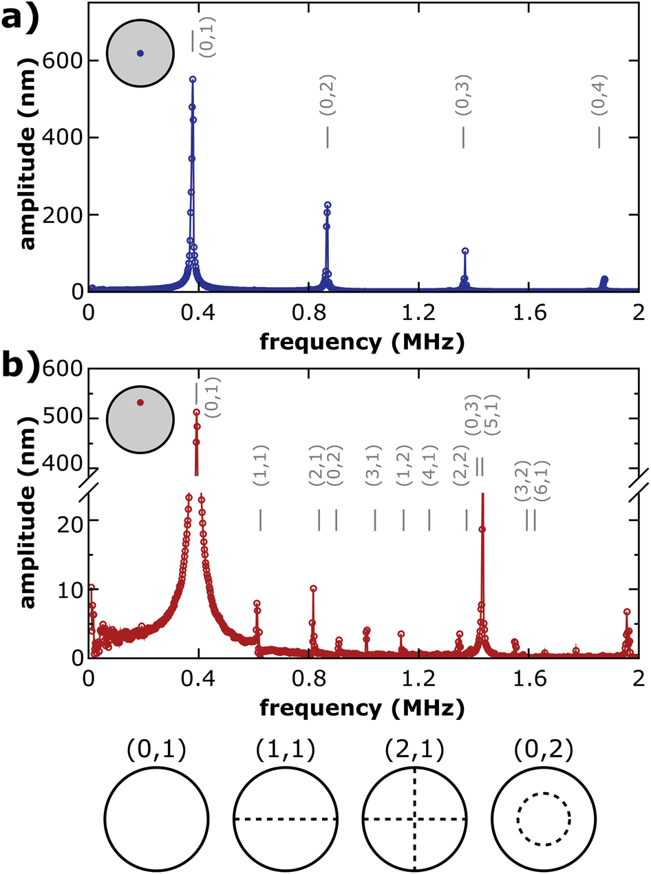 | ||
| Fig. 3 Amplitude spectra of a 100 μm diameter 6DT cross-linked GNP membrane resonator (thickness: 38 ± 1 nm) measured (a) at its center (x = 0, y = 0) and (b) off-center (x = 0, y = 25 μm). The inset schemes depict the approximate position on the membrane surface. Vertical grey lines indicate the estimated frequencies of different vibrational modes of the membrane according to eqn (1). The respective mode numbers are given as (n,m) tuples. Sketches of selected vibrational mode patterns with their characteristic nodal lines are depicted at the bottom of the figure. | ||
ξ n,m is a constant depending on the mode number and is represented by the m-th root of the n-th order Bessel function for circular membranes. The mass density of composite membranes of 6DT cross-linked ∼4 nm sized GNPs was estimated as ρ = 3.8 g cm−3 by XPS measurements, reported previously.29 Taking into account the aperture radius of a = 50 μm, a tensional stress of the membrane of σ = 9.3 MPa could be extracted. Values in the MPa range compare well with the residual stress values measured for 6DT cross-linked membranes under DC electrostatic deflection.26
Using eqn (1), the frequencies of higher vibrational modes can be estimated by taking into account the f0,1 frequency. Vibrational modes (n,m) of circular membranes are characterized by their number of nodal lines separating areas of the membranes with inversely phased oscillations. While the second index m denotes the radial mode number, which is the number of circular nodal lines (including the circumference of the membrane), the first index n denotes the azimuthal mode number, which is the number of nodal lines crossing the center of the membrane. Hence, it is expected that only (0,m) vibrational modes with non-zero amplitudes at the membrane center can be observed as in Fig. 3a. It is clearly visible that the frequencies estimated for (0,2), (0,3) and (0,4) modes agree very well with the spectral positions of amplitude maxima observed in the experiment.
Fig. 3b depicts an amplitude spectrum recorded off-center at the half radius of the resonator membrane. Just like the amplitude spectrum measured at the membrane center, the off-center spectrum also features a pronounced fundamental resonance peak. However, the peak is slightly shifted to f0,1 = 392 kHz. In general, we observed slightly shifting resonance peaks when scanning the membrane with the interferometer laser. We attribute this finding to local heating of the membrane due to laser irradiation. Based on the fundamental f0,1 resonance frequency, again the frequencies of higher modes were estimated. The spectral positions are depicted as grey vertical lines in Fig. 3b, annotated with respective mode numbers. Most of the estimated mode frequencies agree well with the peak positions found in the experiments.
The fundamental resonance frequencies f0,1 of a total of 26 devices were measured using the faster “frequency sweeping” spectrum acquisition method (see the ESI†) applying an excitation voltage signal with VDC = 5 V, VAC = 2.5 V for resonators with a diameter of 100 μm and VDC = 10 V, VAC = 5 V for resonators with a membrane diameter of 50 μm. It is worth noting that changes in the membranes’ tensional stress due to a variation of the offset voltage in the given range did not lead to significant shifts of the fundamental resonance frequency. Further, we did not find evidence for a correlation of the fundamental resonance frequency with the applied drive amplitude within the accuracy of our measurements. See the ESI† for details. In order to study the effect of different membrane thicknesses devices probed in this set of experiments comprised membranes fabricated by applying either three deposition cycles (average thickness t = 34 ± 1 nm) or five deposition cycles (average thickness t = 51 ± 1 nm). For the thicker membranes, fundamental resonance frequencies of 336 ± 28 kHz and 697 ± 53 kHz were found for the larger and smaller resonators, respectively. For the same device dimensions the thinner membranes showed f0,1 values of 376 ± 18 kHz and 735 ± 4 kHz. The resonance frequencies of the smaller resonators are approximately twice as high as the resonance frequencies of the larger resonators, as expected by theory (see eqn (1)). Further, on average somewhat higher resonance frequencies were measured for resonators built from thinner GNP membranes. This indicates that tuning of the resonance frequency is possible by adjusting the membrane thickness. Assuming a similar surface tension σt for all membranes, we attribute this finding to the lower mass of the thinner membranes. Further, we assume that the observed scattering of the resonance frequencies can be reduced by optimizing the membrane transfer process, resulting in better control of the membrane tension.
Amplitude mappings
To further confirm the assignment of the resonance frequencies to their vibrational modes, mappings of the membrane vibrations were conducted. The acquisition of amplitude and phase maps was complicated, because the resonance peaks shifted slightly when scanning the laser over the freestanding membrane area. To overcome this problem, vibration spectra were acquired at each mapping position on the membrane by computing fast Fourier transforms (FFTs) of deflection time traces recorded while exciting the samples using frequency swept sine voltages (“frequency sweeping” acquisition). Deflection amplitude maps were then computed by extracting the peak amplitude in the respective spectral regions. See the ESI† for details on the amplitude mapping procedure. Fig. 4a depicts the spatial amplitude distribution of a 100 μm diameter resonator consisting of a 52 ± 1 nm thick 6DT cross-linked GNP membrane generated by taking into account the first amplitude maximum at f0,1 of the spectra recorded at each point. The amplitude distribution shows a maximum at the membrane center which smoothly decreases towards the edges of the membrane. This is expected for the fundamental (0,1) vibration of a clamped membrane. In contrast, Fig. 4b depicts the amplitude maxima found around ∼2.3f0,1, i.e. where the (0,2) vibrational mode is expected. A circular nodal line with an amplitude minimum concentrically separating two areas with higher amplitudes is clearly visible. This is characteristic for the (0,2) vibrational mode (see the inset). It is worth noting that the mapping shows a distortion from a perfect circular appearance. This behavior is possibly caused by inhomogeneous local tensioning of the membrane. We assume that such inhomogeneities can be reduced in future by improving the transfer of the membranes onto the microcavities, which is currently carried out manually. Besides, inhomogeneous local heating of membrane sections according to the scan pattern might affect the amplitude images’ symmetry. Plotting the amplitude maxima occurring in the spectral range from 3.50f0,1 to 3.80f0,1 yielded the amplitude map shown in Fig. 4c. Here two circular nodal lines can be seen, which are characteristic for the (0,3) vibrational mode, expected at 3.60f0,1. These results unambiguously confirm the assignment of the resonance modes in the amplitude spectra.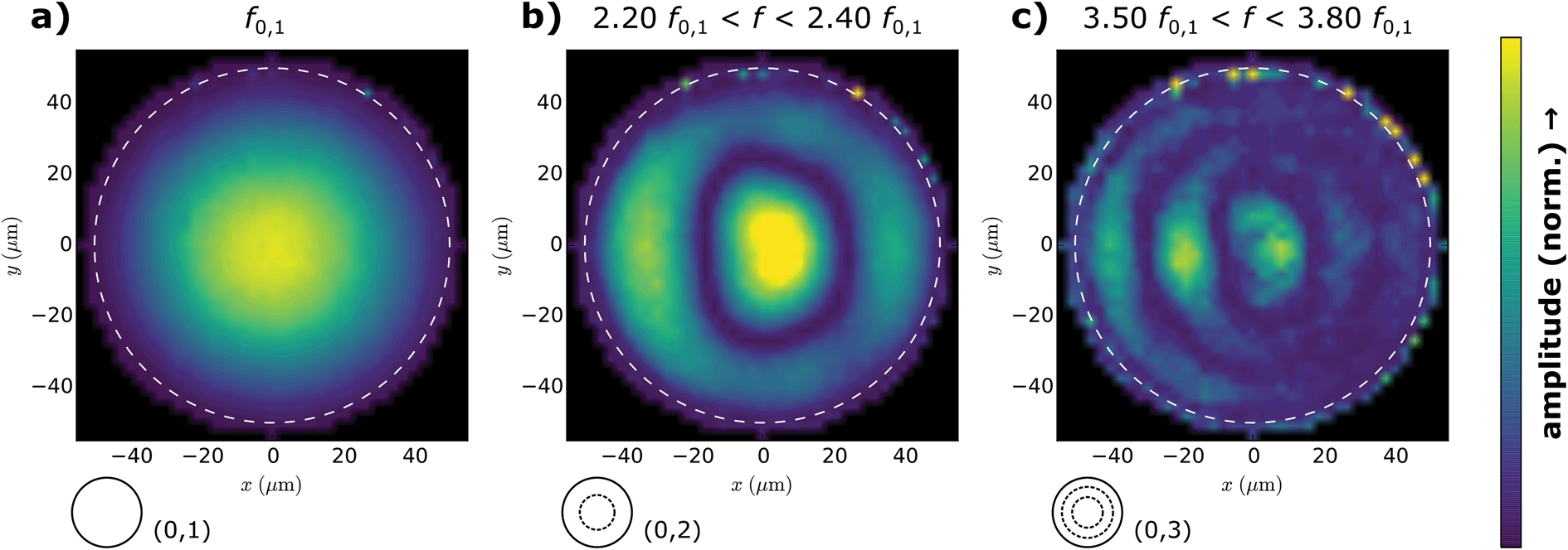 | ||
| Fig. 4 Amplitude mappings of an electrostatically driven 100 μm diameter GNP membrane resonator. The plots depict the amplitude maxima found in the frequency ranges denoted above the images (a), (b) and (c). The amplitudes are normalized in each image individually. The schemes in the lower left of the plots depict the mode numbers of membrane normal modes which are in good agreement with the observed amplitude patterns. Theoretically, the higher modes shown are expected at resonance frequencies of (b) f0,2 = 2.30f0,1 and (c) f0,3 = 3.60f0,1. Dashed white lines depict the outline of the freestanding membrane. | ||
In conclusion, the good agreement of the theoretical and experimental peak positions shows that the membranes’ dynamic behavior in a vacuum can be well-described using the model for a clamped circular membrane with negligible bending stiffness.
Ring down experiments
For determining the resonators’ quality factors Q, ring down experiments were conducted. Here, the resonators were excited at their f0,1 resonance frequency by applying a burst of 10 to 80 sine voltage cycles with VDC = 5 V and VAC = 2.5 V for 100 μm membranes. A slightly higher drive signal of VDC = 10 V and VAC = 5 V was used for the smaller 50 μm membrane resonators. Synced with the start of the excitation signal, deflection data h(t) were recorded using the interferometer. After burst excitation, the drive signal was switched off and the ring down of the membrane oscillation was monitored. A modulation of the raw deflection data due to the oscillation of the interferometer's reference mirror (∼800 Hz) was removed by Fourier transformation of the h(t) data, elimination of the low-frequency Fourier components (≤100 kHz) and back-transformation to the time-domain (see the ESI†). Afterwards, the ring down of the oscillation was fitted using eqn (2), which describes a damped harmonic oscillator. | (2) |
Here, h0 is the initial amplitude of the oscillation and ϕ denotes the phase. As indicated by eqn (3), the quality factor Q is calculated from the decay time of the oscillation τ and the oscillators resonance frequency fres, extracted as parameters of the fit.6
| Q = τπfres | (3) |
The exemplary ring down data shown in Fig. 5 were obtained by investigating a 100 μm diameter 6DT cross-linked GNP membrane resonator excited with 40 sine cycles at a drive frequency of 310 kHz. The blue line depicts the deflection of the membrane, while the red line depicts a fit of eqn (2) to the data, beginning at the end of the excitation interval at t = 0. A resonance frequency of fres = 313 kHz and a decay time of the oscillation τ = 1.070 ms were extracted as fit parameters. From these parameters a quality factor of Q ∼ 1051 could be estimated for the resonator. Furthermore, devices with membrane diameters of 100 μm or 50 μm were investigated and average quality factors of 1288 ± 416 and 797 ± 183 were measured, respectively. A table listing the resonance frequencies and quality factors of all 26 resonators investigated is provided in the ESI.† The average quality factors are higher than the values of up to 500 reported for gold nanoparticle monolayers on ∼9 μm wide apertures.16 We attribute this difference to the larger diameters of the membranes used in our study. It is expected that the quality factor of fundamental vibrational modes increases with the ascending membrane diameter due to decreasing dissipation by clamping losses.28 This trend is also confirmed when comparing the values measured for our 50 μm and 100 μm wide resonators.
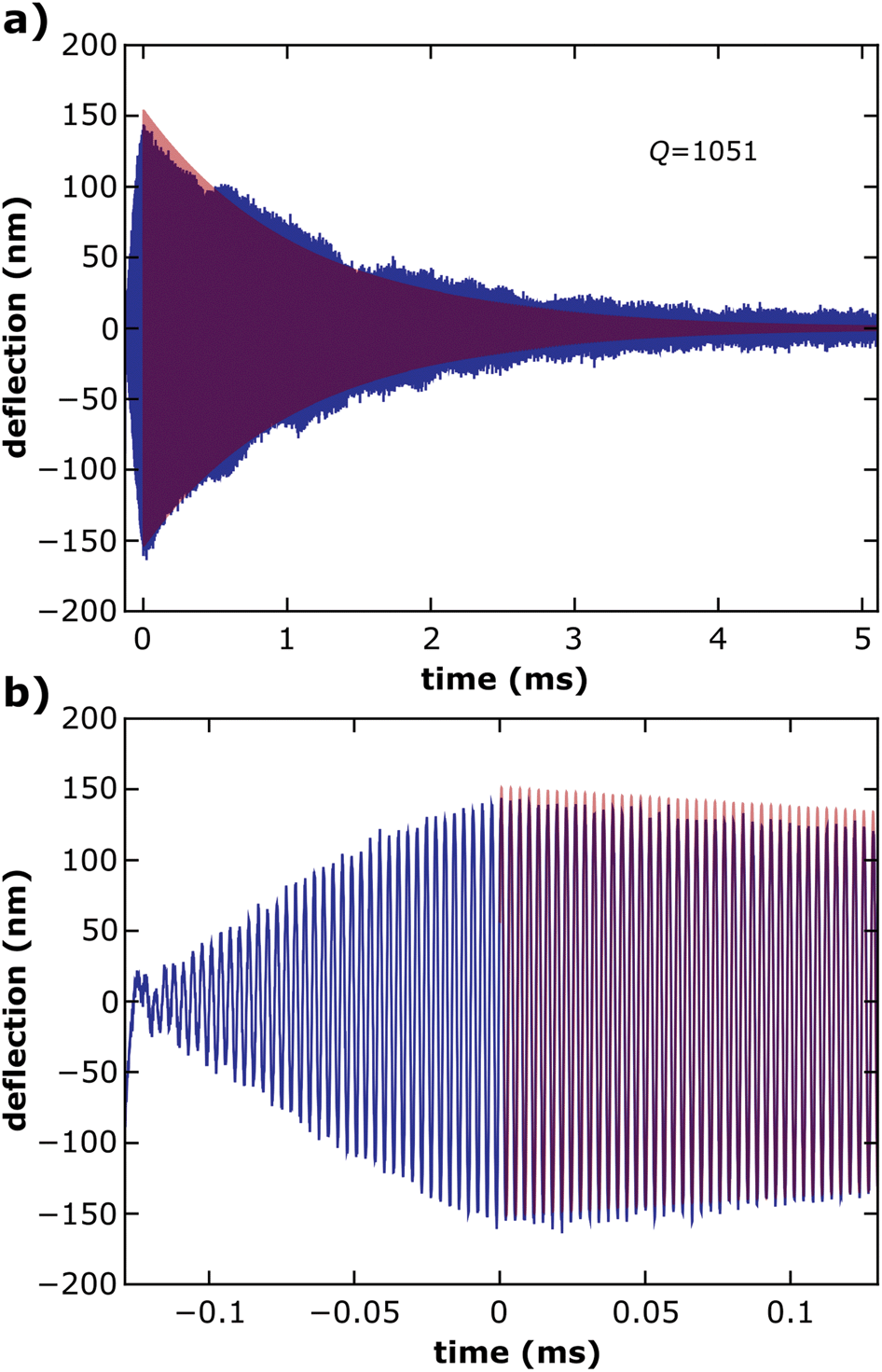 | ||
| Fig. 5 (a) Measured deflection time trace of a ring-down experiment for quality factor determination (blue). The GNP membrane was excited with 40 cycles of a sine voltage signal ending at t = 0 and the subsequent decay of the oscillation was recorded. The red line indicates a fit of the damped oscillator model (eqn (2)) to the deflection data. (b) The zoomed-in plot of the excitation interval and the beginning of the oscillation's decay. | ||
Conclusions
In summary, we reported the fabrication of electrostatically driven drumhead resonators based on freestanding membranes of organically cross-linked gold nanoparticles. The circular membranes with thicknesses of ∼34 nm or ∼51 nm and diameters of 100 μm or 50 μm showed fundamental resonance frequencies in the high kHz range and quality factors up to Q ∼ 2000 (see the ESI, Table S1†). In resonance, amplitudes of several hundreds of nanometers were measured under excitation with voltages below 30 V. The vibrational modes could be assigned unambiguously to the spectral positions of observed resonances by applying the theory for a clamped circular membrane with negligible bending stiffness.Currently, our investigations aim at the detailed understanding of the influences of membrane thickness, geometry and size on the resonators’ characteristics. Also the effects of external influences, such as pressure variations should be probed. Besides, the interplay of the internal structure of the membranes (cross-linker length, particle size) and their vibrational behavior (resonance frequencies, damping mechanisms) is an objective of our current research efforts. Higher resonance frequencies in the MHz range should be achievable by decreasing the lateral size of the freestanding membranes or their thicknesses. Furthermore, the potential applications of these resonators as pressure or gravimetric molecular sensors with electronic excitation and capacitive or resistive readout of the amplitude spectrum are topics for subsequent research activities.
Acknowledgements
The work of H. S. is supported by a scholarship from the Joachim Herz Stiftung. T. V. acknowledges financial support from the DFG, grant number VO698/3-1. We thank Dr Christian Strelow (University of Hamburg) and Dr Ralf Schüler (SIOS GmbH, Germany) for helpful discussions.References
- H. G. Craighead, Science, 2000, 290, 1532–1535 CrossRef CAS PubMed.
- D. R. Southworth, H. G. Craighead and J. M. Parpia, Appl. Phys. Lett., 2009, 94, 213506 CrossRef.
- M. Kumar and H. Bhaskaran, Nano Lett., 2015, 15, 2562–2567 CrossRef CAS PubMed.
- J. S. Bunch, A. M. van der Zande, S. S. Verbridge, I. W. Frank, D. M. Tanenbaum, J. M. Parpia, H. G. Craighead and P. L. McEuen, Science, 2007, 315, 490–493 CrossRef CAS PubMed.
- M. Tomi, A. Isacsson, M. Oksanen, D. Lyashenko, J.-P. Kaikkonen, S. Tervakangas, J. Kolehmainen and P. J. Hakonen, Nanoscale, 2015, 7, 14747–14751 RSC.
- Z. Wang, H. Jia, X. Zheng, R. Yang, Z. Wang, G. J. Ye, X. H. Chen, J. Shan and P. X.-L. Feng, Nanoscale, 2015, 7, 877–884 RSC.
- A. Castellanos-Gomez, R. van Leeuwen, M. Buscema, H. S. J. van der Zant, G. A. Steele and W. J. Venstra, Adv. Mater., 2013, 25, 6719–6723 CrossRef CAS PubMed.
- J. Lee, Z. Wang, K. He, J. Shan and P. X.-L. Feng, ACS Nano, 2013, 7, 6086–6091 CrossRef CAS PubMed.
- S. J. Cartamil-Bueno, P. G. Steeneken, F. D. Tichelaar, E. Navarro-Moratalla, W. J. Venstra, R. van Leeuwen, E. Coronado, H. S. J. van der Zant, G. A. Steele and A. Castellanos-Gomez, Nano Res., 2015, 8, 2842–2849 CrossRef CAS.
- X. Zhang, R. Waitz, F. Yang, C. Lutz, P. Angelova, A. Gölzhäuser and E. Scheer, Appl. Phys. Lett., 2015, 106, 063107 CrossRef.
- E. S. Park, Y. Chen, T.-J. K. Liu and V. Subramanian, Nano Lett., 2013, 13, 5355–5360 CrossRef CAS PubMed.
- S. Fuller, E. Wilhelm and J. Jacobson, J. Microelectromech. Syst., 2002, 11, 54–60 CrossRef.
- H. Schlicke, J. H. Schröder, M. Trebbin, A. Petrov, M. Ijeh, H. Weller and T. Vossmeyer, Nanotechnology, 2011, 22, 305303 CrossRef PubMed.
- B. Kowalczyk, M. M. Apodaca, H. Nakanishi, S. K. Smoukov and B. A. Grzybowski, Small, 2009, 5, 1970–1973 CrossRef CAS PubMed.
- S. Markutsya, C. Jiang, Y. Pikus and V. V. Tsukruk, Adv. Funct. Mater., 2005, 15, 771–780 CrossRef CAS.
- P. Kanjanaboos, X.-M. Lin, J. E. Sader, S. M. Rupich, H. M. Jaeger and J. R. Guest, Nano Lett., 2013, 13, 2158–2162 CrossRef CAS PubMed.
- F. J. Ibañez and F. P. Zamborini, Small, 2011, 8, 174–202 CrossRef PubMed.
- J. Herrmann, K. H. Müller, T. Reda, G. R. Baxter, B. Raguse, G. J. J. B. De Groot, R. Chai, M. Roberts and L. Wieczorek, Appl. Phys. Lett., 2007, 91, 183105 CrossRef.
- C. Farcau, H. Moreira, B. Viallet, J. Grisolia, D. Ciuculescu-Pradines, C. Amiens and L. Ressier, J. Phys. Chem. C, 2011, 115, 14494–14499 CAS.
- N. Olichwer, E. W. Leib, A. H. Halfar, A. Petrov and T. Vossmeyer, ACS Appl. Mater. Interfaces, 2012, 4, 6151–6161 CAS.
- C.-W. Jiang, I.-C. Ni, S.-D. Tzeng and W. Kuo, Sci. Rep., 2015, 5, 11939 CrossRef CAS PubMed.
- M. Brust, D. J. Schiffrin, D. Bethell and C. J. Kiely, Adv. Mater., 1995, 7, 795–797 CrossRef CAS.
- Y. Joseph, I. Besnard, M. Rosenberger, B. Guse, H.-G. Nothofer, J. M. Wessels, U. Wild, A. Knop-Gericke, D. Su, R. Schlögl, A. Yasuda and T. Vossmeyer, J. Phys. Chem. B, 2003, 107, 7406–7413 CrossRef CAS.
- H. Schlicke, E. W. Leib, A. Petrov, J. H. Schröder and T. Vossmeyer, J. Phys. Chem. C, 2014, 118, 4386–4395 CAS.
- H. Schlicke, M. Rebber, S. Kunze and T. Vossmeyer, Nanoscale, 2016, 8, 183–186 RSC.
- H. Schlicke, D. Battista, S. Kunze, C. J. Schröter, M. Eich and T. Vossmeyer, ACS Appl. Mater. Interfaces, 2015, 7, 15123–15128 CAS.
- D. V. Leff, L. Brandt and J. R. Heath, Langmuir, 1996, 12, 4723–4730 CrossRef CAS.
- V. P. Adiga, B. Ilic, R. a. Barton, I. Wilson-Rae, H. G. Craighead and J. M. Parpia, Appl. Phys. Lett., 2011, 99, 253103 CrossRef.
- Y. Joseph, N. Krasteva, I. Besnard, B. Guse, M. Rosenberger, U. Wild, A. Knop-Gericke, R. Schlögl, R. Krustev, A. Yasuda and T. Vossmeyer, Faraday Discuss., 2004, 125, 77–97 RSC.
Footnotes |
| † Electronic supplementary information (ESI) available. See DOI: 10.1039/C6NR02654K |
| ‡ These authors contributed equally to this work. |
| This journal is © The Royal Society of Chemistry 2016 |