
 Open Access Article
 This Open Access Article is licensed under a
 Creative Commons Attribution 3.0 Unported Licence
Phosphorene under electron beam: from monolayer to one-dimensional chains
Ville
Vierimaa
a,
Arkady V.
Krasheninnikov
bcde and
Hannu-Pekka
Komsa
*a
aCOMP, Department of Applied Physics, Aalto University, P.O. Box 1100, 00076 Aalto, Finland. E-mail: hannu-pekka.komsa@aalto.fi
bHelmholtz-Zentrum Dresden-Rossendorf, Institute of Ion Beam Physics and Materials Research, 01328 Dresden, Germany
cDepartment of Applied Physics, Aalto University, P.O. Box 1100, 00076 Aalto, Finland
dNational University of Science and Technology MISiS, 4 Leninskiy prospekt, Moscow, 119049, Russian Federation
eDepartment of Micro- and Nanotechnology (DTU Nanotech), Technical University of Denmark, Ørsteds Plads 345E, 2800 Kgs., Lyngby, Denmark
First published on 7th March 2016
Abstract
Phosphorene, a single sheet of black phosphorus, is an elemental two-dimensional material with unique properties and potential applications in semiconductor technology. While few-layer flakes of the material have been characterized using transmission electron microscopy, very little is known about its response to electron irradiation, which may be particularly important in the context of top-down engineering of phosphorus nanostructures using a focused electron beam. Here, using first-principles simulations, we study the production of defects in a single phosphorene sheet under impacts of energetic electrons. By employing the McKinley–Feshbach formalism and accounting for the thermal motion of atoms, we assess the cross section for atom displacement as a function of electron energy. We further investigate the energetics and dynamics of point defects and the stability of ribbons and edges under an electron beam. Finally, we show that P atomic chains should be surprisingly stable, and their atomic structure is not linear giving rise to the absence of a gap in the electronic spectrum.
1. Introduction
Exfoliation of graphene from a graphite crystal1 indicated that other two-dimensional (2D) systems can be manufactured, provided that the “parent” bulk material has a layered structure with the layers being bound together by weak van der Waals forces. Indeed, a large number of 2D materials such as hexagonal boron-nitride (h-BN),2 transition metal dichalcogenides (TMDs)3,4 and phosphorene5,6 have been produced from bulk counterparts by mechanical and liquid exfoliation techniques. The latter material derived from black phosphorus has recently attracted a lot of attention, as it is mechanically flexible,7 has high electron mobility8 and exhibits a gap of about 1–2 eV in the electronic spectrum, which is tunable by strain and the number of layers.9–112D materials have extensively been characterized by transmission electron microscopy (TEM), and their morphology (just a few layers of atoms) together with rapid progress in TEM and related spectroscopy methods made it possible to not only visualize directly the atomic structure, but also follow the motion of atoms and atomic structure transformations in real time with atomic resolution. Besides, beams of energetic electrons, which can nowadays be focused into a sub-Ångström area, have been shown to work as cutting and welding tools on the nanoscale.12 Specifically, nm-wide ribbons have been manufactured by the “top-down” approach, that is by electron-irradiation-induced sputtering of atoms, from sheets of graphene,13 h-BN,14 and TMDs.15–17 Moreover, as an ultimately narrow ribbon, free-standing atomic chains have been made starting from graphene13,18,19 and h-BN,14 which can serve as interconnects between 2D materials,20 along with beam-created nanowires in TMDs.16,17
Few-layer phosphorene sheets have been characterized by TEM.6,21–23 Electron-beam engineering of nanostructures based on a phosphorene sheet can be of particular interest, as defects in this system have been predicted to be electronically inactive,24 thus limiting the undesirable effects of unavoidable radiation damage of the system. Likewise, phosphorus chains, if stable, may exhibit intriguing electronic properties and unusual Peierls distortions due to fractional band filling. However, the efficient use of the electron beam for shaping and tuning phosphorene structures is virtually impossible without fundamental understanding of the response of this system to electron irradiation. At the same time, while the behavior of many other 2D materials – graphene,25–28 TMDs,29–31 and h-BN17,32–34 under electron beam has been studied at length, in phosphorene very little is known about the defect production mechanisms, defect dynamics, and irradiation damage development.
Here, using first-principles simulations, we study the production of defects in a single phosphorene sheet under electron beam. By employing the McKinley–Feshbach formalism and accounting for the thermal motion of atoms, we assess the cross section for atom displacement as a function of electron energy. We further investigate the energetics and dynamics of point defects and the stability of ribbons and edges under electron beam. Finally, we show that P atomic chains should be surprisingly stable, and their atomic structure is not linear giving rise to the absence of a gap in the electronic spectrum.
2. Methods
All simulations were based on density-functional theory (DFT) and carried out using the Vienna ab initio simulation package (VASP)35,36 with the PBE functional.37 The atomic structure of the pristine system was calculated using the plane-wave basis with a cut-off energy of 400 eV and a 12 × 12 k-point mesh.The knock-on radiation damage was assessed by calculating the displacement threshold energy Td, which corresponds to the minimum initial kinetic energy needed to displace a phosphorus atom from its original lattice site without its immediate recombination with the associated vacancy. Assuming an instantaneous momentum transfer from the impinging relativistic electron to the atom during the impact (it happens at the attosecond time scale38), an initial velocity was assigned to a selected P atom and the time evolution of the system was simulated using DFT molecular dynamics (MD). The initial kinetic energy was varied to trace the thresholds with an energy resolution of 0.5 eV. We used a time step of 0.5 fs, and a run time of 0.5–1 ps was usually sufficient to find out if the initial kinetic energy was high enough to produce a defect. The effect of spin-polarization (typically affecting the total energy by less than 0.1 eV) was found to have a negligible effect on the displacement thresholds at the adopted energy resolution, and thus calculations are carried out without spin-polarization. These calculations, as well as all calculations involving defects, were done using a 6 × 4 supercell. The Brillouin zone was sampled with a 2 × 3 Γ-centered k-point mesh.
Before knocking on another atom, the geometry of the structures with defects was fully optimized. At the same time, we calculated the formation energies of the produced defects:
| Ef = E(defect) − NPμP | (1) |
3. Results
3.1. Pristine systems
The atomic structures of several phosphorus-based systems are presented in Fig. 1. Fig. 1(a) shows the top and side views of the pristine phosphorene lattice, highlighting its puckered character. For the pristine system, we obtained lattice constants of a = 3.30 Å in the x-direction and b = 4.62 Å in the y-direction, in agreement with the values reported in the literature.7,41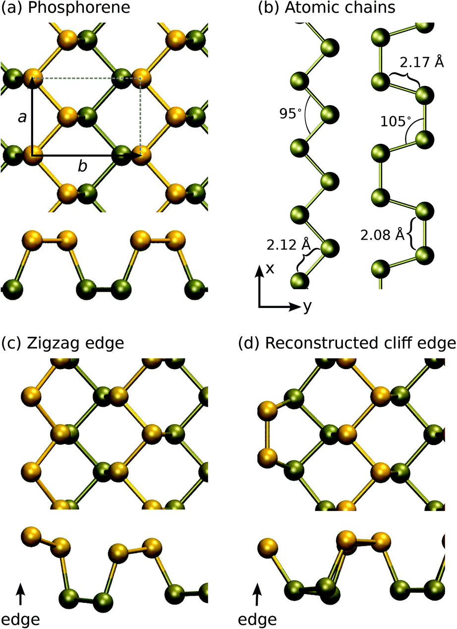 | ||
| Fig. 1 Atomic structures of (a) the pristine phosphorene, (b) atomic chains, (c) zigzag edge, and (d) reconstructed cliff edge. Selected structural parameters are listed. The atoms (and bonds) are colored according to their z-coordinates (perpendicular to the plane of the 2D material). | ||
For the edges in the zigzag direction, there are two inequivalent positions to cut the structure: in the middle of a terrace or in the middle of a cliff. Consequently, the system adopts two reconstructions, the zigzag (ZZ) and reconstructed cliff (RC), which, after structural relaxation become as shown in Fig. 1(c and d). The nanoribbon formation energy is defined as ENRf = E(ribbon) − NPμP, where E(ribbon) is the total energy of the ribbon composed of NP phosphorus atoms and μP is defined above. ENRf is plotted in Fig. 2 as a function of ribbon width for different types of the edges (two edges). Using the values for the widest ribbons considered, we obtain the edge energies of 0.70 eV and 0.52 eV per edge atom (or 0.21 eV Å−1 and 0.16 eV Å−1) for the ZZ and RC edges, respectively, in good agreement with those reported in ref. 42. Further information about the electronic, optical, and mechanical properties of phosphorene edges and wider nanoribbons can be found in ref. 43–47.
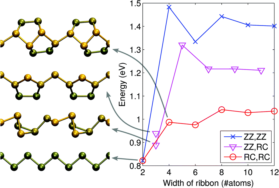 | ||
| Fig. 2 Formation energies of phosphorene nanoribbons with different combinations of edge reconstructions. The notations stand for the zigzag (ZZ) and reconstructed cliff (RC) edges. The atomic structures of the 2–4 atom wide systems are illustrated on the left. | ||
In the case of very thin ribbons, the system may relax strongly, which considerably lowers ENRf. The lowest energy structures are illustrated in Fig. 2. By running MD at 300 K, we ascertained that all the theoretical structures we found are at least metastable.
Ultimately, the thin ribbons turn into chains. The structures of pristine atomic chains were studied in more detail in linear, zigzag, and armchair configurations. The optimized structures for zigzag and armchair chains are shown in Fig. 1(b) and the structural parameters are listed in Table 1, along with cohesive energies. Moreover, phosphorus has a tendency to form P4-molecules, and although phosphorene is in the stable phase, both the bond length and cohesive energy of the P4 molecule and phosphorene are very similar.
| System | E coh (eV) | Bond length (Å) | Bond angle (°) |
|---|---|---|---|
| Phosphorene | 3.48 | 2.22, 2.26 | 96, 104 |
| P4 | 3.36 | 2.2 | 60 |
| Linear | 2.35 | 2.11 | 180 |
| Zigzag | 3.03 | 2.12 | 95 |
| Armchair | 2.93 | 2.08, 2.17 | 107 |
Calculations for chains showed that the linear configuration is unstable, and the system forms either a zigzag or an armchair structure, as shown in Fig. 1(b). The optimal configuration turned out to be a zigzag pattern, where the bond angle is 95° and bond length is 2.12 Å. The cohesive energy for zigzag chains is 3.03 eV, a value much larger than that for the simple linear chain. For the armchair pattern, there are two inequivalent bonds: the bond length between atoms in the direction of the chain (x-direction) is 2.08 Å, while in the transverse direction the length is 2.17 Å. The bond angle is 107° and the cohesive energy is 2.93 eV, slightly smaller than that for the zigzag chains. As compared to carbon chains,19 where the linear configuration is lower in energy because the sp1-hybridization naturally originates from the distribution of 4 electrons over the two sp1 and two transverse π-type bonds, the extra electron in phosphorus results in non-linear configurations.
3.2. Displacement threshold calculations
Having studied the atomic structure of phosphorene sheets, ribbons and chains, we move on to assess the radiation tolerance of these systems under electron beam using DFT MD. We stress that here we study only the knock-on damage. We will discuss other channels for defect production such as electronic excitation and electron-beam-induced chemical etching later on. As Td can be correlated with the formation energies of vacancy-type defects,29 we also studied the atomic structure and energetics of point defects. | ||
| Fig. 3 Atomic structures of (a) the pristine phosphorene, (b) Stone–Wales defect, (c) vacancy–adatom complex (VP − Pad), and (d) P adatom defect. The value in parentheses denotes the formation energy. The calculated displacement threshold energies (Ti) for selected atoms (Pi) are also shown and the resulting structures are indicated. | ||
Starting from pristine phosphorene, no damage is observed for T < Td ∼6 eV. When T ≥ 6 eV, the P1 atom has enough kinetic energy to break the bond to P2. The P3 atom then moves in to fill the vacant site. Finally, as P1 rebounds back to the original site, it forms a bond with P3 instead of P2. The final structure is shown in Fig. 3(b), and it effectively consists of a local bond rotation leading to 4-fold and 2-fold coordinated P atoms in contrast to the typical 3-fold coordination. In accordance with the bond rotation of carbon atoms in graphene, this defect was also named Stone–Wales defect (SW) in ref. 24. Larger kinetic energies lead to displacement of P1 to adatom sites or sputtering of P atoms.
From the SW defect the P1 atom can be displaced to a more distant adatom site with T ≥ 4.5 eV, where it may easily diffuse (see section 4), and finally [Fig. 3(d)] can be sputtered from the monolayer with T ≥ 4.5 eV. Thus, in order to start the process from pristine phosphorene, a minimum 6 eV kinetic energy is needed, but then irradiation would likely lead to sputtering of phosphorus atoms or possibly to formation of more complicated atomic structures.
Curiously, knock-on of the P2 atom from pristine phosphorene with T ≥ 7.5 eV leads to the formation of a vacancy–adatom complex (VP − Pad), which is shown Fig. 3(c). It is similar to the SW defect, but P1 is on a closeby adatom position and both P3 atoms around P1 have symmetrically moved in to bond with P2. Further knock-on events turn it into SW or lead to direct sputtering of the P1 atom, and thus does not change the general picture. Depending on the magnitude and direction of the collision, both of these should occur, but as evident from the formation energies shown in Fig. 3, the SW defect is clearly more stable. On a related note, we occasionally observed also other events. For instance, at T1 = 9.5 eV, P1 and P3 atoms swapped places (full bond rotation) and thus resulted in the pristine lattice. The T2 = 10 eV event first appeared to lead to the formation of the (VP − Pad) complex, but the P1 atom bounced back from the adatom site and the system returned to the pristine lattice.
The sputtering of phosphorus or displacing them to distant adatom sites leads to the formation of single vacancies. The P atoms next to the vacancy are likely less tightly bound than those in the pristine lattice and thus easier to displace. In order to manage the computational workload, we only calculated Td for selected atoms around the vacancy. Nevertheless, this is sufficient to obtain a general picture of how easily the vacancy may expand.
The results are shown in Fig. 4. A single vacancy with formation energy Ef = 1.67 eV is relatively unstable when compared to a double vacancy or larger vacancies, all having formation energies of about 0.7 eV per missing P atom. This is reflected also in the displacement thresholds. The P1 atom in VP is very easily displaced with T1 ≥ 3.5 eV, whereas the P2 atom in V2P requires T2 ≥ 6 eV and P3 atoms in V3P require T3 ≥ 5 eV.
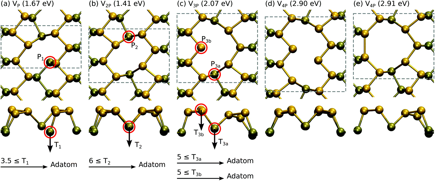 | ||
| Fig. 4 Atomic structures and formation energies for vacancies consisting of 1–4 missing P atoms. Displacement threshold energies are also given for selected atoms. | ||
Our formation energies are generally in agreement with those reported in previous studies,24,48 which can be referred to for discussion on the electronic structure of these defects. However, it is worth commenting on a few differences in our work. Our formation energy for V2P is in agreement with that in ref. 24, but is 0.5 eV lower than the rather similar-looking double vacancy in ref. 48. The slightly asymmetric structure given in ref. 48 can be obtained by displacing of one of the atoms next to the P2 atom to the bottom layer in Fig. 4(b). Hu and Yang also found another SW configuration that is 0.3 eV lower in energy than the one shown in Fig. 3(b), where the bond rotation involves P1 and P2 instead of P1 and P3. We did not observe this configuration in our molecular dynamics studies, but their formation is certainly possible. Nevertheless, this indicates that amorphization of phosphorene by bond rotations may be possible under electron irradiation similar to what is observed in graphene.49 Finally, we found that the Pad configuration shown in Fig. 3(d) on top of the bond-center is favored over the position reported in ref. 24. All of the above indicate that due to its flexibility phosphorene may possess large number of defect structures corresponding to local energy minima.
We found that similar to graphene,25 and unlike transition metal dichalcogenides,29 calculating unrelaxed vacancy formation energies does not give a good estimate for the displacement threshold, but requires explicit MD calculations of Td. Physically, this is the corollary of equal masses of all atoms in the system, which gives rise to the redistribution of the initial kinetic energy of the recoil atom: its neighbors “follow” it, as opposed to TMDs, where chalcogen atoms are considerably lighter than the neighboring transition metal atoms.
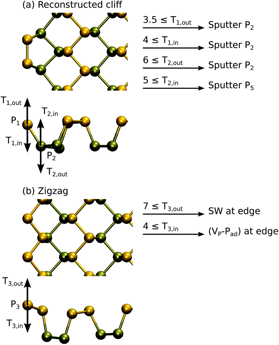
Here, we only determine the displacement thresholds, but do not attempt to trace further how the damage might progress. Although in practice the edge may be quite amorphous and expected to damage more quickly, our approach will still yield limits to the sputtering rate. In these calculations, to reduce the effects arising from the finite width of the ribbon, the non-damaged edge is passivated by hydrogen.9,43,45 The supercell is 6 units wide along the edge of the ribbon.
The results of DFT MD calculations are shown in Fig. 5. Starting from the case of the reconstructed cliff edge, which has lower edge energy, the outermost P atoms can be sputtered with energy of 3.5 eV or 4 eV, depending on the direction. For the second outermost row of P atoms, we found that Td is between 5 and 6 eV, very close to the values in the pristine sheet. The collisions mostly led to sputtering of P2 dimers from the edge, except for the T2,in case where a whole P5 ring was sputtered from the edge. Nevertheless, all cases resulted in formation of a zigzag edge. In the case of the zigzag edge, the outermost P atom can be displaced with an energy of 4 eV or 7 eV, depending on the direction, and usually instead of sputtering atoms this led to local reconstructions similar to those in the pristine systems. For three of the four cases involving outermost P atoms, Td is 3.5–4 eV and thus the edge should get easily destroyed. Only in the T3,out case the edge is expected to withstand radiation better and thus might be present more often during imaging.
 | ||
| Fig. 5 Atomic structures and calculated displacement threshold energies for the two reconstructions of the phosphorene zigzag edge. | ||
When the collision between an electron and the zigzag chain is simulated, there are three relevant non-equivalent cases to be considered: displacement of the two inequivalent atoms in the y-direction and displacement of one of the atoms in the z-direction [cf.Fig. 1(b)]. The simulations were made with two different supercells, the smaller one containing 12 atoms and the larger one 24 atoms. The smaller system was first used to find an estimate for threshold energy for chain breaking, but a larger supercell was needed to obtain quantitatively accurate results.
It turned out that when the initial velocity vector points away from the chain (the y-direction), the threshold energy is the highest, being around Td = 8 eV. A slightly surprising result is that the second y-direction and the z-direction have the same threshold energy of Td = 7 eV. At the threshold, the kinetic energy received by an atom is not enough to make it escape, but the chain will break into two parts. Below the threshold, the chains were strongly bent and the zigzag pattern became distorted. Nevertheless, the chains were able to stay intact for the whole simulation time of 900 fs. Moreover, one cannot exclude reconnection of the chains on a microscopic time-scale.
To gain further insight into stability of the chains, we also carried out molecular dynamics simulations at high temperatures. The initial configuration was chosen to be zigzag, as it has the lowest cohesive energy. The temperature in the simulations was kept constant using the Nose–Hoover thermostat. The time-step was chosen to be 1 fs.
Starting from T = 300 K, the system was simulated for a few picoseconds at time. If the chain was still intact, the temperature was increased and the simulation was continued from the final configuration of the previous simulation. The second simulation was done at T = 600 K and after that the temperature was increased by 200 K between simulations. The chains turned out to be surprisingly stable. As the temperature increases, the chains start to rotate around their axes while keeping the zigzag-pattern intact at temperatures up to 1400 K. After this, the chain breaks up into P2 and P4 molecules. The ability to rotate seems to be the main reason for the chains’ stability. It allows the atoms to have much more kinetic energy without escaping and breaking the chain. At temperatures of 600 K and above, the zigzag chains occasionally showed formation of armchair segments, but lasting for only a very short time. In simulations for the armchair chain, the system transformed back to the zigzag configuration within 1–2 ps, as expected on the basis of their cohesive energies (Table 1).
The effects of strain, which may be present and considerably affecting the electronic properties,50 were studied by elongating the unit cell in the x-direction. The percentage of elongation directly translates to strain and MD simulation allows us to find out the maximal amount the chain can sustain. The critical strain, after which the splitting happens, was estimated to be 13%. Also, a curious observation from the splitting is that the two atoms closest to the splitting point tend to rotate around the axis chains, terminating the chain ends with a P4-like configuration.
3.3. Cross sections
Using the values of displacement threshold energies calculated using DFT MD, we evaluated the cross sections for atom displacement. The knock-on damage cross sections were calculated at room temperature and are plotted in Fig. 6. The curve for Td = 6 eV represents the threshold for initiating damage in pristine phosphorene. An electron beam with 80 keV already has rather high cross section of 25 barns. Moreover, since the defects can grow rapidly, we conclude that 80 keV will likely quickly induce excessive damage. The energy of 60 keV should limit the damage of the pristine sheet, but will result in significant damage at the edges and defect sites. Note however that the divacancy (V2P, Td = 6 eV) should be stable under 60 keV. According to our calculations, most of the knock-on damage can be avoided when using a 30 keV electron beam. | ||
| Fig. 6 Calculated cross sections for knock-on damage induced by electron beam at selected displacement threshold energies and electron energies ranging from 0 to 300 kV. The shaded region indicates the variation in cross sections when moving from the static lattice to the Maxwell–Boltzmann velocity distribution at 300 K. | ||
We note that our calculations only yield a lower estimate for the knock-on displacement, but other processes such as electronic excitations, charging, and chemical reactions51,52 may also play a great role or even dominate. For instance, it was found that imaging at 15 kV or 30 kV leads to damaging of BN sheets, although their knock-on displacement thresholds are calculated to be clearly higher.14 However, charging and electronic excitation effects should be less important in phosphorene as it has a much smaller band gap, while etching contribution to the damage may be quite substantial due to high reactivity of phosphorene as evidenced e.g. by its strong propensity for oxidation.53,54
3.4. Defect dynamics
The molecular dynamics studies of knock-on events also hinted of efficient dynamics of defects, which include their migration and transformations between different types of defects. We first consider the barriers for the transformations between defect configurations that conserve the total number of atoms in the system, i.e., the Stone–Wales and the (VP − Pad) defects. The energetics of the transformation with respect to pristine phosphorene is shown in Fig. 7. Formation of SW defects requires overcoming a barrier of 2.30 eV. This value is rather low, at least when compared to graphene,25 indicating that the defects can be formed at high temperatures. On the other hand, healing of the SW defect only requires 0.81 eV and thus even if they are plentiful after e.g. irradiation experiments, they can also be quickly removed. The barriers between (VP − Pad) and SW are small, but since SW is lower in energy, it is expected to be predominantly present.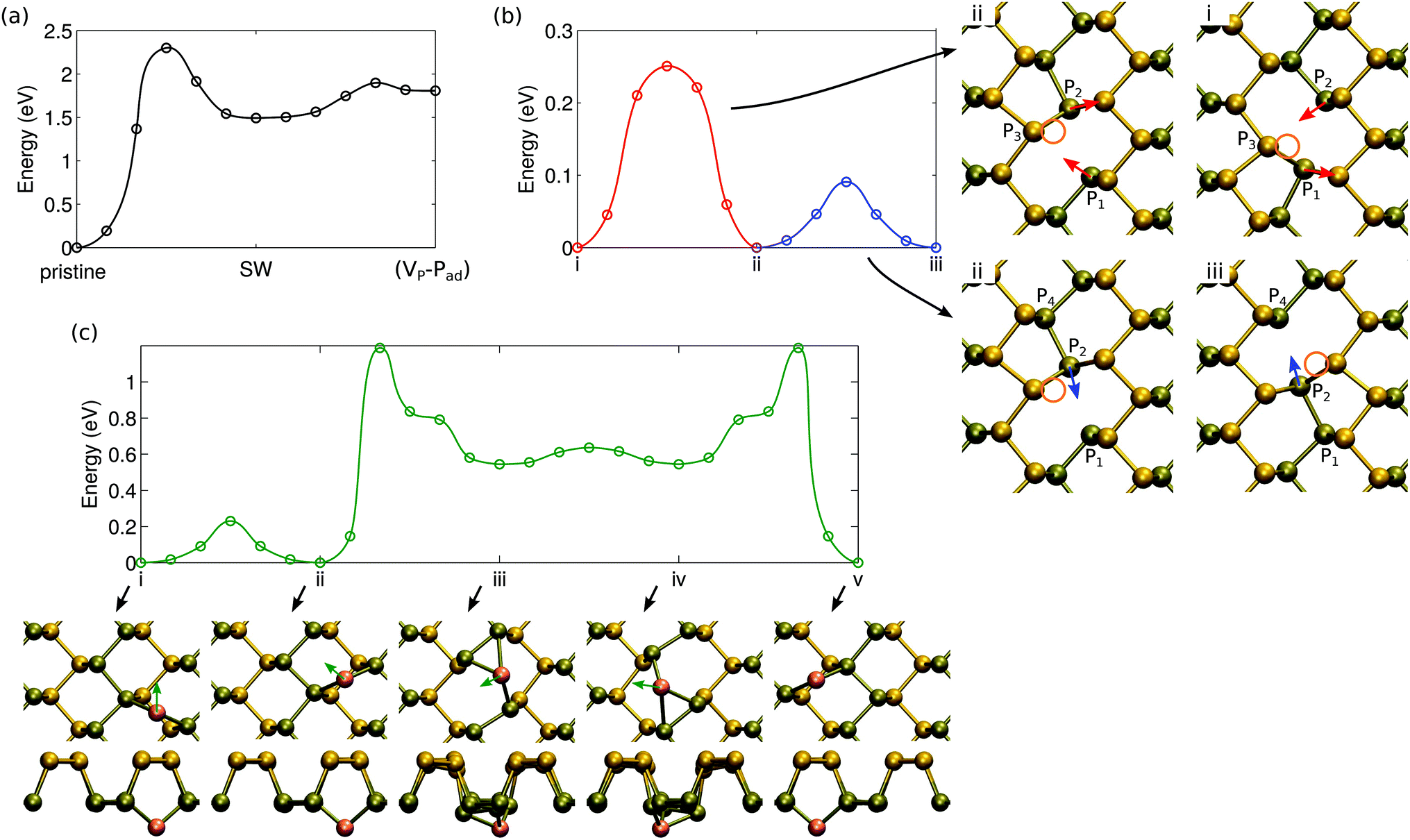 | ||
| Fig. 7 Migration barriers and the corresponding atomic structures for (a) formation of atom number conserving defects, (b) single vacancy diffusion along the trench, and (c) adatom diffusion along and over the trench. In (b), the two rebonding mechanisms are illustrated by arrows (red and blue) and vacancies by circles (orange) in the atomic structures. In (c), the adatom is highlighted with orange color and movement with arrows (green). | ||
Clustering of vacancies will be limited by the rate of vacancy diffusion. Diffusion of a single vacancy consists of two separate steps, which do not involve a clear jump of atoms from one site to another, but rather involve changes in the local bonding, similar to vacancy diffusion in carbon nanotubes.55 As illustrated by configurations i and ii in Fig. 7(b), there can be a switch in the bonding between the two Jahn–Teller symmetry broken structures, which only involves movement of atoms P1 and P2 w.r.t. atom P3. The P vacancy remains next to atom P3. The energy barrier for this process is 0.25 eV. In addition, as illustrated by configurations ii and iii, atom P2 can easily switch bonding to either atom P1 or atom P4 with only a very small change in its position. Consequently, the vacancy has moved to the neighboring lattice site. The small change in the geometry is reflected in a very small migration barrier, only 0.09 eV. Either of these barriers is low enough to warrant that rapid diffusion should occur even at room temperature.
In the case of adatoms, diffusion along the trench, from one “bond-center” site to another (from i to ii), is easy, with a barrier of only 0.23 eV. The path for migrating from one trench to another is more complicated as shown in Fig. 7(c) (configurations ii to v). The rate is limited by the barrier of 1.19 eV – this energy is required to move from the trench to the middle of the ridge.
3.5. Electronic structure of phosphorus chains
The band structure and the density of states for the zigzag chain are shown in Fig. 8. In addition to the total density of states, projected densities of states (PDOS) are also calculated to gain insight into the electronic structure. PDOS allows us to immediately recognize some of the bands to be formed by certain orbitals. The yellow-coloured bands are largely formed out of pz-orbitals forming π-bonds.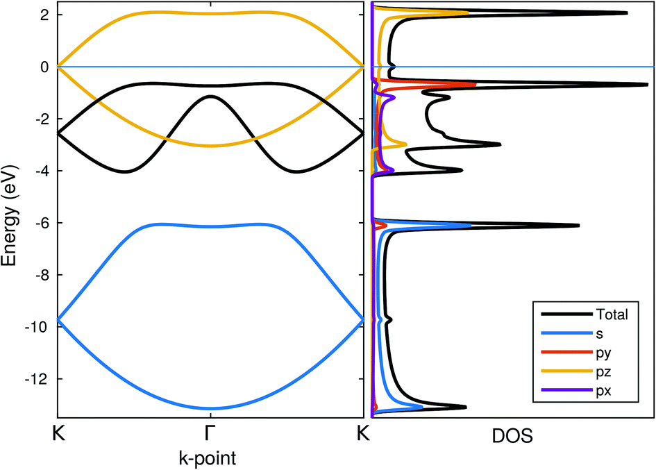 | ||
| Fig. 8 Band structure, total density of states and orbital-projected density of states for zigzag chains. Energy zero is set at the Fermi-level. | ||
The blue-coloured bands originate mostly from s-orbitals with a small px/py contribution and the black bands from px/py-orbitals with a small contribution from s. These bands are associated with the P–P bonds in the chain: the bonds lie in the xy-plane but they are not aligned with either of the major axis and therefore appear in both of the projections. Thus, they can both be considered as σ-bonds, the former arising from s-orbitals and the latter from px/py-orbitals. The minor mixing of the orbital characters indicates partial sp2-hybridization, which is also evidenced in the 95° angle found in the zigzag chain.
The system always remained (semi-)metallic with a half-filled π-band and the Fermi-level crossing it at the K-point. No indication for the Peierls-type transition was found apparently due to a non-linear structure of the chain.
4. Conclusions
Defect production in single phosphorene sheet under impacts of energetic electrons was studied using first principles calculations. Molecular dynamics was used to gain insights into time evolution of the system after impacts from electrons and the displacement cross sections were determined through the McKinley–Feshbach formalism. Although we focused on the stability under electron beam, the calculated displacement threshold energies, the most important quantities in radiation physics, are equally valid for ion or neutron irradiation, and the amount of damage in each case can be estimated using the Kinchin–Pease model.56In pristine phosphorene, the damage is expected to begin from the formation of Stone–Wales defects, from which P atoms can then be relatively easily displaced, finally leading to vacancy formation. The calculated displacement threshold is low enough that a 80 keV beam should rapidly lead to a considerable amount of damage. With 60 keV electrons, the initial SW production can be avoided. Next, we considered defect dynamics and stability of edges under electron beam. To avoid sputtering of P atoms from defect sites or from edges, the beam energy should preferably be even less than 60 keV. We stress that the knock-on damage mechanism should dominate under ultra-high vacuum conditions to prevent oxidation of phosphorus nanostructures and the associated etching. Phosphorene sheets may be encapsulated between graphene sheets, though, which should protect them from the interaction with the environment, similar to TMDs.31,57,58
Finally, upon continuing thinning of nanoribbons by the electron beam, P atomic chains are expected to form. Calculations indicated them to be surprisingly stable, both thermally and under electron beam. They adopt zigzag configuration and their atomic structure is not linear giving rise to the absence of a gap in the electronic spectrum.
Acknowledgements
The work was carried out with partial financial support from the Academy of Finland through Projects no. 263416 and 286279. HPK and VV further thank the Academy of Finland for the support through its Centres of Excellence Programme (2012–2017) under the Project No. 251748. AVK also acknowledges the financial support of the Ministry of Education and Science of the Russian Federation in the framework of Increase Competitiveness Program of NUST “MISiS” (#K2-2015-033). We also thank the CSC-IT Center for Science Ltd and the Aalto Science-IT project for generous grants of computer time.References
- K. S. Novoselov, A. K. Geim, S. V. Morozov, D. Jiang, Y. Zhang, S. V. Dubonos, I. V. Grigorieva and A. A. Firsov, Science, 2004, 306, 666–669 CrossRef CAS PubMed.
- D. Golberg, Y. Bando, Y. Huang, T. Terao, M. Mitome, C. Tang and C. Zhi, ACS Nano, 2010, 4, 2979–2993 CrossRef CAS PubMed.
- M. Chhowalla, H. S. Shin, G. Eda, L.-j. Li, K. P. Loh and H. Zhang, Nat. Chem., 2013, 5, 263–275 CrossRef PubMed.
- Q. H. Wang, K. Kalantar-Zadeh, A. Kis, J. N. Coleman and M. S. Strano, Nat. Nanotechnol., 2012, 7, 699–712 CrossRef CAS PubMed.
- W. Lu, H. Nan, J. Hong, Y. Chen, C. Zhu, Z. Liang, X. Ma, Z. Ni, C. Jin and Z. Zhang, Nano Res., 2014, 7, 853–859 CrossRef CAS.
- J. R. Brent, N. Savjani, E. A. Lewis, S. J. Haigh, D. J. Lewis and P. O'Brien, Chem. Commun., 2014, 50, 13338–13341 RSC.
- Q. Wei and X. Peng, Appl. Phys. Lett., 2014, 104, 251915 CrossRef.
- H. Liu, A. T. Neal, Z. Zhu, Z. Luo, X. Xu, D. Tománek and P. D. Ye, ACS Nano, 2014, 8, 4033–4041 CrossRef CAS PubMed.
- L. Liang, J. Wang, W. Lin, B. G. Sumpter, V. Meunier and M. Pan, Nano Lett., 2014, 14, 6400–6406 CrossRef CAS PubMed.
- X. Peng, Q. Wei and A. Copple, Phys. Rev. B: Condens. Matter, 2014, 90, 085402 CrossRef.
- V. Tran, R. Soklaski, Y. Liang and L. Yang, Phys. Rev. B: Condens. Matter, 2014, 89, 235319 CrossRef.
- A. V. Krasheninnikov and F. Banhart, Nat. Mater., 2007, 6, 723–733 CrossRef CAS PubMed.
- C. Jin, H. Lan, L. Peng, K. Suenaga and S. Iijima, Phys. Rev. Lett., 2009, 102, 205501 CrossRef PubMed.
- O. Cretu, H.-P. Komsa, O. Lehtinen, G. Algara-Siller, U. Kaiser, K. Suenaga and A. V. Krasheninnikov, ACS Nano, 2014, 8, 11950–11957 CrossRef CAS PubMed.
- X. Liu, T. Xu, X. Wu, Z. Zhang, J. Yu, H. Qiu, J.-H. Hong, C.-H. Jin, J.-X. Li, X.-R. Wang, L.-T. Sun and W. Guo, Nat. Commun., 2013, 4, 1776 CrossRef PubMed.
- O. Lehtinen, H.-p. Komsa, A. Pulkin, M. B. Whitwick, M.-w. Chen, T. Lehnert, M. J. Mohn, O. V. Yazyev, A. Kis, U. Kaiser and A. V. Krasheninnikov, ACS Nano, 2015, 9, 3274–3283 CrossRef CAS PubMed.
- J. Lin, O. Cretu, W. Zhou, K. Suenaga, D. Prasai, K. I. Bolotin, N. T. Cuong, M. Otani, S. Okada, A. R. Lupini, J.-C. Idrobo, D. Caudel, A. Burger, N. J. Ghimire, J. Yan, D. G. Mandrus, S. Pennycook and S. Pantelides, Nat. Nanotechnol., 2014, 9, 436–442 CrossRef CAS PubMed.
- A. Chuvilin, J. C. Meyer, G. Algara-Siller and U. Kaiser, New J. Phys., 2009, 11, 083019 CrossRef.
- O. Cretu, A. R. Botello-Mendez, I. Janowska, C. Pham-Huu, J.-C. Charlier and F. Banhart, Nano Lett., 2013, 13, 3487–3493 CrossRef CAS PubMed.
- Y. Rong and J. H. Warner, ACS Nano, 2014, 8, 11907–11912 CrossRef CAS PubMed.
- J. Sun, H.-w. Lee, M. Pasta, H. Yuan, G. Zheng, Y. Sun, Y. Li and Y. Cui, Nat. Nanotechnol., 2015, 10, 980–985 CrossRef CAS PubMed.
- A. Bachmatiuk, J. Zhao, S. M. Gorantla, I. G. G. Martinez, J. Wiedermann, C. Lee, J. Eckert and M. H. Rummeli, Small, 2015, 11, 515–542 CrossRef CAS PubMed.
- A. Castellanos-Gomez, L. Vicarelli, E. Prada, J. O. Island, K. L. Narasimha-Acharya, S. I. Blanter, D. J. Groenendijk, M. Buscema, G. A. Steele, J. V. Alvarez, H. W. Zandbergen, J. J. Palacios and H. S. J. van der Zant, 2D Materials, 2014, 1, 025001 CrossRef.
- Y. Liu, F. Xu, Z. Zhang, E. S. Penev and B. I. Yakobson, Nano Lett., 2014, 14, 6782–6786 CrossRef CAS PubMed.
- F. Banhart, J. Kotakoski and A. V. Krasheninnikov, ACS Nano, 2011, 5, 26–41 CrossRef CAS PubMed.
- J. C. Meyer, F. Eder, S. Kurasch, V. Skakalova, J. Kotakoski, H. J. Park, S. Roth, A. Chuvilin, S. Eyhusen, G. Benner, A. V. Krasheninnikov and U. Kaiser, Phys. Rev. Lett., 2012, 108, 196102 CrossRef PubMed.
- A. W. Robertson, G.-D. Lee, K. He, E. Yoon, A. I. Kirkland and J. H. Warner, Nano Lett., 2014, 14, 1634–1642 CrossRef CAS PubMed.
- R. Zan, Q. Ramasse, U. Bangert and K. S. Novoselov, Nano Lett., 2012, 12, 3936–3940 CrossRef CAS PubMed.
- H.-P. Komsa, J. Kotakoski, S. Kurasch, O. Lehtinen, U. Kaiser and A. V. Krasheninnikov, Phys. Rev. Lett., 2012, 109, 035503 CrossRef PubMed.
- H.-P. Komsa, S. Kurasch, O. Lehtinen, U. Kaiser and A. V. Krasheninnikov, Phys. Rev. B: Condens. Matter, 2013, 88, 035301 CrossRef.
- R. Zan, Q. Ramasse, R. Jalil, T. Georgiou, U. Bangert and K. S. Novoselov, ACS Nano, 2013, 7, 10167–10174 CrossRef CAS PubMed.
- C. Jin, F. Lin, K. Suenaga and S. Iijima, Phys. Rev. Lett., 2009, 102, 195505 CrossRef PubMed.
- A. Pakdel, Y. Bando and D. Golberg, Chem. Soc. Rev., 2014, 43, 934–959 RSC.
- N. Alem, Q. Ramasse, C. R. Seabourne, O. Yazyev, K. Erickson, M. C. Sarahan, C. Kisielowski, A. J. Scott, S. Louie and A. Zettl, Phys. Rev. Lett., 2012, 109, 205502 CrossRef PubMed.
- G. Kresse and J. Hafner, Phys. Rev. B: Condens. Matter, 1993, 47, 558–561 CrossRef CAS.
- G. Kresse and J. Furthmüller, Comput. Mater. Sci., 1996, 6, 15–50 CrossRef CAS.
- J. P. Perdew, K. Burke and M. Ernzerhof, Phys. Rev. Lett., 1996, 77, 3865 CrossRef CAS PubMed.
- F. Banhart, Rep. Prog. Phys., 1999, 62, 1181 CrossRef CAS.
- G. Henkelman, B. P. Uberuaga and H. Jónsson, J. Chem. Phys., 2000, 113, 9901–9904 CrossRef CAS.
- W. A. McKinley and H. Feshbach, Phys. Rev., 1948, 74, 1759–1763 CrossRef CAS.
- L. C. L. Y. Voon, A. Lopez-Bezanilla, J. Wang, Y. Zhang and M. Willatzen, New J. Phys., 2015, 17, 025004 CrossRef.
- A. Ramasubramaniam and A. R. Muniz, Phys. Rev. B: Condens. Matter, 2014, 90, 085424 CrossRef.
- A. Carvalho, A. S. Rodin and A. H. C. Neto, Europhys. Lett., 2014, 108, 47005 CrossRef.
- V. Tran and L. Yang, Phys. Rev. B: Condens. Matter, 2014, 89, 245407 CrossRef.
- W. Li, G. Zhang and Y.-W. Zhang, J. Phys. Chem. C, 2014, 118, 22368–22372 CAS.
- V. Sorkin and Y. W. Zhang, Nanotechnology, 2015, 26, 235707 CrossRef CAS PubMed.
- Y. Du, H. Liu, B. Xu, L. Sheng, J. Yin, C.-G. Duan and X. Wan, Sci. Rep., 2015, 5, 8921 CrossRef CAS PubMed.
- W. Hu and J. Yang, J. Phys. Chem. C, 2015, 119, 20474–20480 CAS.
- J. Kotakoski, A. V. Krasheninnikov, U. Kaiser and J. C. Meyer, Phys. Rev. Lett., 2011, 106, 105505 CrossRef CAS PubMed.
- A. La Torre, A. Botello-Mendez, W. Baaziz, J. C. Charlier and F. Banhart, Nat. Commun., 2015, 6, 6636 CrossRef CAS PubMed.
- J. Cazaux, Ultramicroscopy, 1995, 60, 411–425 CrossRef CAS.
- R. F. Egerton, P. Li and M. Malac, Micron, 2004, 35, 399–409 CrossRef CAS PubMed.
- S. P. Koenig, R. A. Doganov, H. Schmidt, A. H. Castro Neto and B. Özyilmaz, Appl. Phys. Lett., 2014, 104, 103106 CrossRef.
- A. Ziletti, A. Carvalho, D. K. Campbell, D. F. Coker and A. H. Castro Neto, Phys. Rev. Lett., 2015, 114, 046801 CrossRef CAS PubMed.
- A. V. Krasheninnikov, P. O. Lehtinen, A. S. Foster and R. M. Nieminen, Chem. Phys. Lett., 2006, 418, 132–136 CrossRef CAS.
- G. H. Kinchin and R. S. Pease, Rep. Prog. Phys., 1955, 18, 1 Search PubMed.
- G. Algara-Siller, S. Kurasch, M. Sedighi, O. Lehtinen and U. Kaiser, Appl. Phys. Lett., 2013, 103, 203107 CrossRef.
- Y. Cao, A. Mishchenko, G. L. Yu, E. Khestanova, A. P. Rooney, E. Prestat, A. V. Kretinin, P. Blake, M. B. Shalom, C. Woods, J. Chapman, G. Balakrishnan, I. V. Grigorieva, K. S. Novoselov, B. A. Piot, M. Potemski, K. Watanabe, T. Taniguchi, S. J. Haigh, A. K. Geim and R. V. Gorbachev, Nano Lett., 2015, 15, 4914–4921 CrossRef CAS PubMed.
| This journal is © The Royal Society of Chemistry 2016 |