
Rapid fabrication of ZnO nanorod arrays with controlled spacing by micelle-templated solvothermal growth†
Candice I.
Pelligra
,
Kristof
Toth
,
Hanqiong
Hu
and
Chinedum O.
Osuji
*
Department of Chemical and Environmental Engineering, Yale University, New Haven, CT 06511, USA. E-mail: chinedum.osuji@yale.edu
First published on 23rd November 2015
Abstract
We present a facile method for the synthesis of nanorod arrays over large areas with fine control over the average rod–rod spacing. Block copolymer micelles are used to template solvothermal synthesis of ZnO nanorods by preferentially enabling reactant diffusion through the micelle cores to an underlying seed layer. The distance between nanorod centers is defined by the micelle number density which is in turn controlled by the molecular weight of the block copolymer, and the block copolymer concentration in a templating film. We demonstrate the ability to control the resulting nanorod number density from ∼100 μm−2 down to ∼10 μm−2 with high fidelity. Correspondingly, the distance between nanorod surfaces was varied from ∼60 nm to 230 nm. The method developed here provides a viable approach for rapidly fabricating large-area nanostructured electrodes comprised of nanorod arrays with controlled geometries. The ability to tailor nanorod spacing over a broad range suggests applications in photovoltaics and sensors based on optical resonances can be readily addressed.
Nanostructured electrodes can offer compelling advantages in thin film devices, relative to their non-structured or flat counterparts. In the context of photovoltaics, a particular focus has developed around electrodes or active layers employing vertically aligned nanorods with geometries that are engineered to match the electro-optic and transport properties of the materials in the active layer of the device. Such nanorod structures may permit tuning of optical field intensity within the active layer,1,2 provide increased surface area for exciton dissociation,3,4 and serve to efficiently collect and shuttle charge through an otherwise relatively low mobility active layer material.5–8 Recent work on PbS quantum dot infiltrated ZnO nanorod arrays9 in an ordered bulk heterojunction motif highlights the importance of rationally engineering the nanorod spacing for such devices. For polymer-based systems, the charge transport-limiting length scale is ∼10 nm and therefore the optimal nanorod surface-to-surface separation is ∼20 nm. In quantum dot-based devices the relevant length scale is roughly an order of magnitude larger. The ability to tune nanorod spacing based on characteristic transport lengths for different active layer materials is critical for device optimization. The lack of scalable approaches for achieving such optimization represents a critical hurdle in device development.
Solvothermal synthesis using seeded substrates has emerged as an attractive method for low-cost and large-area preparation of metal oxide nanorods such as ZnO and TiO2, often cited for use in photovoltaics. Unconstrained solvothermal growth typically leads to the formation of tightly packed nanorods.10,11 Such dense nanorod forests, as they are called, represent a sub-optimal solution. Efforts have been made to control the density of nanorods produced in solvothermal synthesis. Empirical approaches include adjusting process parameters in seed layer preparation,12–14 modifying reactant concentrations,12,15 kinetically hindering growth using barrier films,16 and even eliminating the seeding step altogether.17 Nevertheless, it remains difficult to reliably control the resulting nanorod density. More importantly perhaps, the aforementioned approaches are empirical and therefore do not provide rational control of nanorod density.
Templated synthesis differs strongly in this respect as it allows in principle a priori specification, and therefore rational control, of the density of the resulting nanorod array. Rapid epitaxial growth of single crystals of ZnO has been achieved through resist templates patterned by soft nanoimprint lithography and low temperature aqueous growth.18,19 Additional efforts have primarily employed block copolymer micelles to sequester Zn-species. The micelles are processed by heat or plasma treatment to create ZnO nanoparticles which seed nanorod growth in a subsequent vapor-phase process.20–23 More recently, direct templating of hydrothermal growth of ZnO nanorod arrays from uniform seed layers through poly(styrene)-b-poly(4-vinyl pyridine) (PS-b-P4VP) micelle cores as developed by the present authors,24 and etched ordered block copolymer (BCP) thin films,25 have been demonstrated. The method introduced by our group provides the ability to create nanorod arrays with densities dictated by the number density of micelles in the monolayer film used as the template for nanorod growth. The micelle number density, ν, is a strict function of the molecular weight, M, of the block copolymer, with ν ∼ M−2α where α, typically ranging from 1/2 to 2/3, relates the radius of gyration of the polymer to its molecular weight, Rg ∼ Mα. Using a reasonably high molecular weight system, P4VP with molecular weight Mn = 258 kDa and PS weight fraction fPS = 0.91 (PS-b-P4VP 235/23 K) we were able to fabricate nanorod arrays as sparse as ∼100 μm−2, matching the number density of micelles in the monolayer template within 15%. The use of lower molecular weight block copolymers (22 K) permitted access to nanorod densities as high as 1250 μm−2. However, the ability to fabricate array densities well below 100 μm−2 is severely constrained by the challenges, from a process perspective, of synthesizing and working with block copolymers with the inordinately high molecular weights that would be required. At the same time there is a firm need to extend the range of accessible densities below 100 μm−2 to address compelling possibilities in quantum-dot based photovoltaics9,26,27 and sensors based on optical resonances within nanorod arrays28–30 wherein many other methods of templating, often requiring expensive processing or specialized substrates, have proven insufficient. Further, there is a need to explore the use of alternate chemistries for the template layer, to enable access to syntheses at different (higher) temperatures than previously possible.
Here we demonstrate a simple method for fabricating nanorod arrays with densities below 100 μm−2. The approach is based on the use of a homopolymer (HP) additive to reduce the number density of micelles in the templating monolayer where the HP is chemically identical to the corona of the BCP micelles. The method allows access to arbitrarily small nanorod densities. We show here ZnO nanorod arrays with densities down to 10 μm−2. We also demonstrate array fabrication using a second BCP which allows the use of significantly higher reaction temperatures than PS-b-P4VP. This system extends the range of solvothermal nanomaterial syntheses which can be templated using the BCP micelle-based approach.
The fabrication concept is schematically represented in Fig. 1. Micelles are distributed with the homopolymer in a confluent film atop a ZnO seed layer. Diffusion of the reactants from the aqueous media through the water-insoluble PS homopolymer and corona chains is aided by the presence of a water-miscible swelling agent, acetone, in the growth solution. The high affinity of pyridine for Zn2+ and the polar nature of P4VP facilitate comparatively rapid transport of the reactants through the micelle cores to the seed layer which enables the subsequent growth of nanorods up through the cores. The average distance s between nanorod surfaces is given in eqn (1) (see ESI† for derivation). It is a simple function of the micelle core diameter, dc, the nanorod diameter, dnr, the volume fraction of the core block, ϕc, and the dimensionless concentration of the BCP in the film, CBCP. Note that the micelle core diameter is related to the overall micelle diameter by the core volume fraction, dc = ϕcdm. The dimensionless concentration CBCP = 1 for a film composed only of the BCP, and decreases as the presence of homopolymer dilutes the micelles in the film.
 | (1) |
 | ||
| Fig. 1 Concept for hydrothermal growth through homopolymer-diluted micelle templates. (a) Close-packed micelle monolayer, (b) homopolymer blended into BCP-solution separates micelles in the spincast micelle monolayer with a spacing proportional to the ratio of weight fraction relative to BCP, (c) ZnO nanorods grow selectively through micelle cores after swelling with solvent additive and hydrothermal growth. | ||
PS-b-P4VP diblock copolymer (Mn, PS/Mn, P4VP = 235 kDa/23 kDa) from Polymer Source, Inc. (PDI = 1.1–1.2) was dissolved in toluene with PS homopolymer (Scientific Polymer Products) (210 kDa) to form 0.5 wt% solutions with varying BCP content defined by the mass ratio of HP![[thin space (1/6-em)]](https://www.rsc.org/images/entities/char_2009.gif) :BCP present. The solutions were stirred for 5–7 hours at room temperature and then left overnight (8–10 hours) in an oven at 70–80 °C to decrease polydispersity in the size and shape of the micelles. The BCP–HP solutions were spin-cast at 2k rpm onto a ZnO seed layer on silicon prepared according to previously established methods.31 The BCP–HP forms a confluent homopolymer-diluted micelle monolayer as shown in Fig. 1b. Micelle monolayer-coated seeded substrates were inserted into vials of aqueous ZnO growth solution consisting of 0.0125 M zinc acetate dihydrate (Sigma-Aldrich, >98%) and 0.0250 M hexamethylenetetramine (Sigma-Aldrich, >99%) dissolved in deionized (DI) water with 5 vol% of acetone added. The substrates were held in an inverted position in the growth solution to prevent sedimentation of precipitates from the solution which could interfere with the nanorod growth. The vials were closed tightly and submerged in a water bath held at 70 °C. The reaction was allowed to proceed for 15–45 minutes depending on desired nanorod length. Nanorods much longer than shown here should be accessible by suitable tuning of the reaction time and conditions. Upon removal from the growth solution, the resulting arrays are rinsed of any residue, slowly dried, and treated with oxygen plasma for several minutes (typically ∼5–10 minutes) to remove any residual polymer template which is not delaminated during the hydrothermal growth process.
:BCP present. The solutions were stirred for 5–7 hours at room temperature and then left overnight (8–10 hours) in an oven at 70–80 °C to decrease polydispersity in the size and shape of the micelles. The BCP–HP solutions were spin-cast at 2k rpm onto a ZnO seed layer on silicon prepared according to previously established methods.31 The BCP–HP forms a confluent homopolymer-diluted micelle monolayer as shown in Fig. 1b. Micelle monolayer-coated seeded substrates were inserted into vials of aqueous ZnO growth solution consisting of 0.0125 M zinc acetate dihydrate (Sigma-Aldrich, >98%) and 0.0250 M hexamethylenetetramine (Sigma-Aldrich, >99%) dissolved in deionized (DI) water with 5 vol% of acetone added. The substrates were held in an inverted position in the growth solution to prevent sedimentation of precipitates from the solution which could interfere with the nanorod growth. The vials were closed tightly and submerged in a water bath held at 70 °C. The reaction was allowed to proceed for 15–45 minutes depending on desired nanorod length. Nanorods much longer than shown here should be accessible by suitable tuning of the reaction time and conditions. Upon removal from the growth solution, the resulting arrays are rinsed of any residue, slowly dried, and treated with oxygen plasma for several minutes (typically ∼5–10 minutes) to remove any residual polymer template which is not delaminated during the hydrothermal growth process.
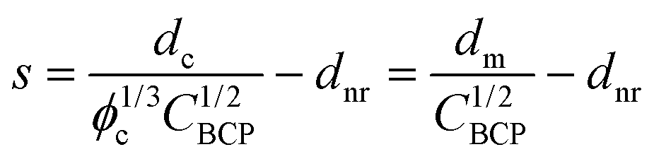
Atomic force microscopy (AFM) images of diluted PS-b-P4VP micelle monolayers alongside images of the corresponding neat (non-diluted) PS-b-P4VP monolayer are shown in Fig. 2 for 235/23 K diluted to mass fractions 4:1 and 9:1 of HP:BCP. An additional 2:1 dilution is shown in ESI Fig. S1.† The low level of phase contrast is consistent with the expectation that the lower surface tension PS chains would be present at the air interface and the P4VP cores would be located preferentially at the substrate. Height measurements show that the film roughness is significantly smaller than the lateral micelle dimensions, reflecting the formation of a confluent film. The formation of such a film, i.e. without gaps between micelles, is critical to the fidelity of the process as it prevents reactants from gaining access to the substrate except by diffusion through the micelle cores. In HP-containing films the P4VP cores are randomly distributed and no longer display the six-fold coordination that was present in the neat BCP films.
 | ||
| Fig. 2 Phase (a–c) and height (d–f) AFM images of 235/23 K PS-b-P4VP micelle monolayers undiluted (a,d), diluted to 4:1 by mass (b,e) and diluted to 9:1 by mass (c,f) with 210 K PS HP. Scale bars are 400 nm. | ||
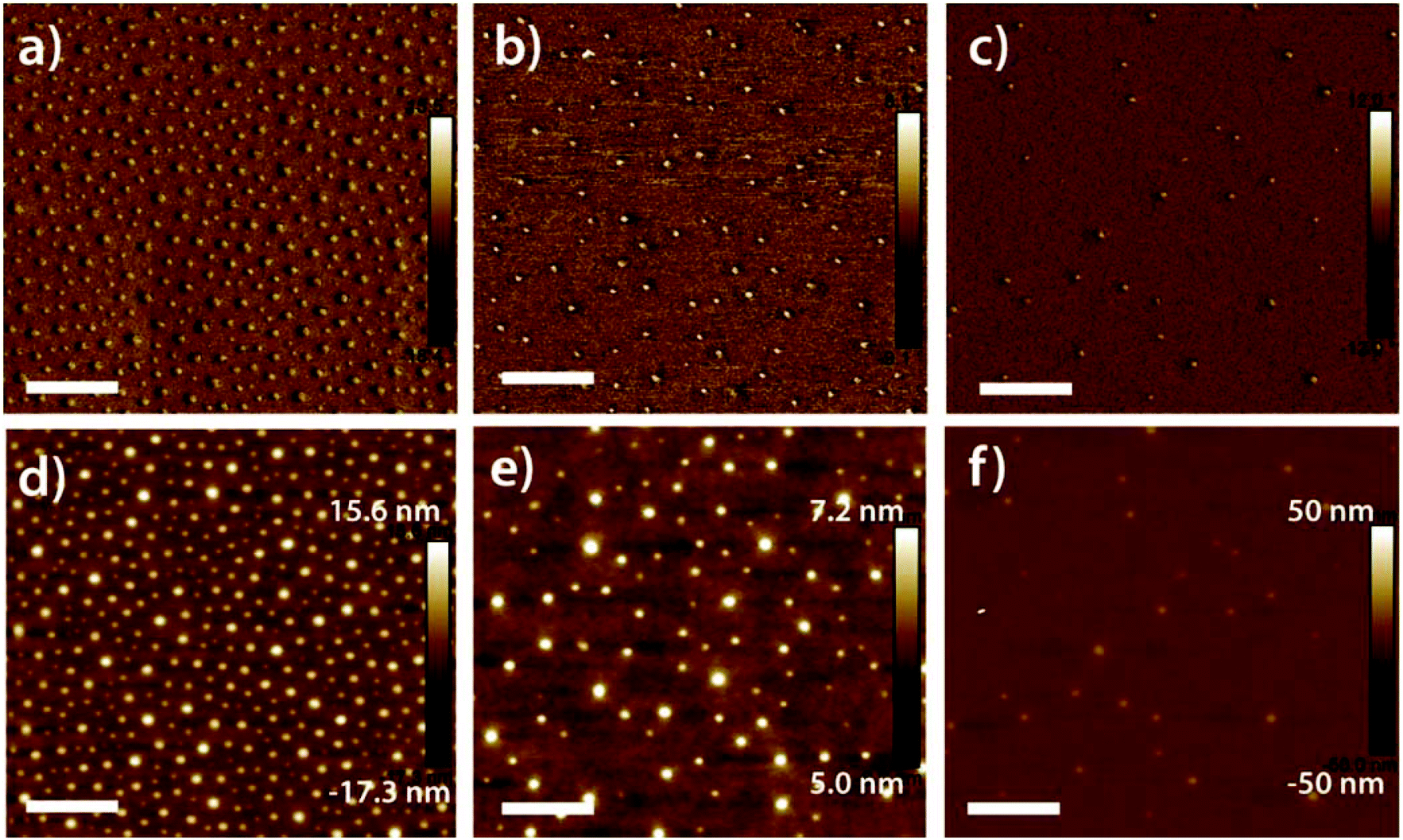
Scanning electron microscopy (SEM) images of nanorod arrays grown from the diluted micelle templates from Fig. 2 are shown in Fig. 3. SEM images of nanorod arrays grown from the neat BCP template can be found in ESI Fig. S2.† Top-down views (Fig. 3a–c) show the progressive increase in the average rod–rod distance, or decrease in the number density, as the BCP concentration in the film decreases. Angled views show ∼300 nm (Fig. 3d–f) and ∼1 μm long nanorods (Fig. 3g–i) produced by appropriate selection of the growth time, 20 and 45 minutes, respectively. Notably, the lateral dimensions of the nanorods did not change significantly during the extension of the growth time required to produce the 1 μm long rods, relative to the 300 nm case.
 | ||
| Fig. 3 Scanning electron microscopy images of ZnO nanorod arrays grown through 235/23 K PS-b-P4VP micelle templates diluted with 210 K PS homopolymer. Top-down views (a–c) and 70°-tilted views (d–f) of ∼300 nm tall arrays. (g–i) 70°-tilted views of ∼1 μm tall arrays. Dilutions are 2:1 (left), 4:1 (middle) and 9:1 (right). Scale bars are 1 μm. | ||
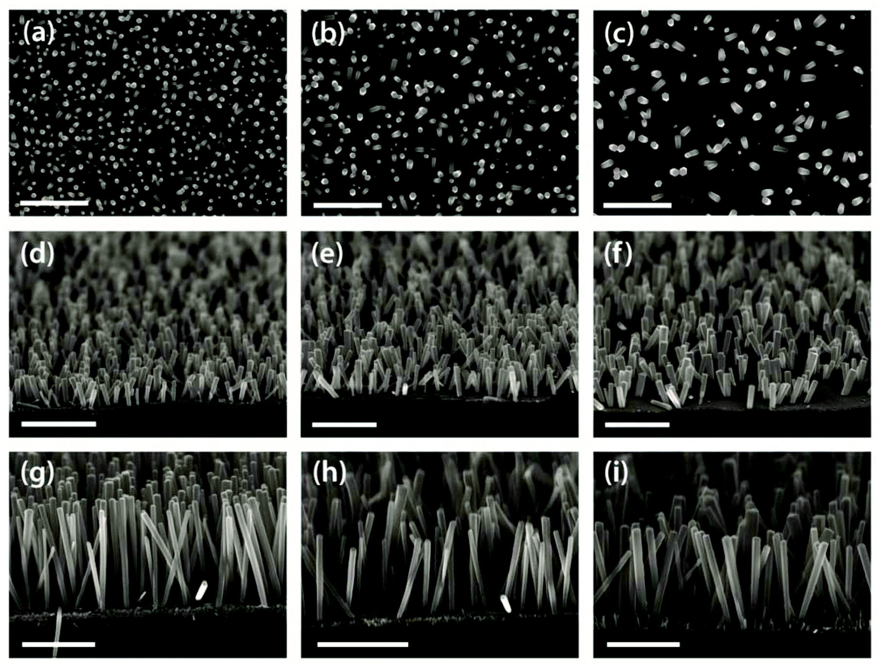
The nanorods are hexagonal in cross-section as expected for the ZnO wurtzite crystal structure. They display a characteristic UV absorption peak near 370 nm, consistent with the 3.37 eV band gap of ZnO, Fig. 4a. X-ray diffraction (XRD), Fig. 4b, shows peaks indexed to the ZnO structure with significant enhancement of the (002) reflection as commonly observed for high quality vertically oriented ZnO nanorods.32 The optical absorption data and XRD demonstrate, at a coarse level, the production of high quality ZnO nanomaterials, and that the structure and optoelectronic properties are not compromised by proximity to P4VP during growth.
 | ||
| Fig. 4 (a) UV-vis and (b) XRD of ∼1 micron-long nanorod arrays prepared from 235/23 K PS-b-P4VP micelles diluted to 4:1 HP:BCP with 210 K PS homopolymer by mass. | ||
SEM images of ∼300 nm tall nanorod samples were analyzed to determine the nanorod diameters and number densities, Fig. 5. The results show that the number density varies in direct proportion to the BCP concentration in the film, decreasing linearly from the value of the neat system, 100 μm−2 at CBCP = 1, to 8 μm−2 at CBCP = 0.1, Fig. 5d. The micelle core diameter dc = 35 nm. The separation s between nanorod surfaces varies from 62 nm for the neat system to 234 for the 9:1 dilution, as determined by the difference between the average rod–rod distance and the average rod diameter. The variation in the rod–rod distance (standard deviation) increases monotonically from about 10% for the non-diluted sample, to 25% for the highest dilution. We speculate that this may be due to the increasing importance of depletion interactions between the micelles due to the presence of increasing quantities of the homopolymer, leading to local clustering of the micelles.33 We anticipate that such variations can be minimized by suitable optimization of the molecular weight and polydispersity of the homopolymer, as well as processing steps to improve micelle spatial distribution after deposition. The experimentally measured average number densities vary on average by less than 5% from that expected based on the number density of the neat system and the concentration of the BCP, Fig. 5d. The strong agreement between observed and expected values highlights the fidelity of the templating process. On this basis we expect that further dilution will enable the production of arbitrarily low nanorod number densities.
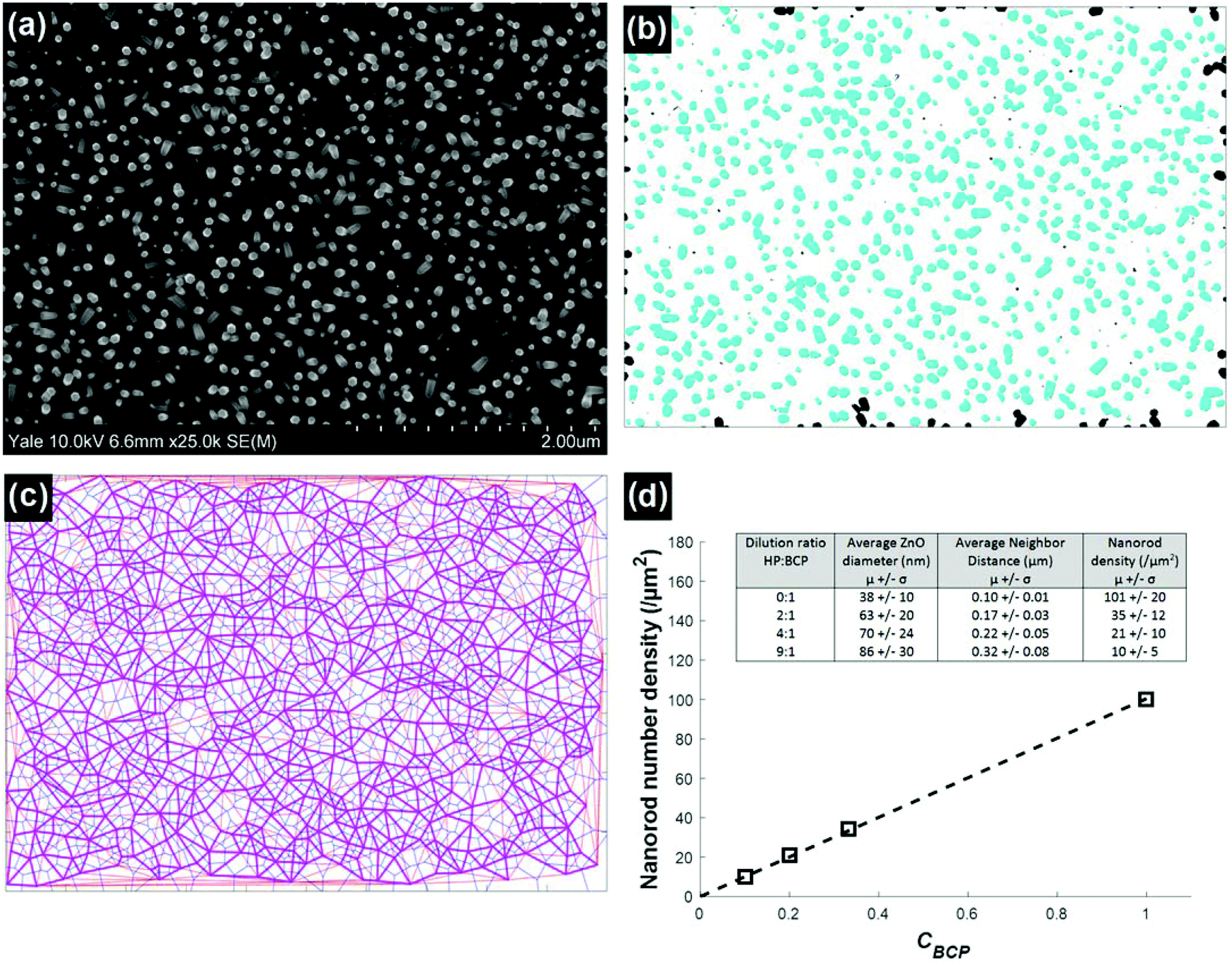 | ||
| Fig. 5 Analysis of SEM images to quantify nanorod arrays, and resulting metrics. (a) Original SEM image, in this case for a 4:1 dilution. (b) Image after thresholding, showing outline of nanorod cross-sections. (c) Voronoi tessellation (thin blue lines) and Delaunay triangulation applied to the thresholded image. Thick red lines represent nearest-neighbor connections. See ESI† for further details. (d) Nanorod number density as a function of block copolymer mass fraction in PS-b-P4VP micellar templates containing PS homopolymer. The line shows a linear fit to the data. Inset: summary of average and standard deviations of nanorod diameter and number density distributions for ∼300 nm-tall nanorods. | ||
We note that there is some increase in the diameter of the rods with decreasing BCP concentration, with nanorods varying from a diameter of 38 nm in the neat case to 86 nm in the 9:1 system. This is simply a consequence of the increase in the effective local concentration of reactant in the system as the number of active growth sites decreases with increasing homopolymer content. The nanorod diameter is in fact inversely proportional to the BCP concentration in the film. The standard deviation in the distribution of nanorod diameters varies over a small range, from about 25–30%. This is not atypical for hydrothermal synthesis of ZnO nanorods. Although we did not pursue it here, the nanorod diameter can be readily controlled independently by suitably adjusting the reaction conditions, including concentration of reactants, as well as the use of ionic additives.34
The thermophysical properties of the corona and HP polymer play key roles in dictating the rate of diffusion of reactants through the polymer film and the temperature limits for the reaction. While ZnO can be reliably grown rapidly to micron scale dimensions at temperatures as low as 70 °C, other metal oxide systems of interest require the use of higher temperatures, or longer reaction times. We experienced considerable difficulty in controlling the templating process and achieving reliably results at temperatures beyond ∼95 °C. We speculate that this is due to proximity to the glass transition temperature of PS, TPSg ∼ 100 °C. We expect that increasing mobility of the corona and HP chains on approaching TPSg degrades the fidelity of the process by enabling molecular motion, as well as decreasing the disparity in transport between the PS and P4VP. Further, we observed dewetting of the HP:BCP film at extended reaction times even at lower temperatures, although such dewetting appeared to take place well after the growth phase of the reaction, and therefore did not affect templating. Nevertheless it reinforces the notion that the Tg can constrain the conditions under which templating can be reasonably performed.
We explored the use of a HP:BCP system with a higher Tg as a means to circumvent the limitations described above. We used poly(α-methyl styrene-block-4-vinyl pyridine) (Pα-MeS-b-P4VP) (Mn Pα-MeS/Mn P4VP = 13 kDa/24 kDa) mixed with Pα-MeS homopolymer (Scientific Polymer Products) (11.8 kDa). The glass transition temperature of Pα-MeS is 170 °C, significantly higher than that of PS. The same protocols were applied for sample preparation except that HP:BCP solutions were prepared at 1 wt%, and spin coating was performed at 4k rpm. We determined that growth could be conducted successfully with no loss of templating up to 95 °C but did not explore higher temperatures due to practical concerns regarding the boiling of the growth solution. A standard growth temperature of 80 °C was adopted to generate the data shown here. The resulting nanorod densities and diameters are shown in Fig. 6. AFM images of 9:1 HP:BCP dilutions are shown in ESI Fig. S3.† SEM images of nanorod arrays templated from diluted Pα-MeS-b-P4VP are provided in ESI Fig. S4.† The data again show a linear correlation between nanorod density and BCP concentration. Here we restricted consideration to dilutions sufficient to provide final densities from ∼10 to 100 μm−2. The variation of the rod–rod distance was similar to the PS-b-P4VP case, though we note that the standard deviation of the nanorod diameter distribution was reduced. This may be a consequence of better confinement afforded by the higher Tg corona chains of Pα-MeS relative to PS. Templates prepared using Pα-MeS-b-P4VP displayed improved thermal stability relative to PS-b-P4VP (ESI Fig. S4b†). After growth and rinsing, the polymer film was readily visible, intact and conformal, atop the seed layer, with ZnO nanorods protruding from the film surface. This was also the case for growth in near-boiling conditions. We can therefore envision the retention of the film in a device to serve a secondary function, such as serving as a blocking layer, or providing separation and protection of an underlying surface.
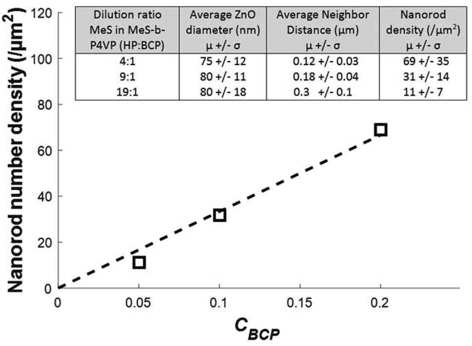 | ||
| Fig. 6 Nanorod number density as a function of block copolymer mass fraction in Pα-MeS diluted Pα-MeS-b-P4VP micellar templates. The line shows a linear fit to the data. Inset: summary of average nanorod diameter and number density for ∼300 nm-tall nanorods. | ||
There is a wide range of applications that can be enabled by the tailored fabrication of ZnO nanorod arrays. Such arrays have been successfully employed as templates for other functional materials of interest including TiO2 nanotubes35 and Au nanorods,36,37 and may also be used as low-cost sacrificial templates for nanoimprint lithography. Au nanorod arrays which act as plasmonic metamaterials have been successfully used for highly sensitive biosensing, with the plasmon guiding mode dictated by the average nanorod spacing.28 Solvothermally produced ZnO nanorods may be substitutionally doped to improve photoelectrochemical water splitting function38 or to enhance conductivity in use as transparent oxide electrodes.39 We expect the synthesis of other functional oxides such as ZrO2,40 Co3O4,41 SnO2,42 and WO343 can be reasonably adapted to produce nanorod arrays using the micelle templating approach demonstrated here. This opens the doors to a large number of applications including biological scaffolds, heterogeneous catalysts, supercapacitors, and battery electrodes.
Where required, the average distance between nanorod surfaces can be precisely specified as described in eqn (1). This is particularly relevant for quantum dot solar cells and sensors based on optical resonances of visible light. The relevant length scales in those scenarios, ∼100–500 nm are readily accessible using the method reported here. The variation in the rod–rod spacing should be taken into account when considering the application of these nanorod arrays. Different applications would exhibit different sensitivities, which should be appropriately considered. For example in plasmonic sensing, the plasmon propagating mode properties are a function of the average rod–rod spacing and are not overly sensitive to local variations therefrom. In photovoltaics the situation is different as local variations would result in local changes in charge extraction efficiency that could sum to make a meaningful difference in the overall device operation. Finally, it is worth noting that the molecular weight of the homopolymer used should be close to that of the corona chains. The use of much lower molecular weight chains leads to excessively fast diffusion of reactants to the substrate and loss of templating fidelity. Conversely, excessively high molecular weight chains lead to micelle aggregation, apparently due to depletion interactions33 (ESI Fig. S5†).
In conclusion, we have demonstrated a robust and scalable method for controlling the areal density of nanorod arrays produced by BCP micelle templated solvothermal synthesis. This provides a needed complement to existing methods such as those based on interference lithography, or colloidal particle templating.44,45 Nanorod densities ranging from ∼10–100 μm−2 were demonstrated here, though there is no intrinsic limitation on how low a density can be achieved. The use of higher Tg materials permits this approach to be used in a wider range of syntheses, or to preserve the template film for use in the device. The ability to produce nanorod arrays readily over large areas allows one to envision low-cost and rapid fabrication of nanostructured electrodes with geometries tailored to specific applications. We anticipate also that nanorod arrays fabricated in this way will enable simpler experimental studies relating the role of electrode feature size and spacing on device properties of interest.
Acknowledgements
This work was supported by Office of Naval Research (N000141210657) and NSF (CMMI-1246804). C. P. acknowledges financial support from the NSF Graduate Research Fellowship Program (GRFP). K. T. also acknowledges support from NSF GRFP (DGE-1122492). Facilities use was supported by YINQE and NSF MRSEC DMR-1119826. The authors gratefully acknowledge J. Singer for helpful discussions.Notes and references
- R.-E. Nowak, M. Vehse, O. Sergeev, T. Voss, M. Seyfried, M. von Maydell and C. Agert, Adv. Opt. Mater., 2013, 2, 94–99 CrossRef.
- U. W. Paetzold, S. Lehnen, K. Bittkau, U. Rau and R. Carius, Nano Lett., 2014, 14, 6599–6605 CrossRef CAS PubMed.
- E.-Z. Tan, P.-G. Yin, T.-t. You, H. Wang and L. Guo, ACS Appl. Mater. Interfaces, 2012, 4, 3432–3437 CAS.
- L. Whittaker-Brooks, W. E. McClain, J. Schwartz and Y.-L. Loo, Adv. Energy Mater., 2014, 4, 1400585 Search PubMed.
- K. Takanezawa, K. Hirota, Q.-S. Wei, K. Tajima and K. Hashimoto, J. Phys. Chem. C, 2007, 111, 7218–7223 CAS.
- A. B. F. Martinson, J. E. McGarrah, M. O. K. Parpia and J. T. Hupp, Phys. Chem. Chem. Phys., 2006, 8, 4655–4659 RSC.
- C. I. Pelligra, P. W. Majewski and C. O. Osuji, Nanoscale, 2013, 5, 10511–10517 RSC.
- S. Zhang, C. I. Pelligra, G. Keskar, J. Jiang, P. W. Majewski, A. D. Taylor, S. Ismail-Beigi, L. D. Pfefferle and C. O. Osuji, Adv. Mater., 2012, 24, 82–87 CrossRef CAS PubMed.
- J. Jean, S. Chang, P. R. Brown, J. J. Cheng, P. H. Rekemeyer, M. G. Bawendi, S. Gradecak and V. Bulovic, Adv. Mater., 2013, 25, 2790–2796 CrossRef CAS PubMed.
- C. Cao, C. Hu, X. Wang, S. Wang, Y. Tian and H. Zhang, Sens. Actuators, B, 2011, 156, 114–119 CrossRef CAS.
- L. E. Greene, M. Law, D. H. Tan, M. Montano, J. Goldberger, G. Somorjai and P. Yang, Nano Lett., 2005, 5, 1231–1236 CrossRef CAS PubMed.
- L. Baeten, B. Conings, J. D'Haen, C. Dobbelaere, A. Hardy, J. V. Manca and M. K. Van Bael, Chem. Phys. Phys. Chem., 2012, 13, 2777–2783 CAS.
- J. Liu, J. She, S. Deng, J. Chen and N. Xu, J. Phys. Chem. C, 2008, 112, 11685–11690 CAS.
- T. Ma, M. Guo, M. Zhang, Y. Zhang and X. Wang, Nanotechnology, 2007, 18, 035605 CrossRef PubMed.
- B. Conings, L. Baeten, H.-G. Boyen, J. D'Haen, M. K. Van Bael and J. V. Manca, J. Phys. Chem. C, 2012, 116, 14237–14242 CAS.
- B. Weintraub, S. Chang, S. Singamaneni, W. H. Han, Y. J. Choi, J. Bae, M. Kirkham, V. V. Tsukruk and Y. Deng, Nanotechnology, 2008, 19, 435302 CrossRef PubMed.
- X.-D. Gao, X.-M. Li, W.-D. Yu, L. Li and J.-J. Qiu, Appl. Surf. Sci., 2007, 253, 4060–4065 CrossRef CAS.
- J. J. Richardson, D. Estrada, S. P. DenBaars, C. J. Hawker and L. M. Campos, J. Mater. Chem., 2011, 21, 14417–14419 RSC.
- D. Andeen, J. H. Kim, F. F. Lange, G. K. L. Goh and S. Tripathy, Adv. Funct. Mater., 2006, 16, 799–804 CrossRef CAS.
- H. Chik, J. Liang, S. G. Cloutier, N. Kouklin and J. M. Xu, Appl. Phys. Lett., 2004, 84, 3376–3378 CrossRef CAS.
- W. Hwang, J.-H. Choi, T. H. Kim, J. Sung, J.-M. Myoung, D.-G. Choi, B.-H. Sohn, S. S. Lee, D. H. Kim and C. Park, Chem. Mater., 2008, 20, 6041–6047 CrossRef CAS.
- E. Pal, A. Oszko, P. Mela, M. Moller and I. Dekany, Colloids Surf., A, 2008, 331, 213–219 CrossRef CAS.
- S. I. Yoo, B.-H. Sohn, W.-C. Zin, S.-J. An and G.-C. Yi, Chem. Commun., 2004, 2850–2851 RSC.
- C. I. Pelligra, S. Huang, J. P. Singer, A. T. Mayo, R. R. Mu and C. O. Osuji, Small, 2014, 10, 4304–4309 CAS.
- J.-H. Kim, S.-S. Kim and B.-H. Sohn, J. Mater. Chem. C, 2015, 3, 1507–1512 RSC.
- I. J. Kramer, D. Zhitomirsky, J. D. Bass, P. M. Rice, T. Topuria, L. Krupp, S. M. Thon, A. H. Ip, R. Debnath, H.-C. Kim and E. H. Sargent, Adv. Mater., 2012, 24, 2315–2319 CrossRef CAS PubMed.
- X. Lan, S. Masala and E. H. Sargent, Nat. Mater., 2014, 13, 233–240 CrossRef CAS PubMed.
- A. V. Kabashin, S. Pastkovsky, W. Hendren, G. A. Wurtz, R. Atkinson, R. Pollard, V. A. Podolskiy and A. V. Zayats, Nat. Mater., 2009, 8, 867–871 CrossRef CAS PubMed.
- Y. Jin, Adv. Mater., 2012, 24, 5153–5165 CrossRef CAS PubMed.
- M. R. Jones, K. D. Osberg, R. J. Macfarlane, M. R. Langille and C. A. Mirkin, Chem. Rev., 2011, 111, 3736–3827 CrossRef CAS PubMed.
- J. Elias, R. Tena-Zaera, G.-Y. Wang and C. Levy-Clement, Chem. Mater., 2008, 20, 6633–6637 CrossRef CAS.
- J.-J. Wu and S.-C. Liu, Adv. Mater., 2002, 14, 215 CrossRef CAS.
- S. Abbas and T. P. Lodge, Phys. Rev. Lett., 2007, 99, 137802 CrossRef PubMed.
- J. Joo, B. Y. Chow, M. Prakash, E. S. Boyden and J. M. Jacobson, Nat. Mater., 2011, 10, 596–601 CrossRef CAS PubMed.
- J. Qiu, W. Yu, X. Gao and X. Li, Nanotechnology, 2006, 17, 4695–4698 CrossRef CAS PubMed.
- L. Chen, L. Luo, Z. Chen, M. Zhang, J. A. Zapien, C. S. Lee and S. T. Lee, J. Phys. Chem. C, 2010, 114, 93–100 CAS.
- Z. H. Chen, Y. B. Tang, C. P. Liu, Y. H. Leung, G. D. Yuan, L. M. Chen, Y. Q. Wang, I. Bello, J. A. Zapien, W. J. Zhang, C. S. Lee and S. T. Lee, J. Phys. Chem. C, 2009, 113, 13433–13437 CAS.
- X. Yang, A. Wolcott, G. Wang, A. Sobo, R. C. Fitzmorris, F. Qian, J. Z. Zhang and Y. Li, Nano Lett., 2009, 9, 2331–2336 CrossRef CAS PubMed.
- S. Yun, J. Lee, J. Yang and S. Lim, Physica B, 2010, 405, 413–419 CrossRef CAS.
- Z. Lu, Z. Zhu, J. Liu, W. Hu and C. M. Li, Nanotechnology, 2014, 25, 215012 Search PubMed.
- J. Jiang, J. P. Liu, X. T. Huang, Y. Y. Li, R. M. Ding, X. X. Ji, Y. Y. Hu, Q. B. Chi and Z. H. Zhu, Cryst. Growth Des., 2010, 10, 70–75 CAS.
- L. Vayssieres and M. Graetzel, Angew. Chem., Int. Ed., 2004, 43, 3666–3670 CrossRef CAS PubMed.
- S. S. Kalanur, Y. J. Hwang, S. Y. Chae and O. S. Joo, J. Mater. Chem. A, 2013, 1, 3479–3488 CAS.
- J. J. Dong, X. W. Zhang, Z. G. Yin, S. G. Zhang, J. X. Wang, H. R. Tan, Y. Gao, F. T. Si and H. L. Gao, ACS Appl. Mater. Interfaces, 2011, 3, 4388–4395 CAS.
- Y. Wei, W. Wu, R. Guo, D. Yuan, S. Das and Z. L. Wang, Nano Lett., 2010, 10, 3414–3419 CrossRef CAS PubMed.
Footnote |
| † Electronic supplementary information (ESI) available. See DOI: 10.1039/c5nr07914d |
| This journal is © The Royal Society of Chemistry 2016 |