
Inkjet-printed all solid-state electrochromic devices based on NiO/WO3 nanoparticle complementary electrodes†
Guofa
Cai
a,
Peter
Darmawan
a,
Mengqi
Cui
a,
Jingwei
Chen
a,
Xu
Wang
a,
Alice Lee-Sie
Eh
a,
Shlomo
Magdassi
b and
Pooi See
Lee
*a
aSchool of Materials Science and Engineering, Nanyang Technological University, 639798, Singapore. E-mail: pslee@ntu.edu.sg
bInstitute of Chemistry and the Center for Nanoscience and Nanotechnology, The Hebrew University of Jerusalem, Jerusalem, 91904, Israel
First published on 16th November 2015
Abstract
Nanostructured thin films are important in the fields of energy conversion and storage. In particular, multi-layered nanostructured films play an important role as a part of the energy system for energy saving applications in buildings. Inkjet printing is a low-cost and attractive technology for patterning and deposition of multi-layered nanostructured materials on various substrates. However, it requires the development of a suitable ink formulation with optimum viscosity, surface tension and evaporation rate for various materials. In this study, a versatile ink formulation was successfully developed to prepare NiO and WO3 nanostructured films with strong adhesion to ITO coated glass using inkjet printing for energy saving electrochromic applications. We achieved a high performance electrochromic electrode, producing porous and continuous electrochromic films without aggregation. The NiO film with 9 printed layers exhibits an optical modulation of 64.2% at 550 nm and a coloration efficiency (CE) of 136.7 cm2 C−1. An inkjet-printed complementary all solid-state device was assembled, delivering a larger optical modulation of 75.4% at 633 nm and a higher CE of 131.9 cm2 C−1 among all solid-state devices. The enhanced contrast is due to the printed NiO film that not only performs as an ion storage layer, but also as a complementary electrochromic layer.
1. Introduction
With the increasing energy demand, there has been growing interest in the search for methods to reduce energy consumption.1–6 Electrochromism is a promising energy-saving and energy-conversion technology which can reversibly and persistently change their optical properties to intelligently control the amount of solar heat in response to changes in ambient temperature by electrochemical oxidation and reduction of the electrochromic materials.7–9 An electrochromic device is a multilayered structure consisting of a transparent conductor, an electrochromic film, an ion conductor and an ion storage film. These devices attract considerable attention because of their potential applications, such as smart windows for energy efficient building, information displays, self-dimming rear mirrors for automobiles, electronic papers and switchable mirrors.10–13 A large optical modulation, good optical memory and chemical stability are required for a high-performance electrochromic device. Nickel oxide (NiO) is known as one of the most popular anodic electrochromic materials and tungsten trioxide (WO3) as one of the widely accepted cathodic electrochromic materials, both of which have been intensively investigated.14–16 NiO and WO3 are complementary electrode materials when they are integrated into one electrochromic device using lithium based electrolytes. They can be simultaneously colored and bleached with opposite polarity, therefore, increasing the optical modulation of the complementary device.The usual methods for producing electrochromic nanostructured NiO and WO3 films include sputtering,17,18 electrodeposition19,20 and hydrothermal processing.21,22 Unfortunately, these methods do not meet the requirements of low cost and versatile processing for consumable electronic systems. Furthermore, additional requirements are imposed on the emerging electronic development, such as the need for patterning and multi-layered structures. In the past, creation of specific patterns usually involves a subtractive approach such as an expensive lithography process or additional masking steps, which results in the wasting of materials or high cost during the fabrication process. Inkjet printing is a low-cost and attractive additive manufacturing technology for patterning electrochromic materials on various substrates and allows deposition of electrochromic materials on a specific location with simultaneous thickness control by the number of printed layers. In addition, inkjet printing can be further integrated with the roll-to-roll technology for industrial scale production.23,24 However, inkjet printing requires the development of versatile ink formulation with optimum viscosity, surface tension and evaporation rate to avoid formation of inhomogeneous films, irregular and deformed printed lines, cracks and so on. Despite the prior effort of inkjet patterning of NiO on a thermistor25 and multilayered ceramic,26 demonstration of inkjet printed NiO for electrochromics has not been realized before. With our earlier established work on inkjet patterning of WO3 for electrochromic application,27 we extended our efforts on the understanding of the effects of inkjet printing parameters such as the number of printed layers and the annealing temperature on the electrochromic performance. In addition, although a few papers about inkjet-printed electrochromic devices were published recently, the devices were assembled by the same electrochromic materials on single or both electrodes and the optical modulation is still unsatisfactory.28–31 Herein, we report the first inkjet-printed complementary all solid-state electrochromic device with one of the best performances to date, to the best of our knowledge.
We introduce a versatile ink formulation and prepare electrochromic NiO and WO3 films by inkjet printing technique. The ink formulation can work well for both NiO and WO3 nanoparticles. The electrochromic performances of the NiO films with increasing printed layers and various thermal treatment temperatures are investigated in detail. Subsequently, an all solid electrochromic device was assembled with a NiO film as an ion storage layer, a WO3 film as an electrochromic layer and poly(methyl methacrylate) (PMMA)-based polymer electrolytes as solid electrolytes. A solid-state electrochromic device can avoid the electrolyte leakage problem, allowing the ease of handling, reducing the cost of device packaging and attaining greater reliability. In order to be consistent with the already existing electrochromic window in some energy efficient building, the commercial indium tin oxide (ITO)-coated glass was used as the conductive transparent substrate. The resulting electrochromic device with the inkjet printed NiO film as an ion storage layer exhibits a large optical modulation and high coloration efficiency.
2. Experimental section
tert-Butanol (anhydrous, ≥99.5%), nickel acetylacetonate (95% purity), metallic tungsten, hydrogen peroxide (30%), PMMA (Mw = 996![[thin space (1/6-em)]](https://www.rsc.org/images/entities/char_2009.gif) 000), propylene carbonate (PC, ≥99.7%), lithium perchlorate (LiClO4, ≥95.0%), ethylene glycol (EG, ≥99.5%), acetonitrile (ACN, ≥99.8%) and diethylene glycol n-butyl ether (DB, ≥99%) were purchased from Sigma-Aldrich. All the chemicals were used without further purification.
000), propylene carbonate (PC, ≥99.7%), lithium perchlorate (LiClO4, ≥95.0%), ethylene glycol (EG, ≥99.5%), acetonitrile (ACN, ≥99.8%) and diethylene glycol n-butyl ether (DB, ≥99%) were purchased from Sigma-Aldrich. All the chemicals were used without further purification.
2.1 Ink formulation
The NiO nanoparticles were prepared according to the method of our previous work.32 In brief, 0.39 g nickel acetylacetonate was added into 42 ml tert-butanol under stirring, forming a light green suspension. Thereafter, the obtained solution was transferred into a Teflon lined stainless autoclave, and then the autoclave was sealed and heated at 200 °C for 24 h. Afterwards, the autoclave was cooled to room temperature under air cooling. Finally, the NiO precipitates in the solution were collected and dried in an oven at 60 °C. The WO3 nanoparticles were synthesized based on a modified sol–gel route according to Costa et al.,29 and as reported in our previous work.27 The NiO ink follows a similar formulation as the WO3 ink, with DB, EG and DI water as the solvents (NiO:EG:DB:DI water = 1:2:47:50). The optimized concentration of the NiO is 1 wt% in the ink (beyond this concentration there will be sedimentation after a few days). The surface tension and the viscosity of the NiO ink are 22.51 Nm m−1 and 6.59 cP, respectively. Both inks were stable under ambient conditions for several weeks without particle sedimentation and aggregation, and displayed good printability.
2.2 Solid polymer electrolyte preparation
An electrolyte casting solution was prepared by adding ACN and PC via a syringe into a blue cap bottle containing LiClO4. Then PMMA was slowly added into the solution, followed by stirring at 60 °C for 12 h. The gel electrolyte is formed with a weight percent composition of 61:17:7:15 (ACN:PC:LiClO4:PMMA). After assembling the device, the gel electrolyte will change to a solid electrolyte after naturally dried in air for 2 h.
2.3 Sample characteristics
The surface tension and viscosity of the ink were analyzed by using Kibron Ez-Pi Plus and a Brookfield viscometer, respectively. An X-ray diffractometer (XRD, a Bruker D8 Discover diffractometer with Ni-filtered Cu Kα-radiation (λ = 1.5406 Å)), a transmission electron microscope (TEM, JEOL 2010), a scanning electron microscope (SEM, JEOL 7600F), and an optical microscope (Olympus SZ61) were used to characterize the morphology, structure and composition of the products. The adhesion strength was evaluated according to ASTM D3359, the standard test methods for measuring the adhesion by tape testing. X-ray photoelectron spectroscopy (XPS) analysis of the NiO and WO3 powders was performed using the VG ESCALab 220i-XL Imaging XPS last calibrated in March 2015. A monochromatic Al Kα X-ray gun (hν = 1486.7 eV) was employed using a large area lens mode for analysis with a photoelectron take-off angle of 90° with respect to the surface plane. The maximum analysis depth lies in the range of 4–8 nm. The error of binding energy is estimated to be within ±0.2 eV.2.4 Electrochemical characterization
Electrochemical measurements of NiO films were performed on a Solatron 1470E. The transmission spectra of NiO thin films and the solid device in the fully colored and fully bleached states were measured on a SHIMADZU UV-3600 spectrophotometer over the wavelength range from 300 to 900 nm.3. Results and discussion
3.1 Microstructure characteristics
To determine the crystal structure and phase information of the NiO and the WO3 powder, the XRD patterns were collected from both samples as shown in Fig. 1a. The XRD spectra of the synthesized NiO powder exhibit diffraction peaks at 2θ degrees of 37.78°, 43.31°, 62.74°, 75.49° and 79.49°, which can be assigned to the (111), (200), (220), (311) and (222) reflections of the cubic NiO phase (JCPDS 00-047-1049), respectively. The synthesized WO3 powder shows characteristic diffraction peaks that can be readily indexed to a mixture of hexagonal and orthorhombic WO3·0.33H2O (JCPDS 00-035-1001 and 00-035-0270). XPS measurements were performed to analyze the binding energy and oxidation state of the NiO and the WO3 powder. Fig. 1b shows the high resolution Ni 2p XPS spectrum of the NiO powder. The Ni 2p3/2 peak includes two components, one peak at 854 eV due to Ni2+ in the Ni–O bonds and another peak at 856 eV due to the Ni–OH bonds, respectively.33,34 The Ni–OH bonds mainly originate from NiOOH or tert-butanol groups attached to the surface of NiO.35 It illustrates that the powder present is mainly NiO, and possibly contains a small amount of NiOOH on the surface of NiO nanoparticles. There are spin–orbit doublets in the high resolution XPS spectrum of the W 4f peak, corresponding to W 4f7/2, W 4f5/2 and W 5p3/2 peaks which are located at 35.7 eV, 37.8 eV and 41.5 eV, respectively (Fig. 1c). These results match well with those reported in the previous literature for WO3.36,37Fig. 1d and e present the TEM images of the NiO and WO3 powders, respectively. The NiO nanoparticles show non-agglomerated, defined particles with a particle size distribution of 30–50 nm (Fig. 1d). The HRTEM image shows that the lattice fringes with the interplanar spacings of d200 = 0.21 nm are clearly imaged, consistent with the cubic rock salt structure of NiO deduced from XRD patterns. Fig. 1e shows that the WO3 nanoparticles are quasi-oblong in shape, and the sizes vary from 50 to 120 nm. The lattice fringe distances of 0.32 nm in the HRTEM image is in agreement with the d-spacings of the (200) planes of hexagonal WO3·0.33H2O. It is worth noting that both NiO and WO3 particle sizes are suitable for inkjet printing applications with the typical nozzle diameter in the range of tens of micrometers. The surface morphologies of the NiO and the WO3 films printed on the ITO glass are shown in the SEM images of Fig. 1f and g, respectively. Uniform particles with a compact smooth surface are observed in the printed NiO film (Fig. 1f). The printed WO3 film is assembled from many smaller nanoparticles (Fig. 1g). The thickness of the printed films is proportionally increased by increasing the number of printed layers. The thickness of the printed NiO films with 1, 2 and 3 layers is 170, 335 and 530 nm as shown in Fig. S1a–c in the ESI,† respectively. In addition, the thickness of the printed WO3 films (5 wt%) with 1 layer is 218 nm. The adhesion of the printed films on the ITO substrate was studied using the standard American Society for Testing and Materials Procedure (ASTM D3359), in which ASTM 0B and 5B represent the worst and the highest adhesion grade, respectively. Fig. S2a† shows the optical microscopy image of WO3 films on the ITO glass after the tape test. The edges of the cuts are completely smooth and none of the squares of the lattice is detached. Therefore, the film exhibited the highest adhesion grade of 5B. From the SEM image (Fig. S2b†), it can be seen that there is no obvious change for the WO3 film after the tape test, the WO3 nanoparticles remained in the original positions and maintained their shapes on the ITO substrate, which indicates that the printed films exhibit strong adhesion with the ITO glass.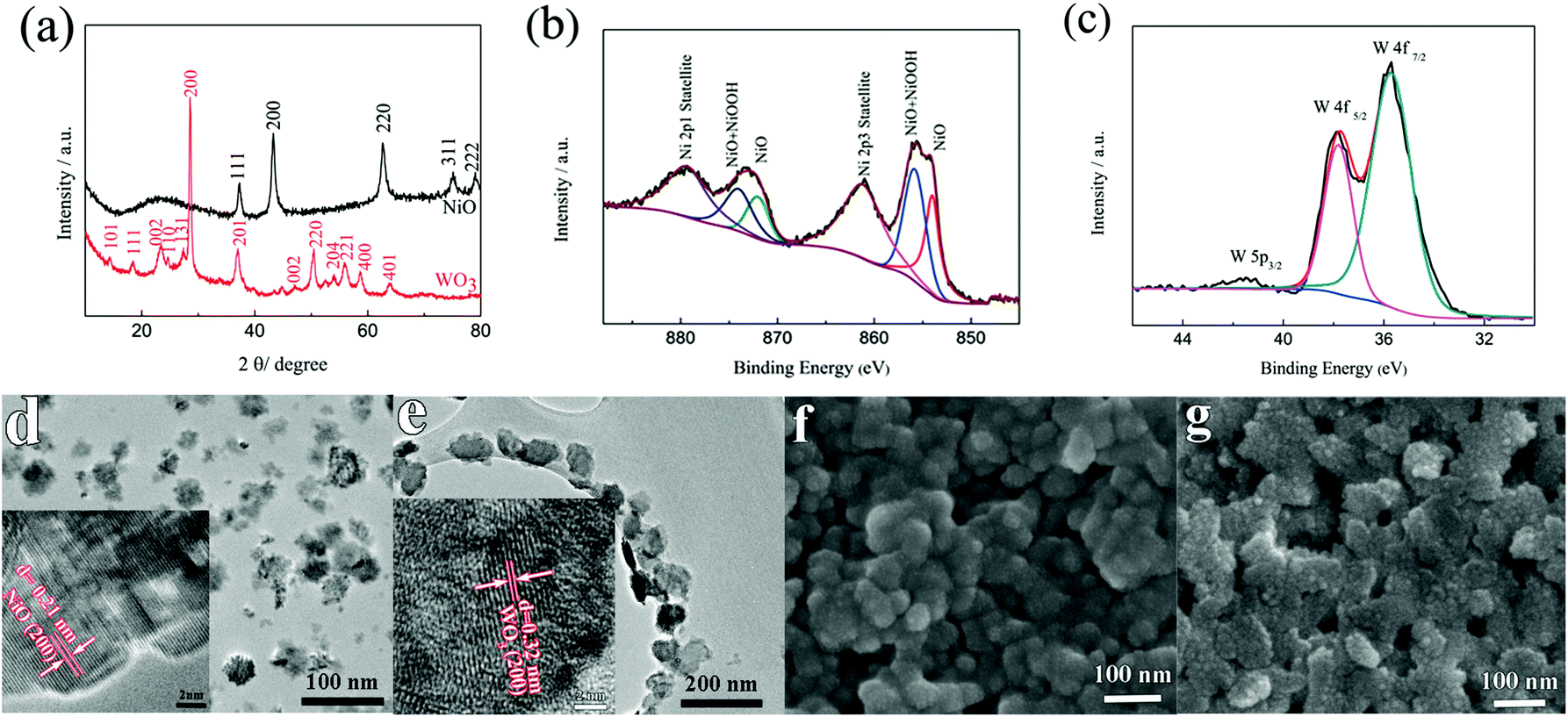 | ||
| Fig. 1 (a) XRD patterns of the NiO and WO3 powders, (b) Ni 2p XPS spectra of the NiO powder, (c) W 4f XPS spectrum of the WO3 powder, low magnification and high magnification TEM images of the (d) NiO and (e) WO3 powders, and SEM images of the printed (f) NiO and (g) WO3 films. | ||
3.2 Electrochemical performance evaluations
The electrochromic properties of the printed NiO films with different layers were measured in a three-electrode electrochemical cell containing 1 M KOH aqueous solution as the electrolyte. The printed NiO films were used as the working electrode, a Pt wire was used as the counter electrode and an Ag wire was used as the reference electrode. The transmittance of the ITO glass in the electrolyte was considered to be 100% and was used as the baseline. The color of the NiO films changed from transparent (bleached state) to brown (colored state) while applying step voltages of −0.2 and 0.6 V (vs. Ag wire). The coloration and bleaching process of the NiO films can be attributed to the following electrochemical reactions:| NiO + OH− ↔ NiOOH + e− | (1) |
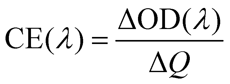
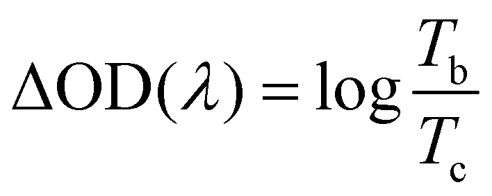
The transmittance spectra of the printed NiO films with different layers in the colored and bleached states in the wavelength range of 300–900 nm are shown in Fig. 2a. It is clearly seen that the transmittance of the NiO films in both colored and bleached states decreases with increasing the number of NiO layers, and the optical modulation increases linearly with increasing the number of NiO layers within 3 layers (Fig. 2b). However, the optical modulation decreases dramatically for the printed NiO over 3 layers, because the films can hardly be bleached due to the thick dense layer in the presence of an organic binder with a larger amount of NiO nanoparticles. The switching speed from one state to another state under an alternating potential is an important factor in electrochromic devices. Herein, the switching time is defined as the time required for a system to reach 90% of its full optical modulation. The coloration and bleaching times of the printed NiO films with different layers are investigated by employing chronoamperometry (CA) and the corresponding in situ transmittance at 550 nm, as shown in Fig. 2c and S3.† It can be clearly seen that both switching times generally increase with increasing the number of NiO layers, and the coloration time is shorter than the bleaching time for all the films, which illustrates that the coloration process is easier than the bleaching process for all the printed NiO films. Coloration efficiency (CE) is another important criterion often used to characterize an electrochromic material, which is defined as the ratio of optical density change (ΔOD) of the film at a certain wavelength and the corresponding injected (or ejected) charge density (Q) per unit area. It can be calculated according to the following equation:
 | (2) |
 | (3) |
 | ||
| Fig. 2 (a) Optical transmittance spectra at colored and bleached states, (b) corresponding to transmittance modulations, (c) coloration time and bleaching time and (d) CE values of the printed NiO films with different layers. | ||
Based on the above results, the optical modulation and CE of the printed NiO films does not increase continuously with the number of NiO layers due to the restricted bleaching process of thick NiO films in the presence of an organic binder, which can retard the diffusion of the electrolyte into the thick NiO layer. The increasing number of NiO printed layers is beneficial to the electrochromic performance within 3 layers; however, the continuous increasing of NiO printed layers causes an adverse effect on the electrochromic performance after 3 layers.
In order to verify this, the printed NiO films with 6 layers which have undergone annealing at different temperatures for 2 h were further investigated. The SEM images of the films after annealing at different temperatures are shown in Fig. 3. The exposure of pristine NiO particles of the film annealed at 150 °C was due to the partial evaporation of the organic solvent and thus the film exhibits a porous structure (Fig. 3a). After annealing at 200 °C, most of the organic solvent evaporated and uniform NiO nanoparticles were left behind as shown in Fig. 3b. However, the NiO nanoparticles begin to aggregate when the annealed temperature is up to 250 °C (Fig. 3c) and the NiO nanoparticles show strong agglomeration after annealing at 300 °C (Fig. 3d). To determine the crystal structure and possible phase changes during the annealing process, XRD patterns are collected from the films after annealing at various temperatures as shown in Fig. S4.† It can be clearly seen that the diffraction peaks of the films remain unchanged. After subtracting the diffraction peaks of the substrates, the diffraction peaks at 2θ degrees of 37.78°, 43.31° and 62.74° can be assigned to the (111), (200) and (220) reflections of the cubic NiO phase, respectively.
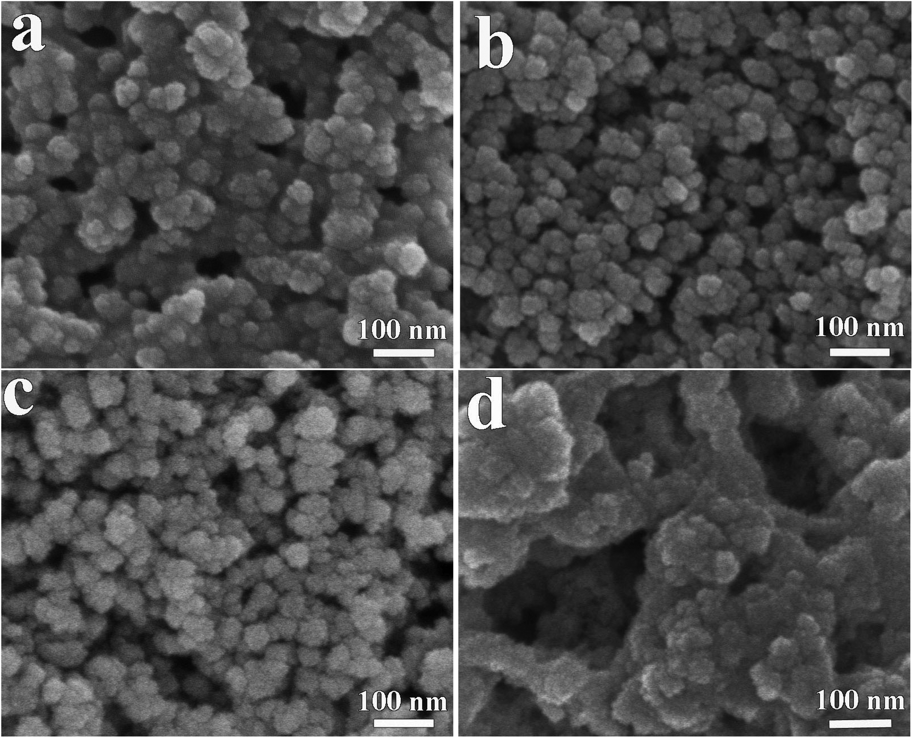 | ||
| Fig. 3 SEM images of the printed NiO films with 6 layers which have undergone annealing at (a) 150 °C, (b) 200 °C, (c) 250 °C and (d) 300 °C for 2 h. | ||
The electrochromic properties of the printed NiO films with 6 layers after annealing at different temperatures for 2 h were further measured in the three-electrode electrochemical cell. Fig. 4a shows the transmittance spectra of the printed NiO films with 6 layers after annealing at different temperatures for 2 h in the colored and bleached states in the wavelength range of 300–900 nm. It can be seen that the transmittance of the NiO films in both the colored and bleached states increases with increasing the annealing temperature due to the evaporation of the organic solvent and the decomposition of the organic binder, leading to an active electrochemical reaction of NiO with the electrolyte. The optical modulation increases with increasing the annealing temperature within 200 °C, and then decreases when the annealed temperature is over 200 °C (Fig. 4b). A higher annealing temperature typically leads to the formation of compact crystalline NiO.38,39 A fully crystalline and agglomerated film is considered too dense for ion intercalation, thus resulting in low electrochromic performance. The film almost could not color after annealing at 300 °C for 2 h due to the serious aggregation of the NiO nanoparticles that is not permeable to the ion diffusion within the bulk of NiO and led to limited coloration reactions. Therefore, the increased optical modulation and the transmittance of the NiO films at colored states after annealing at 150 °C and 200 °C can be attributed to the evaporation of the organic binder and the porous structure of the film. However, the aggregation of the film annealed at 250 °C and 300 °C will hinder the electrochromic reaction. The coloration and bleaching times of the printed NiO films with 6 layers after annealing at different temperatures for 2 h were investigated by CA and the corresponding in situ transmittance at 550 nm (Fig. 4c and S5†). It can be clearly seen that the bleaching time in general decreases with increasing the annealing temperature, and the coloration time of the annealed films is shorter than that of the unannealed NiO film, but with slight increase with increasing the annealing temperature over 200 °C. The variation of the CE is similar to that of the optical modulation as shown in Fig. 4d. The values of the CE are in the range from 25.3 to 73.7 cm2 C−1. These results further illustrate that annealing at a high temperature promotes the bleaching process, but the coloration process suffers a trade-off. Considering these factors, the optimal temperature for annealing of printed NiO films is 200 °C.
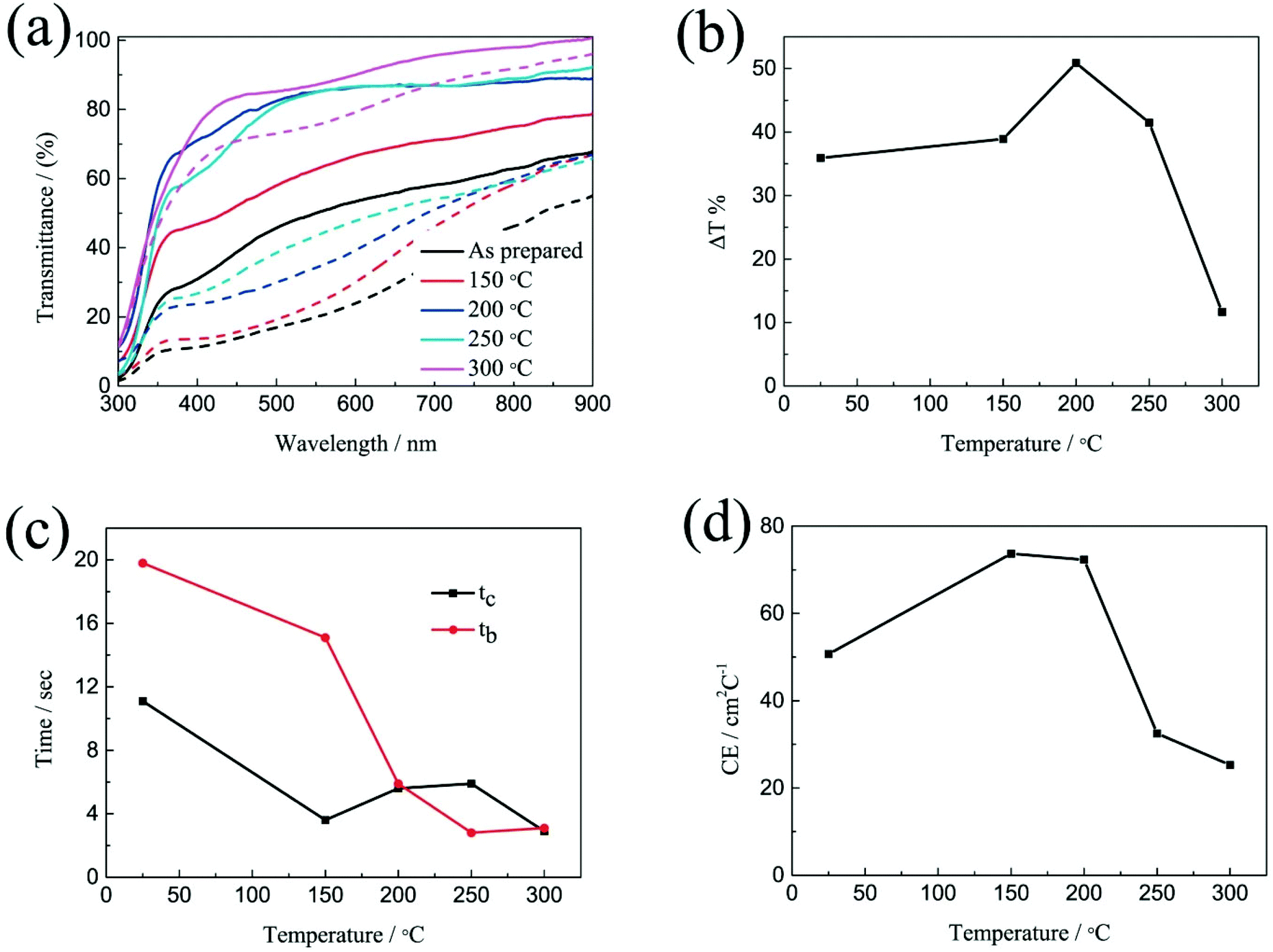 | ||
| Fig. 4 (a) Optical transmittance spectra at colored and bleached states, (b) corresponding to transmittance modulations, (c) coloration time and bleaching time and (d) CE values of the printed NiO films with 6 layers which have undergone annealing at different temperatures. | ||
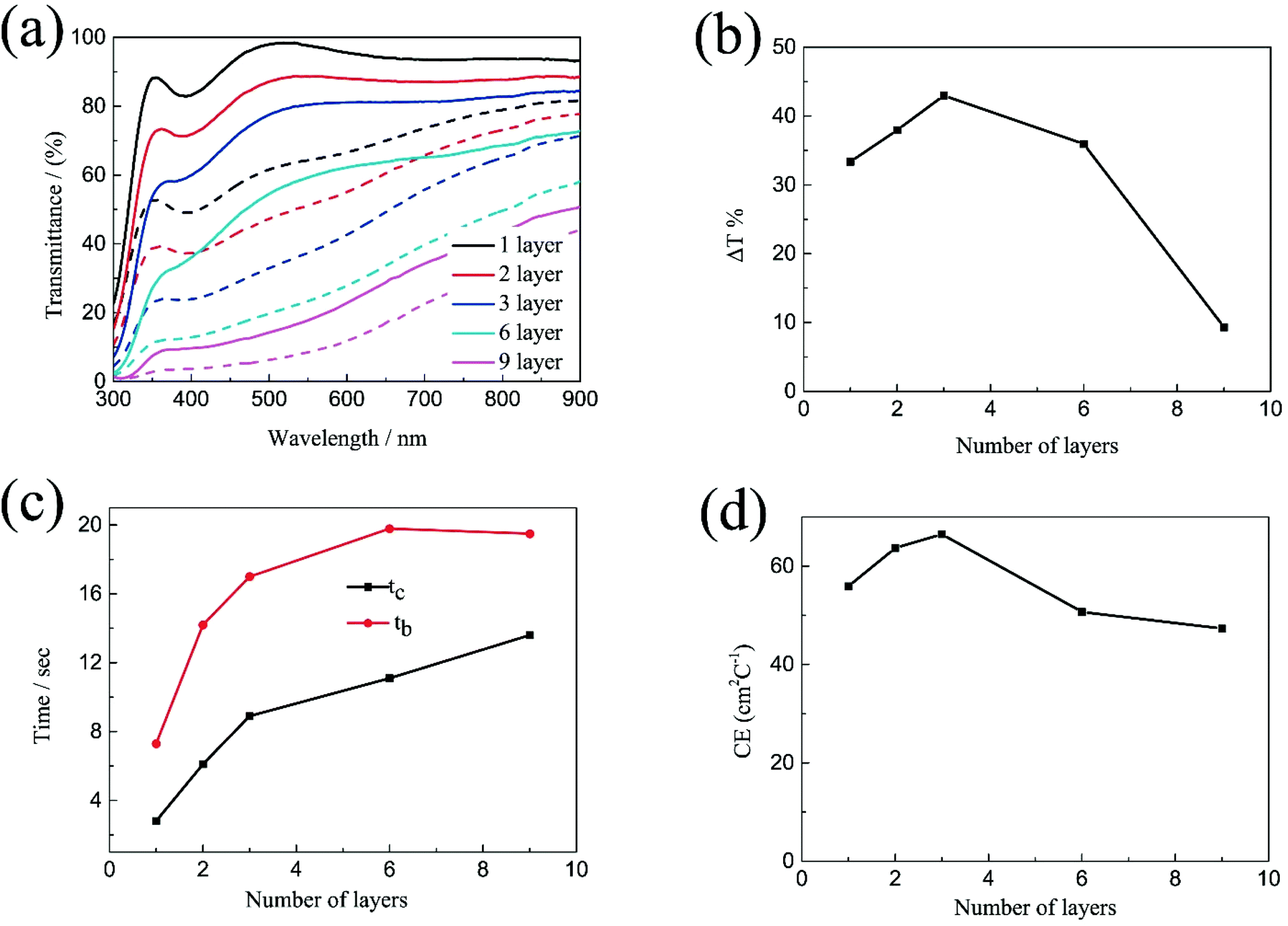
The electrochromic properties of the printed NiO films with different layers which have undergone annealing at 200 °C for 2 h were also further measured in the three-electrode electrochemical cell. It can be seen from Fig. 5a and b that though the transmittance of the NiO films in both the colored and bleached states decrease with increasing the number of NiO layers, the optical modulation of the films increases linearly. This proves that removal of the organic binder helps in facilitating ion diffusion in thick layers. The largest optical modulation of the printed NiO films is 64.2% at 550 nm for the 9 layers. The optical modulation of 64.2% is comparable to that of the NiO film prepared by reactive dc magnetron sputtering (70%),40 electrodeposition41 and hot-filament metal-oxide vapor deposition,42 but much higher than that of the NiO films obtained from pulsed laser deposition (48%)43 and oxidation in air (37%).44 The coloration and bleaching times of the printed NiO films which have undergone annealing at 200 °C for 2 h, as predicted, increase with increasing the number of NiO layers as shown in Fig. 5c and S6,† but faster than that of the corresponding unannealed NiO films. In general, the bleaching time is shorter than that of the coloration time. The CE increases with increasing the number of NiO layers (Fig. 5d). The CE value of the printed film with 9 NiO layers is 136.7 cm2 C−1, which is comparable to that of the NiO film prepared via a electrodeposition technique (107 cm2 C−1),45 but much higher than that of the NiO films prepared by chemical bath deposition (33.9 cm2 C−1)46 and aerosol-assisted chemical vapor deposition (45 cm2 C−1).47
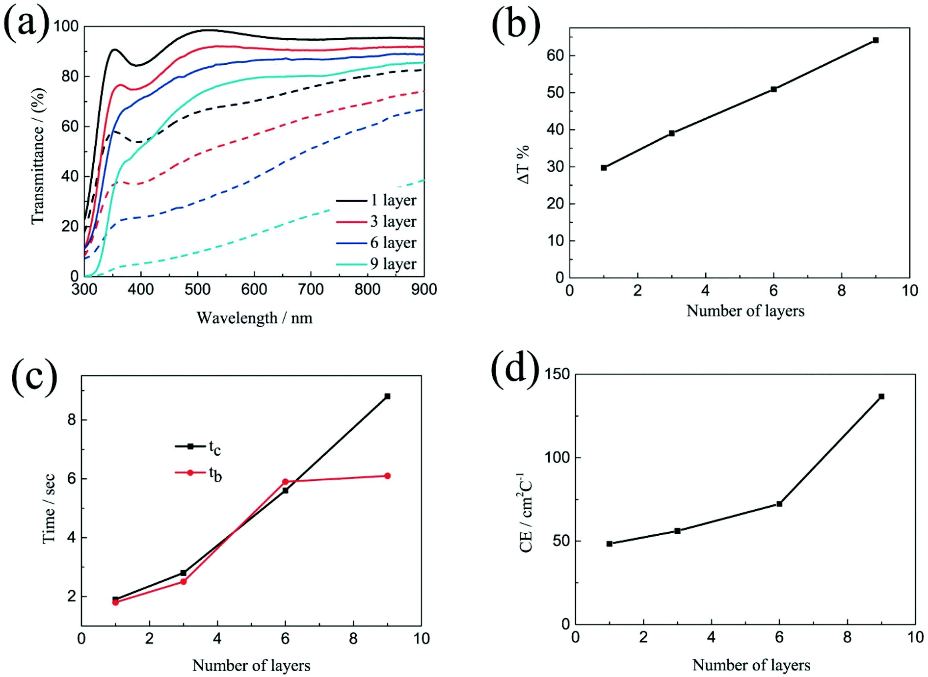 | ||
| Fig. 5 (a) Optical transmittance spectra at colored and bleached states, (b) corresponding to transmittance modulations, (c) coloration time and bleaching time and (d) CE values of the printed NiO films with different layers which have undergone annealing at 200 °C temperature for 2 h. | ||
To evaluate the electrochromic properties of the solid device, the printed NiO films as the ion storage layer, WO3 films as the electrochromic layer, and PMMA-based polymer electrolyte as the solid electrolyte were assembled with the configuration as shown in Fig. 6a. Before assembling into electrochromic devices, both printed NiO and WO3 films were annealed at 200 °C for 2 h. The thickness of the NiO and WO3 films is 450 and 635 nm, respectively, as shown in Fig. S7.† For comparison, a solid device without an NiO film was also prepared with the same WO3 film and electrolyte, just replacing the NiO film by a piece of bare ITO glass. The transmittance spectra of the solid electrochromic devices in the colored and bleached states were measured at −2.5 and 2.5 V for 30 s, respectively. It can be seen from Fig. 6b that the solid device with the NiO film as the ion storage layer showed an optical modulation of 75% at 633 nm, which is much larger than that of the device using the bare ITO complementary electrode without the NiO film (18.8%) and other complementary all solid-state electrochromic devices recently reported.48–50 The digital photos of the solid device with the NiO film as the ion storage layer in the bleached state and the colored state are shown in the inset of Fig. 6b and a pattern device in the colored state and the bleached state are shown in Fig. 6c. The switching speed characteristics of the solid electrochromic devices were studied by employing CA and the corresponding in situ transmittance at 633 nm, as shown in Fig. S8a.† The coloration and bleaching times of the solid device with the NiO film as the ion storage layer is 10.0 and 13.1 s, respectively, which is longer than that of the solid device without the NiO film (12.5 and 5.9 s, respectively), but it is shorter than that of the complementary all solid-state electrochromic device previously reported (10.0 and 20 s, respectively).51 In addition, the CE can be calculated from the curve slope of the ΔOD at a wavelength of 633 nm vs. the inserted charge density in the colored state as shown in Fig. 6d. The CE of the solid device with the NiO film as the ion storage layer is 131.9 cm2 C−1, which is more than 2 times larger than that of the solid device without the NiO film. Fig. S8b† shows the first 100 coloration-bleaching cycles, which vary as a function of time within 6000 s for the solid electrochromic devices. The solid device with the NiO film as an ion storage layer sustains a transmittance modulation of about 81.1% of the corresponding initial values after 100 coloration-bleaching cycles. However, the solid device without the NiO film only maintains a transmittance modulation of about 65.9% of its initial value after 100 cycles. Therefore, the results verify that the solid device with the NiO film as the ion storage layer exhibits more stable and reversible electrochromic performance. The enhancement of electrochromic performances is attributed to the synergistic contribution from NiO and WO3 films, because the NiO film not only performs as an ion storage layer, but also as a complementary electrochromic layer in this case.
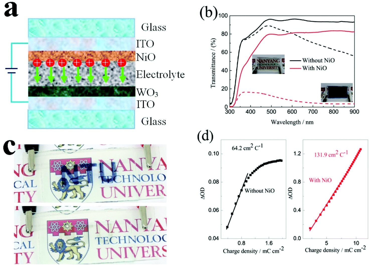 | ||
| Fig. 6 (a) Setup of the solid electrochromic device with NiO as an ion storage layer, (b) transmittance spectra of the solid electrochromic device with and without NiO as an ion storage layer in the bleached (2.5 V) and colored (−2.5) states in the wave length range of 300–900 nm (the digital photos of the solid electrochromic device with NiO as an ion storage layer in the bleached state and the colored state are presented in the inset), (c) a photograph of the solid device pattern with NiO as an ion storage layer in the bleached state and the colored state, and (d) the variation of the in situ optical density (ΔOD) vs. the charge density for the solid electrochromic device with and without NiO as an ion storage layer. | ||
4. Conclusions
In summary, a versatile ink formulation was developed to prepare NiO and WO3 inks simultaneously for inkjet printing application. The printed films have strong adhesion with an ITO glass. The number of printed layers and the annealed temperature could be selectively chosen to prepare electrochromic films with the desired performance. The printed NiO with 9 layers which have undergone annealing at 200 °C for 2 h exhibits an optical modulation of 64.2% and a CE of 136.7 cm2 C−1. In addition, an all solid device was assembled with a printed NiO film as an ion storage layer, a printed WO3 film as an electrochromic layer, a PMMA-based polymer electrolyte as a solid electrolyte which shows a larger optical modulation, a higher CE and more stable cycling performance than that of the solid device without the NiO film. The enhancement of electrochromic performance is attributed to the synergistic contribution from the NiO and WO3 films, because the NiO film not only performs as an ion storage layer, but also as a complementary electrochromic layer.Acknowledgements
This research was supported by the A*Star-MND Green Building Joint Grant 1321760013. A part of the work is also supported by NTU-HUJ-BGU Nanomaterials for Energy and Water Management Programme under the Campus for Research Excellence and Technological Enterprise (CREATE) and the National Research Foundation Competitive Research Programme, Award no. NRF-CRP-13-2014-02, that is supported by the National Research Foundation, Prime Minister's Office, Singapore.References
- A. Llordes, G. Garcia, J. Gazquez and D. J. Milliron, Nature, 2013, 500, 323–326 CrossRef CAS PubMed.
- X. Xie, K. Kretschmer and G. Wang, Nanoscale, 2015, 7, 13278–13292 RSC.
- S. Vankova, S. Zanarini, J. Amici, F. Camara, R. Arletti, S. Bodoardo and N. Penazzi, Nanoscale, 2015, 7, 7174–7177 RSC.
- G. A. Niklasson and C. G. Granqvist, J. Mater. Chem., 2007, 17, 127–156 RSC.
- H. Jiang, D. Y. Ren, H. F. Wang, Y. J. Hu, S. J. Guo, H. Y. Yuan, P. J. Hu, L. Zhang and C. Z. Li, Adv. Mater., 2015, 27, 3687–3695 CrossRef CAS PubMed.
- H. Jiang, Y. J. Hu, S. J. Guo, C. Y. Yan, P. S. Lee and C. Z. Li, ACS Nano, 2014, 8, 6038–6046 CrossRef CAS PubMed.
- C.-G. Granqvist, Nat. Mater., 2006, 5, 89–90 CrossRef CAS PubMed.
- M. Q. Cui, W. S. Ng, X. Wang, P. Darmawan and P. S. Lee, Adv. Funct. Mater., 2015, 25, 401–408 CrossRef CAS.
- X. H. Yang, G. Zhu, S. H. Wang, R. Zhang, L. Lin, W. Z. Wu and Z. L. Wang, Energy Environ. Sci., 2012, 5, 9462–9466 CAS.
- M. Gratzel, Nature, 2001, 409, 575–576 CrossRef CAS PubMed.
- C. G. Granqvist, Sol. Energy Mater. Sol. Cells, 2000, 60, 201–262 CrossRef CAS.
- C. Y. Yan, W. B. Kang, J. X. Wang, M. Q. Cui, X. Wang, C. Y. Foo, K. J. Chee and P. S. Lee, ACS Nano, 2013, 8, 316–322 CrossRef PubMed.
- X. Liu, A. Zhou, Y. Dou, T. Pan, M. Shao, J. Han and M. Wei, Nanoscale, 2015, 7, 17088–17095 RSC.
- G. F. Cai, J. P. Tu, J. Zhang, Y. J. Mai, Y. Lu, C. D. Gu and X. L. Wang, Nanoscale, 2012, 4, 5724–5730 RSC.
- F. Lin, D. Nordlund, T.-C. Weng, R. G. Moore, D. T. Gillaspie, A. C. Dillon, R. M. Richards and C. Engtrakul, ACS Appl. Mater. Interfaces, 2012, 5, 301–309 Search PubMed.
- S. H. Baeck, K. S. Choi, T. F. Jaramillo, G. D. Stucky and E. W. McFarland, Adv. Mater., 2003, 15, 1269–1273 CrossRef CAS.
- Y. Zhou, D. H. Gu, Y. Y. Geng and F. X. Gan, Mater. Sci. Eng., B, 2006, 135, 125–128 CrossRef CAS.
- A. Karuppasamy, Appl. Surf. Sci., 2013, 282, 77–83 CrossRef CAS.
- M. S. Wu and C. H. Yang, Appl. Phys. Lett., 2007, 91, 033109 CrossRef.
- E. Khoo, P. S. Lee and J. Ma, J. Eur. Ceram. Soc., 2010, 30, 1139–1144 CrossRef CAS.
- F. Cao, G. X. Pan, X. H. Xia, P. S. Tang and H. F. Chen, Electrochim. Acta, 2013, 111, 86–91 CrossRef CAS.
- J. Zhang, J. P. Tu, X. H. Xia, X. L. Wang and C. D. Gu, J. Mater. Chem., 2011, 21, 5492–5498 RSC.
- J.-S. Yu, I. Kim, J.-S. Kim, J. Jo, T. T. Larsen-Olsen, R. R. Sondergaard, M. Hosel, D. Angmo, M. Jorgensen and F. C. Krebs, Nanoscale, 2012, 4, 6032–6040 RSC.
- D. Angmo, T. T. Larsen-Olsen, M. Jørgensen, R. R. Søndergaard and F. C. Krebs, Adv. Energy Mater., 2013, 3, 172–175 CrossRef CAS.
- C.-C. Huang, Z.-K. Kao and Y.-C. Liao, ACS Appl. Mater. Interfaces, 2013, 5, 12954–12959 CAS.
- S. Yuichi, F. Tomoaki and A. Masatoshi, Jpn. J. Appl. Phys., 2008, 47, 7630–7634 CrossRef.
- M. Layani, P. Darmawan, W. L. Foo, L. Liu, A. Kamyshny, D. Mandler, S. Magdassi and P. S. Lee, Nanoscale, 2014, 6, 4572–4576 RSC.
- C. Costa, C. Pinheiro, I. Henriques and C. A. T. Laia, ACS Appl. Mater. Interfaces, 2012, 4, 5266–5275 CAS.
- C. Costa, C. Pinheiro, I. Henriques and C. A. T. Laia, ACS Appl. Mater. Interfaces, 2012, 4, 1330–1340 CAS.
- G. H. Shim, M. G. Han, J. C. Sharp-Norton, S. E. Creager and S. H. Foulger, J. Mater. Chem., 2008, 18, 594–601 RSC.
- P. J. Wojcik, L. Santos, L. Pereira, R. Martins and E. Fortunato, Nanoscale, 2015, 7, 1696–1708 RSC.
- G. F. Cai, X. Wang, M. Q. Cui, P. Darmawan, J. X. Wang, A. L.-S. Eh and P. S. Lee, Nano Energy, 2015, 12, 258–267 CrossRef CAS.
- X. Sun, G. Wang, J.-Y. Hwang and J. Lian, J. Mater. Chem., 2011, 21, 16581–16588 RSC.
- S. Y. Han, D. H. Lee, Y. J. Chang, S. O. Ryu, T. J. Lee and C. H. Chang, J. Electrochem. Soc., 2006, 153, C382–C386 CrossRef CAS.
- K. Fominykh, J. M. Feckl, J. Sicklinger, M. Döblinger, S. Böcklein, J. Ziegler, L. Peter, J. Rathousky, E.-W. Scheidt, T. Bein and D. Fattakhova-Rohlfing, Adv. Funct. Mater., 2014, 24, 3123–3129 CrossRef CAS.
- A. Benoit, I. Paramasivam, Y. C. Nah, P. Roy and P. Schmuki, Electrochem. Commun., 2009, 11, 728–732 CrossRef CAS.
- G. F. Cai, D. Zhou, Q. Q. Xiong, J. H. Zhang, X. L. Wang, C. D. Gu and J. P. Tu, Sol. Energy Mater. Sol. Cells, 2013, 117, 231–238 CrossRef CAS.
- X. H. Xia, J. P. Tu, J. Zhang, X. L. Wang, W. K. Zhang and H. Huang, Sol. Energy Mater. Sol. Cells, 2008, 92, 628–633 CrossRef CAS.
- R. Cerc Korošec, P. Bukovec, B. Pihlar and J. Padežnik Gomilšek, Thermochim. Acta, 2003, 402, 57–67 CrossRef.
- R.-T. Wen, G. A. Niklasson and C. G. Granqvist, Thin Solid Films, 2014, 565, 128–135 CrossRef CAS.
- G. F. Cai, J. P. Tu, C. D. Gu, J. H. Zhang, J. Chen, D. Zhou, S. J. Shi and X. L. Wang, J. Mater. Chem. A, 2013, 1, 4286–4292 CAS.
- R. A. Patil, R. S. Devan, J.-H. Lin, Y.-R. Ma, P. S. Patil and Y. Liou, Sol. Energy Mater. Sol. Cells, 2013, 112, 91–96 CrossRef CAS.
- I. Bouessaya, A. Rougier, P. Poizot, J. Moscovici, A. Michalowicz and J. M. Tarascon, Electrochim. Acta, 2005, 50, 3737–3745 CrossRef.
- G. F. Cai, C. D. Gu, J. Zhang, P. C. Liu, X. L. Wang, Y. H. You and J. P. Tu, Electrochim. Acta, 2013, 87, 341–347 CrossRef CAS.
- A. C. Sonavane, A. I. Inamdar, P. S. Shinde, H. P. Deshmukh, R. S. Patil and P. S. Patil, J. Alloys Compd., 2010, 489, 667–673 CrossRef CAS.
- G. F. Cai, J. P. Tu, D. Zhou, L. Li, J. H. Zhang, X. L. Wang and C. D. Gu, J. Phys. Chem. C, 2014, 118, 6690–6696 CAS.
- M. Z. Sialvi, R. J. Mortimer, G. D. Wilcox, A. M. Teridi, T. S. Varley, K. G. U. Wijayantha and C. A. Kirk, ACS Appl. Mater. Interfaces, 2013, 5, 5675–5682 CAS.
- R. Ramadan, H. Kamal, H. M. Hashem and K. Abdel-Hady, Sol. Energy Mater. Sol. Cells, 2014, 127, 147–156 CrossRef CAS.
- C.-C. Jaing, C.-J. Tang, C.-C. Chan, K.-H. Lee, C.-C. Kuo, H.-C. Chen and C.-C. Lee, Appl. Opt., 2014, 53, A154–A158 CrossRef CAS PubMed.
- K. J. Patel, M. S. Desai and C. J. Panchal, J. Solid State Electrochem., 2015, 19, 275–279 CrossRef CAS.
- J. Zhang, J. P. Tu, X. H. Xia, Y. Qiao and Y. Lu, Sol. Energy Mater. Sol. Cells, 2009, 93, 1840–1845 CrossRef CAS.
Footnote |
| † Electronic supplementary information (ESI) available. See DOI: 10.1039/c5nr06995e |
| This journal is © The Royal Society of Chemistry 2016 |