
Resonant energy transfer between patterned InGaN/GaN quantum wells and CdSe/ZnS quantum dots
Xingsheng
Xu
* and
Huayong
Wang
State Key Laboratory of Integrated Optoelectronics, Institute of Semiconductors, Chinese Academy of Sciences, Beijing 100083, China. E-mail: xsxu@semi.ac.cn
First published on 27th November 2015
Abstract
We explore an easy method for preparation of a hybrid device of a photonic crystal InGaN/GaN quantum well (QW) and colloidal quantum dots using conventional photolithography. It is demonstrated from electroluminescence spectra that Förster resonance energy transfer takes place efficiently between the photonic crystal InGaN/GaN QW and CdSe/ZnS colloidal quantum dots. From the photoluminescence decay of the InGaN/GaN QW, the largest Förster resonance energy transfer efficiency between the photonic crystal GaN quantum well and colloidal quantum dots is measured as 88% and the corresponding Förster-resonance-energy-transfer fraction reached 42%. An easy approach is explored to realize a highly efficient electrically driven colloidal quantum dot device using the Förster-resonance-energy-transfer mechanism.
Introduction
Semiconductor colloidal quantum dots (CQDs) synthesized by wet chemical methods exhibit advantages1 of low cost, high quantum efficiency, room-temperature operation and suitability for solution processes. These advantages mean that CQDs have a broad range of potential applications in optoelectronic devices, such as photodetectors,2 light-emitting diodes (LEDs),3 lasers,4 photovoltaic devices5etc. The capping layer and shell of a core–shell CQD can protect the core, enhance the emission efficiency and decrease the blinking effect.6 However, CQDs show low conductivity due to an insulating organic capping layer on nanocrystals,7 which makes it difficult to realize an efficient electrically driven device directly, especially LEDs or lasers. To overcome this difficulty, combining CQDs with a semiconductor quantum well (QW) to realize an electrically driven device through radiative energy transfer8 or non-radiative energy transfer is an effective approach.9–11 Förster resonance energy transfer (FRET) is an energy transfer mechanism through dipole–dipole interactions where energy is non-radiatively transferred from a donor to an acceptor.12 Non-radiative transfer means that the donor will not give out emission during the energy transfer process. FRET occurs on conditions that the donor is close enough to the acceptor, such that the electron in the excited state of the donor can transfer to the excited state of the acceptor before it decays to the donor's ground state. Through dipole–dipole interactions, energy from the donor is transferred to the acceptor.Combining a GaN LED with CQDs could greatly improve the optoelectronic properties of CQDs. Achermann et al. reported FRET between a GaN QW and CdSe CQDs,13 where the distance between CdSe CQDs and InGaN/GaN QW was only 3 nm. Under optical pumping, a FRET efficiency of 55% was obtained from this structure.13 Chanyawadee et al. introduced CQDs adjacent to the QW active area of a GaN LED through etched slot holes. In this case, the electrically excited carrier in the LED could transfer to the adjacent CQDs by FRET. It was found that 18% of electron–hole pairs were generated in the FRET process, and the FRET efficiency reached 82%.11 Here, we investigate the FRET between a photonic crystal (PhC) GaN LED and CQDs. The PhC was fabricated by conventional semiconductor processes including photolithography, inductively coupled plasma etching and deposition of electrodes. By measuring the LED P–I characteristics, it was found that the GaN LED with a PhC hole etched to the GaN QW layer showed a power enhancement compared with the structure without PhC. Using the drop-casting method, the CQDs were introduced into the holes of the PhC GaN LED. By comparing electroluminescence (EL) spectra and photoluminescence (PL) decay processes of the hybrid device of PhC GaN LED and CQDs with that without PhC, it was demonstrated that the FRET occurred between the GaN QW and CQDs.
Experimental
Fabrication of the photonic crystal InGaN/GaN light-emitting-diode with colloidal quantum dots
The InGaN/GaN QW material was deposited on a sapphire substrate by a metal–organic chemical vapor deposition method, including 3 μm thick n-GaN, then five pairs of GaN/InGaN QWs, on which a p-GaN with a thickness of 200 nm was deposited. PhCs with lattice constants larger than 1 μm were fabricated on the GaN LED using a conventional photolithography method. Firstly, a thin layer of ITO was deposited on P-GaN. The photoresist was spun on the ITO layer, and then the PhC pattern was defined on the resist by photolithography. The PhC pattern was transferred from the photoresist to the ITO layer by wet-etching, and then etched into p-GaN and InGaN/GaN QW by inductively coupled plasma dry etching. The average hole etching depth was 225 nm (Fig. 1(b)), which reached the InGaN/GaN QW layer. After PhC GaN LED fabrication, CQDs with a center emitting wavelength of 585 nm were drop-cast on the surface of the PhC GaN LED. The core–shell CdSe/ZnS CQDs were synthesized by a wet-chemical method. With a center emitting wavelength of 585 nm, the CdSe core thickness is approximately 4.0 nm, the ZnS shell thickness is approximately 1.6 nm and a trioctylphosphine oxide capping ligand thickness is 2–3 nm. EL spectra were recorded with a home-built micro-area spectrum system. An Agilent pulse voltage source was used as an electrically driven source. In EL spectral measurements, the voltage pulse duty cycle was 50%. In the PL decay experiments, a 400 nm pulse laser diode with a pulse width of 65 ps was used as a pump light. A 40×/0.60 objective was used as focus lens and collection lens. The collected signal was sent to a silicon avalanche photodiode (APD) and a time-correlated-single-photon-counting (TCSPC) system for lifetime analysis.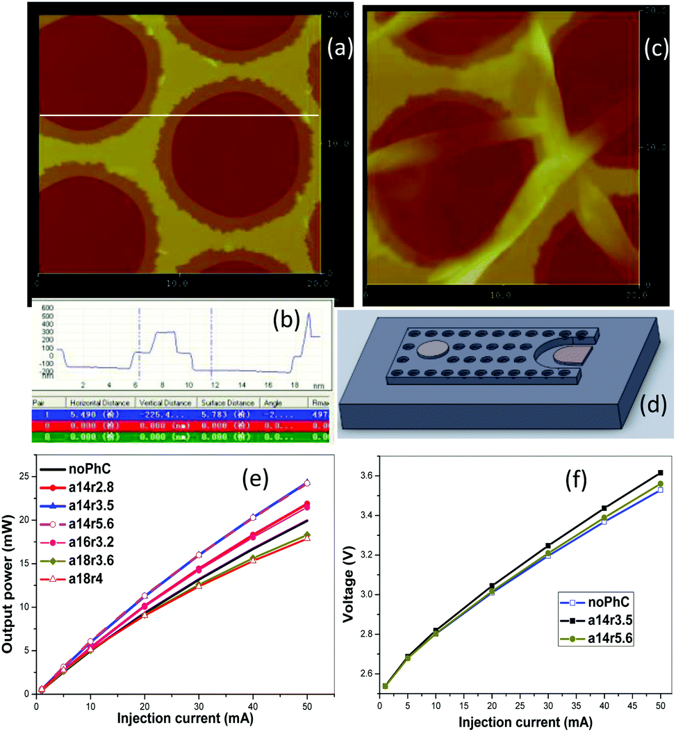 | ||
| Fig. 1 (a) Atomic force microscopy image of fabricated PhC on p-GaN, where the green top layer is ITO. (b) Line scan of cross-section of the structure in (a) along the white line; hole depth of GaN layer is 225.4 nm (shown by “vertical distance”). (c) AFM images of PhC-GaN LED with CQDs. (d) Schematic structure of a PhC GaN LED. The chip size of the GaN LED is 254 μm × 584 μm. (e) P–I curves for GaN LED with and without PhCs, where a represents the lattice constant and r hole radius, the symbol of noPhC represents GaN LED without PhCs, a14r3.5 represents the GaN LED with PhC with a lattice constant of 14 μm and a radius of 3.5 μm, etc. (f) I–V curves for GaN LED with and without PhCs. | ||
Characterization of the photonic crystal InGaN/GaN light-emitting-diode
The CQDs with a center emitting wavelength of 585 nm and a concentration of 1.6 μM were drop-cast onto the GaN LED. The atomic force microscopy (AFM) images of PhC GaN LED and that with CQDs are shown in Fig. 1(a)–(c), and the structure of PhC GaN LED is schematically shown in Fig. 1(d). From the analysis of the cross-section in Fig. 1(b) of the structure in Fig. 1(a) along the white line, the hole depth of the GaN layer is 225.4 nm (shown by the “vertical distance”). From the AFM image in Fig. 1(c), though the CQDs have not filled the whole holes, but they covered partly the bottom surface of the holes and touched the InGaN/GaN QW, where FRET can take place between InGaN/GaN QW and CQDs. By comparing the measured P–I curves of the GaN LED with PhCs and that without PhCs in Fig. 1(e), it is found that the extraction efficiency of the GaN LED with PhCs is enhanced. For PhC with a lattice constant of 14 μm, a hole radius of 3.5 μm and a depth of 225 nm, under a driving current of 50 mA, the output power is enhanced by more than 20% compared with the GaN LED without PhCs. The I–V characteristics measured for GaN LED with and without PhCs are shown in Fig. 1(f), where the hollow-square line is the I–V curve for the GaN LED without PhC, the solid-square line is for the GaN LED with PhC with a lattice constant of 14 μm and a diameter of 7 μm, and the solid-circle line between the above two is for PhC-LED with a lattice constant of 14 μm and a diameter of 11.2 μm. It can be found that, at the same injection current, the driving voltage for the GaN LED with PhCs is higher than that without PhCs.Results and discussion
Energy transfer between InGaN/GaN QW and CdSe/ZnS QD studied by EL spectra
CdSe/ZnS CQDs were drop-cast on the GaN LED with PhCs, and the quantum yield of the CQDs is approximately 50%. From Fig. 2(a), it is seen that the absorption spectrum of CdSe/ZnS QDs is broad and covers the emission spectrum of the InGaN/GaN QW, and the EL spectrum of the InGaN/GaN QW is sufficiently separated from that of CdSe/ZnS QDs. The central emission wavelength of the spectrum of CdSe/ZnS QD is 585 nm, and full width at half-maximum is 32 nm. After the CdSe/ZnS QDs are introduced into the PhC holes, the distance between CQDs and QW is close enough for FRET to occur. The spectra of InGaN/GaN QW and CdSe/ZnS QDs with a concentration 1.6 μM with PhCs and without PhCs under a driving voltage of 3.6 V are shown in Fig. 2(b), where the spectra were recorded at electrically-driving time of 10–50 minutes and the EL intensities of the InGaN/GaN QW are normalized. It is seen from Fig. 2(b) that the intensities and the center wavelengths of spectra of CQDs on PhCs change with the radius of the PhC hole and differ from those without PhCs. There may be two reasons for this: one is that the spectra of CQDs on PhCs are modified by the leaky modes of the PhC slab;14 another is that the spectra change with energy transfer. The color-conversion ratio is defined as the ratio of the CQD emission intensity in the hybrid structure to the same InGaN/GaN QW emission intensity. The color-conversion ratio can approximately represent the color-conversion efficiency, which is defined as the ratio of the CQD emission intensity in the hybrid structure to the intensity of the InGaN/GaN QW absent CQD.11 For CQDs on PhC with a lattice constant of 14 μm and a radius of 3.5 μm measured at 10–50 minutes, the peak color-conversion ratio is 17.5%, while it is 13.5% for PhC with a radius of 5.6 μm. For the CQDs on the GaN LED without PhC, the color-conversion ratio reaches 12.2%, where the energy transfer is mainly radiative energy transfer, while the energy transfer for the GaN LED with PhC includes radiative energy transfer and non-radiative energy transfer (FRET). The color-conversion efficiency for a larger hole of the radius of 5.6 μm is smaller than that of the radius of 3.5 μm, which is due to that the color-conversion efficiency also depends on the coupling of the emission to the leaky mode of the PhC slab. With different color-conversion ratios, the center wavelength and the asymmetry of spectra of the QW are different. Under a driving voltage of 3.6 V, the energy transfer between the QWs and the CQDs was studied as a function of electrically driving time, and corresponding EL spectra are shown in Fig. 2(c), where the CdSe/ZnS CQDs have a concentration of 8 μM. After the QW spectra and the QD spectra are fitted to a Gaussian function, the spectral parameters are shown in Fig. 2(d) and (e). It should be mentioned that the QW spectra did not fit well to a single Gaussian function but they can be fitted well to a bi-Gaussian function. The spectral center wavelength of GaN QW shows a decreasing trend with increasing electrically-driving time, while the spectral width shows an almost opposite variation trend to that of the spectral center wavelength. However, both the center wavelength and the spectral width of CQD spectra decrease with electrically-driving time. It means that the spectra of CdSe QDs shift to blue with increasing electrically-driving time. The PhC used here has the same parameters of the lattice constant of 14 μm and the hole radius of 3.5 μm as the PhC GaN LED used in Fig. 1(e) that shows enhanced extraction efficiency. The color-conversion ratios under different electrically-driving time are shown in Fig. 2(f). The color-conversion ratio at 5 minutes is 41.8%. In the time range 10–50 minutes, the color-conversion ratios are around 23%. The average color-conversion ratio in the time range of 5–50 minutes is 25.5%. These color-conversion ratios of the hybrid device with PhC are much higher than that without PhC (12% measured in the time range 10–50 minutes). It indicates that FRET takes place between GaN QW and CQDs with PhC.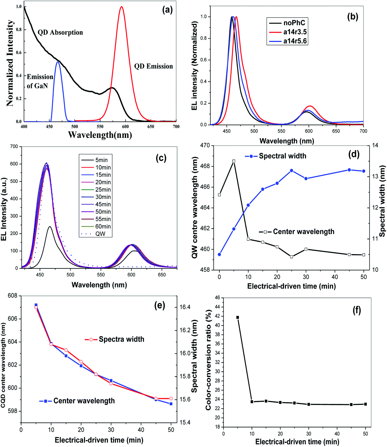 | ||
| Fig. 2 (a) The absorption (black line) and emission (red line) spectra of CdSe/ZnS QDs and electroluminescence emission spectrum of GaN LED (blue line). (b) Comparison of the energy transfer for a structure with PhCs of different parameters and that without PhCs. (c) Spectra of QW and CQDs on PhC with a lattice constant of 14 μm and a radius of 3.5 μm under different electrically driving time. Where the symbol of QW represents the GaN QW without PhC. (d) Center wavelength and spectral width of QW spectra. (e) Center wavelength and spectral width of CQD spectra. (f) Color-conversion efficiencies under different electrically-driving time. | ||
The spectra of the hybrid LED consisting of InGaN/GaN QW and CdSe/ZnS QDs with various concentrations were recorded and analyzed under an electrically-driving time of approximately 15 minutes. The color-conversion ratios were calculated from the spectra. It was found that the color-conversion ratio, and the center wavelengths of QWs and CQDs spectral width vary with CQD concentration, which is mainly due to energy transfer between CQDs and QW because the variation tendency of the center wavelength of QW spectra with CQD concentration is in accord with that of the color-conversion ratio. Moreover, through simulation, the refractive index variation of the CQD film may have a weak effect on the EL intensity and the QW spectral shape.
FRET between InGaN/GaN QW and CdSe/ZnS CQD studied by PL decay processes
To determine how many electron–hole pairs take part in FRET and the FRET efficiency, the PL decay processes were measured. From the above discussion, a PhC with a lattice constant of 14 μm and a radius of 3.5 μm is suitable for the experiment. After studying the color-conversion ratio (efficiency) with CQDs of various concentrations, it was found that the energy transfer efficiency was pronounced at a concentration of 1.6 μM. In the decay process experiment described in the following, CQDs with a concentration of 1.6 μM were drop-cast on a PhC with a lattice constant of 14 μm and a radius of 3.5 μm. The PL decay processes from the InGaN/GaN QW were measured by a silicon APD detector and analyzed by a TCSPC system. The measurement results are shown in Fig. 3, where the blue line represents the decay process from InGaN/GaN QW with CQDs without PhCs, the black line represents that from InGaN/GaN QW without PhCs and CQDs, the red line is that from InGaN/GaN QW with PhCs without CQDs and the purple line is that from InGaN/GaN QW with PhCs with CQDs. As these curves are normalized, it can be seen that the decay rates are largely different from each other. The PL decay from InGaN/GaN QW with CQDs with PhCs is faster than those from the others, especially faster than that from InGaN/GaN QW with CQDs without PhCs. This indicates that FRET takes place in the GaN LED with PhCs with CQDs. To demonstrate this, the decay process is fitted to a bi-exponential as11| IHQW(t) = Ae−kQWt + Be−(kQW+kET)t | (1) |
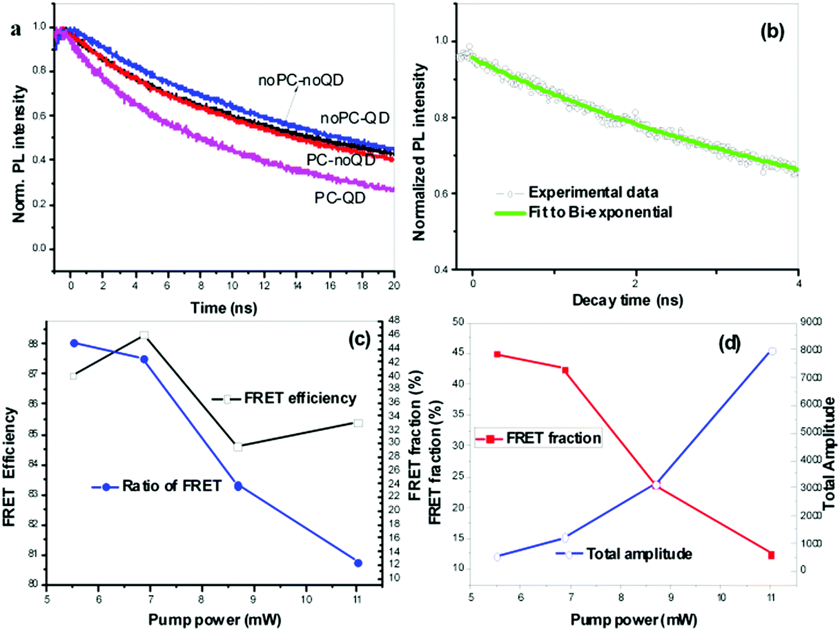 | ||
| Fig. 3 PL decay process of InGaN/GaN QW. (a) PL decay processes of InGaN/GaN QW: black line, InGaN/GaN QW without PhCs without CQDs; blue line, InGaN/GaN QW with CQDs without PhCs; red line, InGaN/GaN QW with PhCs without CQDs; purple line, InGaN/GaN QW with PhCs with CQDs. (b) PL decay curves of InGaN/GaN QW with PhCs with CQDs fitted to bi-exponential: gray line, experimental data; green line, fitting result. (c) The decay process and the FRET efficiency for hybrid PhC InGaN/GaN QW with CdSe QDs under various excitation powers. FRET efficiencies and FRET fraction under various excitation powers (before the objective). (d) The total amplitude from bi-exponential fitting to PL decay processes under various excitation powers. The CQD concentration is 1.6 μM. | ||
where kQW is the emission decay rate of InGaN/GaN QW with PhC, kET is the non-radiative energy transfer rate, and A and B are the amplitudes. Parameters kET, kQW, A and B can be obtained by fitting the decay process of InGaN/GaN QW with PhCs with CQDs to eqn (1). The first 4 ns of the decay curve of InGaN/GaN QW with PhCs and CQDs can be fitted to eqn (1), which is similar to the case in ref. 11, 15; whereas, in the same decay time range, the decay curves of InGaN/GaN QW with PhCs without CQDs and that without PhCs and CQDs cannot be fitted to a bi-exponential like eqn (1). In the long decay time range, such as from 20 ns to 30 ns, the decay curve of InGaN/GaN QW with PhCs without CQDs can also be fitted to a bi-exponential (not shown), which is due to the modification of the fluorescence from PhC. To remove the effect of PhC on the FRET, we study the time range of 0–4 ns where PhC almost has no effect on the lifetime.16 After the decay curve from InGaN/GaN QW with PhCs with CQDs is fitted to eqn (1), the parameters are obtained as: A = 0.7429, B = 0.2136, kQW = 0.0520 ns−1, kET + kQW = 0.3136 ns−1, kET = 0.2616 ns−1, the FRET fraction is
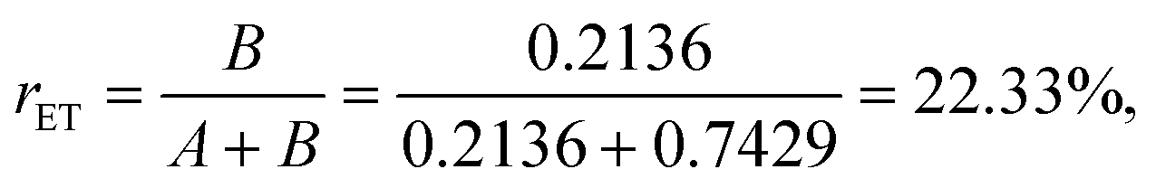
and the FRET efficiency is
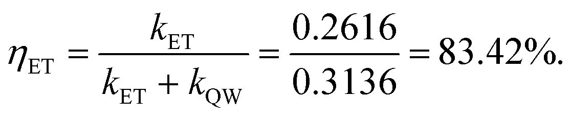
In the experiment, it was found that the FRET efficiency varies with the excitation power; however, in the excitation power range we used, the FRET efficiency does not vary linearly with the excitation power. From Fig. 3(c) and (d), the largest FRET efficiency reaches 88% at an excitation power of 6.82 mW, and the lowest FRET efficiency is 84.59% at an excitation power of 8.69 mW. It is seen that in the excitation power range we used, all the FRET efficiencies are higher than 84%. The FRET fraction changes much with excitation power, and it decreases almost linearly with increasing excitation power. The largest FRET fraction is 44% under the lowest excitation power of 5.5 mW, but at the largest excitation power of 11 mW, the FRET fraction decreases to 12%. On the other hand, the PL intensity of InGaN/GaN QW increases with increasing excitation power, whereas the FRET fraction decreases. This means that the increased excitation power mainly contributes to the InGaN/GaN QW emission, and the ratio of electron–hole pairs undergoing FRET to the total amount of generated electron–hole pairs decreases with increasing excitation power. As mentioned above, under appropriate excitation power, such as 6.8 mW, the FRET fraction is 42.4% and the FRET efficiency is 88%. In the experiment, we tried to focus the pump light at the interface between the QW and the CQDs. Under relatively low excitation power, the pump light mainly excites the QW and then transfers energy to CQDs. Due to the holes of the PhC being much larger than the holes used in previous work,11 a larger fraction of acceptors can be close to donors; therefore, the FRET fraction and efficiency are higher here. In our case, the size of the CdSe/ZnS QDs (ligand molecule thickness of 2–3 nm) is a little larger than that used previously (ligand molecule thickness of 2 nm),11 due to the size of PhC holes being much larger in our case, and then the non-radiative losses of the QW from surface recombination are smaller.17 Therefore, the efficiency of the non-radiative energy transfer (FRET) is higher than that obtained previously.11
Conclusions
In conclusion, a PhC GaN LED structure was designed and fabricated by a conventional photolithography and dry etching method. After CQDs were introduced into the PhC holes of the GaN LED, the EL spectra and the PL decay processes were studied. It was found that FRET took place between the InGaN/GaN QW and the CdSe/ZnS QDs by both electrical driving and optical pump. The color-conversion efficiency was studied under the different conditions of electrically driving time and pump powers. The high FRET fraction of electron–hole pairs was 42% and the FRET efficiency reached 88%. This FRET efficiency and FRET fraction are the highest ones obtained to date between InGaN/GaN QW and CdSe/ZnS QDs. We present an easy method for fabricating a device showing FRET between an electrically driven GaN LED and CQDs by conventional photolithography, which is a good way for realizing an effective electrically driven CQD device.Acknowledgements
We acknowledge financial support from the National Basic Research Program under Grant No. 2013CB632105, and the National Natural Science Foundation of China under Grant Nos 61275045 and 61575191.Notes and references
- J. Y. Kim, O. Voznyy, D. Zhitomirsky and E. H. Sargent, Adv. Mater., 2013, 25, 4986 CrossRef CAS PubMed.
- J. P. Clifford, G. Konstantatos, K. W. Johnston, S. Hoogland, L. Levina and E. H. Sargent, Nat. Nanotechnol., 2009, 4, 40 CrossRef CAS PubMed.
- J. Kwak, W. K. Bae, D. Lee, I. Park, J. Lim, M. Park, H. Cho, H. Woo, D. Y. Yoon, K. Char, S. Lee and C. Lee, Nano Lett., 2012, 12, 2362 CrossRef CAS PubMed.
- V. I. Klimov, S. A. Ivanov, J. Nanda, M. Achermann, I. Bezel, J. A. McGuire and A. Piryatinski, Nature, 2007, 447, 441 CrossRef CAS PubMed.
- E. H. Sargent, Nat. Photonics, 2012, 6, 133 CrossRef CAS.
- T. D. Krauss and J. J. Peterson, Nat. Mater., 2012, 11, 14 CrossRef CAS PubMed.
- I. S. Liu, H. H. Lo, C. T. Chien, Y. Y. Lin, C. W. Chen, Y. F. Chen, W. F. Su and S. C. Liou, J. Mater. Chem., 2008, 18, 675 RSC.
- F. S. Diana, A. David, I. Meinel, R. Sharma, C. Weisbuch, S. Nakamura and P. M. Petroff, Nano Lett., 2006, 6, 1116 CrossRef CAS PubMed.
- D. Basko, G. C. La Rocca, F. Bassani and V. M. Agranovich, Eur. Phys. J. B, 1999, 8, 353 CrossRef CAS.
- M. Achermann, M. A. Petruska, D. D. Koleske, M. H. Crawford and V. I. Klimov, Nano Lett., 2006, 6, 1396 CrossRef CAS PubMed.
- S. Chanyawadee, P. G. Lagoudakis, R. T. Harley, M. D. B. Charlton, D. V. Talapin, H. W. Huang and C. Lin, Adv. Mater., 2010, 22, 602 CrossRef CAS PubMed.
- T. Förster, Intermolecular Energy Transfer and Fluorescence, National Research Council of Canada, 1955 Search PubMed.
- M. Achermann, M. A. Petruska, S. Kos, D. L. Smith, D. D. Koleske and V. I. Klimov, Nature, 2004, 429, 642 CrossRef CAS PubMed.
- X. S. Xu, Sci. Rep., 2013, 3, 3228 Search PubMed.
- F. Zhang, J. Liu, G. J. You, C. F. Zhang, S. E. Mohney, M. J. Park, J. S. Kwak, Y. Q. Wang, D. D. Koleske and J. Xu, Opt. Express, 2012, 20, A333 CrossRef CAS PubMed.
- S. Chanyawadee, R. T. Harley, M. Henini, D. V. Talapin and P. G. Lagoudakis, Phys. Rev. Lett., 2009, 102, 077–07402 CrossRef PubMed.
- M. Boroditsky, I. Gontijo, M. Jackson, R. Vrijen, E. Yablonovitch, T. Krauss, C. C. Cheng, A. Scherer, R. Bhat and M. Krames, J. Appl. Phys., 2000, 87, 3497 CrossRef CAS.
| This journal is © The Royal Society of Chemistry 2016 |