
An overview on emerging photoelectrochemical self-powered ultraviolet photodetectors
Jinyuan
Zhou†
 *,
Lulu
Chen†
,
Youqing
Wang†
,
Yongmin
He
,
Xiaojun
Pan
and
Erqing
Xie
*
*,
Lulu
Chen†
,
Youqing
Wang†
,
Yongmin
He
,
Xiaojun
Pan
and
Erqing
Xie
*
School of Physical Science and Technology, Lanzhou University, Lanzhou 730000, Gansu, P.R. China. E-mail: zhoujy@lzu.edu.cn; xieeq@lzu.edu.cn; Fax: +86 931 8915895; Tel: +86 931 8915895
First published on 19th November 2015
Abstract
In recent years, as a new member of ultraviolet photodetectors (UV-PDs), photoelectrochemical UV-PDs (PEC UV-PDs) have received great attention. Compared to conventional photoconductors, PEC UV-PDs exhibit a number of merits, including low cost, environmentally friendly nature, being self-powered, and fast response. This tutorial review provides a comprehensive introduction to this research field, covering from the basics of performance evaluation of PEC UV-PDs, the state-of-the-art advances in structural design, electrolyte matching, and electrode fabrication of PEC UV-PDs, to the integration of multiple functions into a PEC UV-PD. In the end, we present our perspectives on the future development of PEC UV-PDs and highlight the key technical challenges in aiming to stimulate further developments in this research field.
 Jinyuan Zhou | Jinyuan Zhou received his B.S. and Ph.D. degrees in microelectronics and condensed matter physics from Lanzhou University of China in 2002 and 2010, respectively, and then joined Lanzhou University as a lecturer. From 2010 to 2012, he worked at Nanyang Technological University of Singapore as a postdoctoral fellow. In 2013, he was promoted to associate professor. His research interests include semiconductor and carbon nanotube based functional nanomaterials & their applications in energy and optoelectronic devices. |
 Lulu Chen | Lulu Chen received her B.S. degree in physics from Shangqiu Normal University, Henan, China, in 2011. At present, she is a Ph.D. candidate in condensed matter physics under the supervision of Prof. Erqing Xie at Lanzhou University. Her research focused on the synthesis of ZnO and SnO2 nanomaterials and their applications in electrochemical devices, such as dye-sensitized solar cells and self-powered UV-photodetectors. |
 Youqing Wang | Youqing Wang received his B.S. degree in physics from Lanzhou University of China in 2011, and then joined Prof. Erqing Xie's group. At present, he is a Ph.D. candidate in condensed matter physics at Lanzhou University. His research is focused on dye-sensitized solar cells and ultraviolet detectors. |
 Yongmin He | Yongmin He received his Ph.D. degree in condensed matter physics from Lanzhou University of China in 2015. From 2013 to 2015, He was supported by China Scholarship Council to study at Rice University as a visiting student. From 2015 to the present, he worked at Nanyang Technological University of Singapore as a postdoctoral fellow. His current research interests mainly focus on “smart” flexible ECs, and two-dimensional (2D) materials such as graphene, h-BN, transition metal dichalcogenides and their heterostructures. |
 Xiaojun Pan | Xiaojun Pan received his B.S. and Ph.D. degrees in Physics and condensed matter physics from Lanzhou University of China in 2003 and 2008, respectively, and then joined Lanzhou University as a lecturer. From 2008 to 2010, he worked at City University of Hong Kong as a senior research assistant. In 2012, he was promoted to associate professor of Lanzhou University. His main research interests focus on the fields of optical materials, nanomaterials and nano-optoelectronic devices. |
 Erqing Xie | Erqing Xie received B.S. and Ph.D. degrees in physics and condensed matter physics from Lanzhou University of China in 1984 and 1995, respectively, and then joined Lanzhou University as a lecturer. In 2001, he was promoted to full professor of Lanzhou University. His research interests are in the fields of superhard films (such as DLC, SiC(N), BN, and C3N4), thin-film technology for solar applications, and semiconductor functional nanomaterials; his current research mainly involves nanomaterials for environmental and green energy applications, such as dye-sensitized solar cells, supercapacitors, semiconductor oxide-based gas sensors, UV photodetectors, and photocatalytic technology. |
1 Introduction
As is well known, ultraviolet (UV) light is a “double-edged sword”, and can bring not only benefits to our daily lives, but also harms. It is very important for us to precisely measure and control UV irradiation. Due to their simple device structure and high ON/OFF ratios, UV photodetectors (UV-PDs) based on photoconductance were considered to be very promising for practical applications.1–4 Their working principle is based on the conductance change of the semiconductors under illumination, namely photoconductivity (Fig. 1a).5,6 It can be understood that, in a semiconductor, electron–hole pairs are generated when illuminated by photons that possess energy larger than their band gap. The generated holes are usually trapped at the surface, and the electrons transit to the conduction band (CB) and become quasi-free, resulting in an increase in the conductivity. So far, a number of wide-band-gap semiconductors (such as ZnO,7 TiO2,8 SnO2,9 ZnS,10etc.) have been used for making photoconductive UV-PDs, and various nanostructures (nanoparticles (NPs), nanowires (NWs), nanotubes (NTs), and nanotube/nanowire arrays (NTAs/NWAs)) and/or nano-composites have also been adopted to improve their performances.11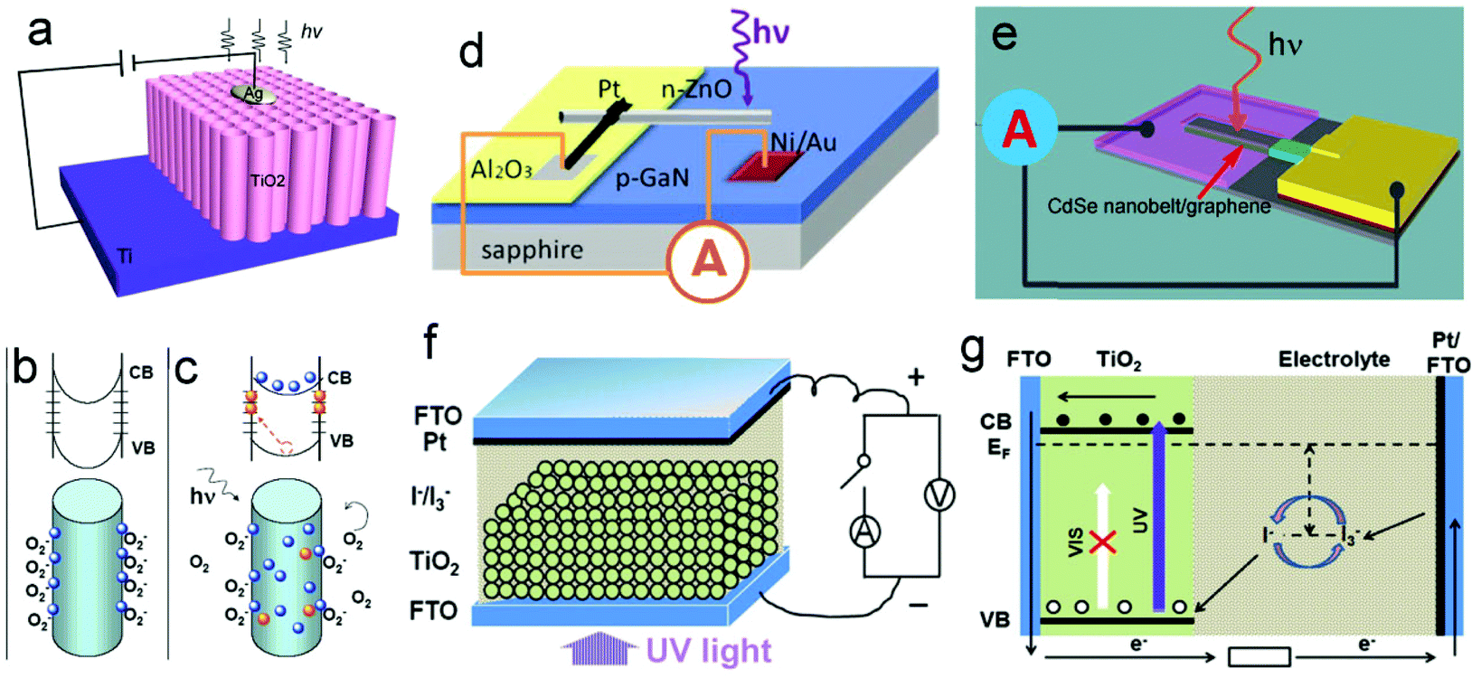 | ||
| Fig. 1 (a) Schematic of a conventional photoconductor based on TiO2 nanotube arrays (TNTAs). (b and c) Trapping and photoconduction mechanism in TiO2 NWs. (d) Schematic of a ZnO–GaN p–n junction. (e) CdSe/graphene Schottky junction UV-PDs. (f) Schematic of self-powered UV-PDs based on PEC cells, and (g) working mechanism of the PEC UV-PD. (a) and (b and c) Reproduced from ref. 6 and 7, respectively. Copyright © 2010 and 2007 American Chemical Society. (d) Reproduced from ref. 20. Copyright © 2011 Wiley-VCH. (e) Reproduced from ref. 21. Copyright © The Royal Society of Chemistry 2012. (f) Reproduced from ref. 22. Copyright © 2012 Elsevier Ltd. | ||
Generally, the performances of a photoconductive PD involve two aspects, namely the absorption of the incident light and the separation/transport of photogenerated electrons.12–14 The magnitude of the conductivity change depends on the quantum yield of carrier generation and the mobility of photogenerated carriers. As schematically shown in Fig. 1b and c, the photo detecting process is normally determined by the absorption and desorption of oxygen molecules in air, both of which are slow processes that lead to a low photoresponse.15–19 Moreover, this type of UV-PD usually needs an external power source, which will limit its potential applications in a harsh environment.
To solve the aforementioned problems, Schottky and p–n junctions are introduced into self-powered UV-PDs, which in nature are optoelectronic conversion devices similar to solar cells. The self-powered UV-PDs based on p–n junctions are constructed using a pair of p- and n-type semiconductors with a wide band gap, forming a p–n junction photodiode (Fig. 1d).23,24 This type of photodiode can convert the incident light into an electrical signal without the necessity of an external power source. Furthermore, the photodiode usually possesses a good spectral selection (visible-blind) and a fast photoresponse (rise time (tr) of several tens of μs, decay time (td) of several hundreds of μs). As illuminated in Fig. 1e, a UV-PD based on the Schottky junction is constructed using a metal/semiconductor interface, in which the semiconductor possesses a wide band gap. When illuminated by UV light (photon energy is larger than the Eg of the used semiconductor), the electron–hole pairs are generated and quickly separated due to the built-in electric field induced by Schottky junctions, showing a photovoltaic (PV) effect. Schottky-junction PDs often show extremely high photosensitivity (ratio of (Iphoto − Idark)/Idark) and fast photoresponse (less than 100 μs).25,26 Although many achievements have been obtained, especially ultra-fast photoresponse and extremely high photosensitivity, the reported self-powered PDs based on p–n or Schottky junctions usually show low spectral responsivity and high cost (a complex fabrication process), limiting their real applications.27
Recently, photoelectrochemical (PEC) self-powered UV-PDs have attracted great attention.22 As shown in Fig. 1f, this type of UV-PD possesses a similar device configuration to other PEC devices, which, in principle, is a PEC PV device. Fig. 1g shows the working mechanism of the PEC UV-PDs using a wide-band-gap semiconductor as the photoanode. When the nanocrystalline TiO2 (nc-TiO2) film is illuminated by UV light, the absorbed photons will promote electrons from the valence band (VB) to CB, eCB, leaving behind a hole, T+:
| T + hν → T+ + eCB. |
The photogenerated holes then migrate to the semiconductor/electrolyte interface and trap an electron donor in the electrolyte (D), leaving the oxidized redox species, D+,
| T+ + D → T + D+, |
| D+ + e → D. |
Therefore, in this type of PEC UV-PD, light harvesting and photogenerated carrier transport are achieved simultaneously.
Compared to the reported self-powered photoconductors based on p–n junctions and/or Schottky junctions, PEC UV-PDs usually exhibit two advantages:28–34 (1) much higher photo responsivity. Most of the reported p–n junctions and/or Schottky junctions are made up of semiconductor nanoscale units, which usually lead to current output signals of nA order and require high-precision galvanometers; while PEC UV-PDs can output a large current of μA order. (2) Simple fabrication processes and low cost: the fabrication of p–n junctions and/or Schottky junctions usually requires not only complex processes, but also high-purity semiconductor raw materials, both of which determine their high cost; while PEC UV-PDs are usually fabricated via a physicochemical route, which shows a low requirement in fabrication and cost. Nevertheless, this proposal of PEC UV-PDs might open a new insight into the development of cheap, easily-fabricated, self-powered UV-PDs with high spectral responsivity, high photo sensitivity and fast photoresponse.
The aim of this review is to sum up recent advances in PEC self-powered UV-PDs, including (1) the basics of performance evaluation of PEC UV-PDs for an easy understanding of different research approaches and diverse performance metrics reported in the literature; (2) the latest developments in electrolyte and photoanode designs for PEC UV-PDs, including various electrolytes, various wide-band-gap semiconductors, and various micro-/nano-scale morphologies/modifications/hybrids; and we further analyze their effects on the properties of photoanodes (such as power conversion efficiency (η), photocurrent density (J), spectral responsivity, and photosensitivity). In this context, we provide examples from recent experimental results to elucidate these concepts in this section. And we will finally give an outlook on future directions in the research on PEC UV-PDs aiming to excite more research interest and stimulate further research progress in this research field.
2 Performance evaluations of PEC UV-PDs
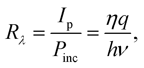
The basic performance metrics of a PEC self-powered UV-PD usually include spectral responsivity, photosensitivity, response time, incident photo-to-current conversion efficiency (IPCE), etc.28,31–36 These parameters indicate how a detector responds and are described as follows:Spectral responsivity (Rλ, A W−1) is the ratio of photocurrent (Ip) to incident light power. It mainly depends on the wavelength of incident UV light. The plot of responsivity as a function of wavelength gives the spectral response of a PD. The Rλ can be evaluated using
Photosensitivity (S), named as the ON/OFF ratio, is the ratio between Ip and dark current (Id), i.e.,
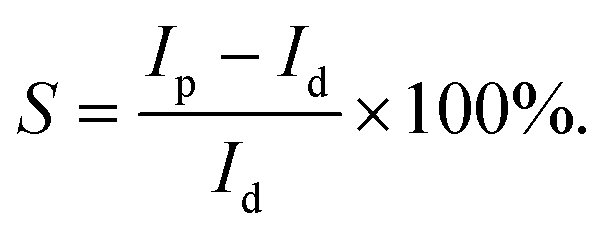
This ratio depends on both Ip and Id, reflecting not only the optoelectronic conversion performances of the devices, but also the transport characteristics of electrons in the devices’ photoanodes.
Response time (t) is used to characterize the speed of response to a sudden change in the input signals, i.e., to measure the time required for a PD's response to a light pulse. The response time is specified as the time taken by the photocurrent to rise or decay to a specific value under the “ON” or “OFF” state of light illumination. The tr is often defined as the time taken by the photocurrent to increase from 0 to 63% (i.e., 1 − 1/e) of the maximum value, and the td is the time taken by the photocurrent to decrease from the maximum value to 37% (i.e., 1/e).
In most cases of PEC UV-PDs, the response speed is limited by the td, rather than the tr, which is quite different from other types of UV-PDs.37 In fact, the tr of a PEC UV-PD is mainly dependent on two fundamental aspects: (1) the time taken by the eCB generated in the solid/liquid interface to diffuse to the TCO electrode via the wide-band-gap semiconductor films; (2) the time taken by the D+ to drift to the counter electrode via the electrolyte. The drift process of D+ through the electrolyte is usually quite rapid due to free ion transport in the electrolyte, while the eCB diffusion process is greatly influenced by the recombination time and is relatively slow. The diffusion time can be improved by ensuring that all electron–hole pairs are separated and transported through the electrode films under the built-in electric field of the semiconductor junctions.
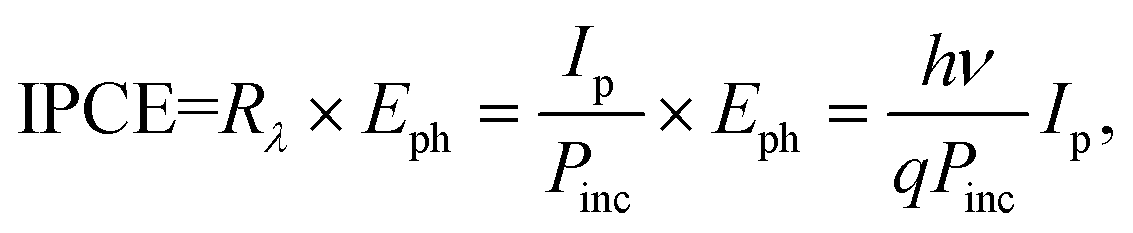
IPCE is defined as the ratio of output Ip (electrons per second) to incident photon fluence (photons per second) on the device. It mainly depends on the light harvesting efficiency (LHE (λ)), electron injection efficiency (ϕinj), and electron collection efficiency (ηc). Then IPCE can be roughly expressed by38
| IPCE(λ) = LHE(λ) × ϕinj × ηc. |
Thus, what we can do to increase the IPCE value is to improve LHE(λ), ϕinj and ηc, which generally guide the potential research directions in the PEC field. On the other hand, using Rλ, IPCE can also be estimated using
Some important issues should be noted here for graduate students or researchers who are new in the research on PEC UV-PDs. First, the methodologies to reliably choose and prepare a material for use as an PEC UV-PD electrode are not well standardized due to the reported different techniques and parameters (e.g. different device structures (three-electrode or two-electrode), different calculations of response time (0 to 1 − 1/e, 0 to 90%, or 0 to a stable value), different electrode kinds/materials/morphologies, different electrolytes/ions, and different UV light wavelengths), thus yielding widely varying results. Second, the requirements in electrode materials are not the same as those in dye sensitized solar cells (DSSCs) or photocatalytic cells; e.g., the IPCE value is not the most important parameter for PEC UV-PDs. Third, for a high-performance UV-PD, it should be “visible-blind” for high UV selection, and “linear output” for quantitative UV measurement. This is to say, these two aspects are also important performance metrics for UV-PDs.
Overall, the various performance metrics discussed above indicate that the UV detection performances of the PEC devices are mainly determined by the photoanodes. Current research efforts are focused on improving the optoelectronic performance of the frequently-used photoanode materials (such as ZnO, TiO2 and SnO2), including spectral responsivity, photosensitivity, response time, visible-blind and linear-output characteristics. In addition, the used electrolytes and multi-functional PEC UV-PDs are also briefly reviewed, as well as the preparation of the micro-/nano-structure of photoanodes. The recent results are summarized in Table 1.
| Nanostructures | Conditions | Electrolyte type | Electrode system | J p (μA cm−2) | S ((IP − Id)/Id) | t r (s) | t d (s) | Estimate method of t | R λ (mA W−1) | Visible blind | Linear output | Ref. |
|---|---|---|---|---|---|---|---|---|---|---|---|---|
| Hydrothermal ZnO NRs | 250–600 nm, 100 mW cm−2, 0 V | 0.1 M Na2SO4 | 3-Electrode | 1.5 | 7 | 4.9 | 134.3 | Biexponential function fitting | — | No | — | 39 |
| ZnO(N) NR films | 390 nm, 3 mW cm−2 | Spiro-MeOTAD | 2-Electrode | 50 | 300 | 4 × 10⁻³ | 1 × 10⁻² | 10% to 90% | 17 at 390 nm | Yes | — | 40 |
| TiO2 NRAs | 365 nm, 0.7 mW cm−2 | Poly(9,9-dihexylfluorene) | 2-Electrode | 1.78 × 10⁻² | 1000 | <0.2 | <0.2 | Estimated by the test limit | 33 at 395 nm | Yes | — | 41 |
| ZnO nanoneedles | 365 nm, 1.25 mW cm−2 | DI water | 2-Electrode | 4.1 | — | 0.1 | 0.1 | 10% to 90% | 22 at 385 nm | Yes | No | 30 |
| ZnO@TiO2 nanostrawberries | 365 nm, 20 mW cm−2 | I−/I3− | 2-Electrode | 379 | 37![[thin space (1/6-em)]](https://www.rsc.org/images/entities/char_2009.gif) 899 899 |
0.022 | 0.009 | 0–1, 1 − e−1 | 17.85 at 365 nm | Yes | Yes | 29 |
| ZnS/ZnO NRAs | Xe lamp, 100 mW cm−2, 0 V | 0.5 M Na2SO4 | 3-Electrode | 50 | — | — | — | — | — | Yes | — | 42 |
| TiO2 films by ALD | 365 nm, 2.44 mW cm−2 | Water | 2-Electrode | 100 | 106 | <0.5 | <0.5 | 0 to 1 | 69 at 350 nm | Yes | Yes | 43 |
| nc-TiO2 films | 365 nm, 33 mW cm−2 | I−/I3− | 2-Electrode | 550 | 2698 | 0.08 | 0.03 | 0–1, 1 − e−1 | 16.7 at 365 nm | Yes | Yes | 22 |
| TiO2 NRAs | 365 nm, 3 mW cm−2, 0 V | 0.5 M Na2SO4 | 3-Electrode | 15 | 6 | <0.1 | <0.1 | — | 5 at 365 nm | — | No | 44 |
| TiO2 NRAs | 365 nm, 10 mW cm−2 | DI water | 2-Electrode | 40 | — | 0.15 | 0.05 | 0–90%, 1 − e−1 | 25 at 350 nm | Yes | — | 36 |
| TiO2 NRAs | 365 nm, 2.5 mW cm−2 | Liquid crystal- I−/I3− gel | 2-Electrode | 175 | — | <0.03 | <0.03 | 0–90%, 1 − e−1 | 90 at 383 nm | Yes | Yes | 33 |
| TiO2 nano-branched arrays | 365 nm, 2 mW cm−2 | I−/I3− | 2-Electrode | 373 | — | 0.15 | 0.05 | 0–90%, 1 − e−1 | 220 at 352 nm | Yes | — | 34 |
| Dendriform TiO2 NWs | 365 nm, 25 mW cm−2 | I−/I3− | 2-Electrode | 570 | 1902 | 0.0053 | 0.0059 | 0–1 − e−1, 1 − e−1 | 22.8 at 365 nm | Yes | Yes | 45 |
| TNRCs | 254/365 nm, 1.55 mW cm−2, 0 V | I−/I3− | 2-Electrode | 17 | — | 1.7 | 2.1 | 0 to 1 | 19 at 345 nm | Yes | Yes | 35 |
| TNRs | 235 | — | 0.3 | 0.1 | 89 at 355 nm | Yes | Yes | |||||
| Multilayer TNRC/TNRs | 278 | — | 0.3 | 0.2 | 152 at 360 nm | Yes | Yes | |||||
| TNTAs | 250–385 nm, 0 V | 0.1 M NaOH | 3-Electrode | 210 | — | <0.2 | <0.2 | 0–1 | 11.2 at 350 nm | Yes | — | 46 |
| SrTiO3–TiO2 heterojunction | 650 | — | <0.2 | <0.2 | 18.6 at 350 nm | Yes | — | |||||
| B-SnO2 NFs | 365 nm, 40 mW cm−2 | I−/I3− | 2-Electrode | 900 | 4549 | 0.03 | 0.01 | 0–1, 1 − e−1 | 22.5 at 365 nm | Yes | Yes | 28 |
| SnO2@TiO2 microtubes | 365 nm, 1.55 mW cm−2 | I−/I3− | 2-Electrode | 100 | — | <0.1 | <0.2 | 0 to 1 | ∼52 at 340 nm | Yes | — | 32 |
| SnO2 microtubes | 78 | — | <0.1 | <0.2 | ∼38 at 340 nm | Yes | — | |||||
| SnO2@TiO2 hollow nanospheres | 365 nm, 35 mW cm−2 | I−/I3− | 2-Electrode | 1277 | 4020 | 0.03 | 0.01 | 0–90%, 1 − e−1 | 36.48 at 365 nm | Yes | Yes | 31 |
| B-TiO2 nanoneedles–SnO2 nanosheets | 365 nm, 40 mW cm−2 | I−/I3− | 2-Electrode | 709.5 | 4404 | 0.02 | 0.004 | 0–1, 1 − e−1 | 17.7 at 365 nm | Yes | Yes | 47 |
3 Recent developments in PEC UV-PDs
3.1 Prototype for PEC self-powered UV-PDs
PEC UV-PDs possess a similar device configuration to other PEC devices, evolved from a photoanode/electrolyte/counter electrode sandwich structure. Thus their working mechanisms are to some extent the same as that of other PEC devices. Generally, the improvement in detecting the performances of PEC UV-PDs hinges on the development of the combination of electrolytes (redox couples), counter electrodes, and photoanodes.48 In 2011, Lee et al. first reported a type of UV-PD based on a TiO2/water solid–liquid heterojunction,43 containing two electrodes: a 50 nm TiO2/Fluorine-doped Tin Oxide (FTO) electrode and 50 nm Pt/indium tin oxide (ITO). Both electrodes were assembled together using a sealant and some water used as an electrolyte was poured into the space between them. Under UV illumination (365 nm, 0.244 μW cm−2 to 0.113 mW cm−2), the Ip of the devices linearly increases with increasing incident light power, exhibiting an excellent reproducible photoresponse with a fast response speed (both decay and rise times are less than 0.5 s). Here, it is noted that this linear variation of Ip will make this type of UV-PD easily usable for the quantitative measurement of UV light. Moreover, the S can reach an order of magnitude of 6 under 479 μW UV illumination, and the devices show a visible-blind characteristic, exhibiting their maximum responsivity of ∼69.2 mA W−1 at ∼350 nm. Thus, it can be seen that this type of UV-PD possesses an exceptional competence for UV light detection and presents a promising direction for future development of commercially low-cost UV-PDs.Alternatively, the three-electrode configuration is also adopted to test the electrochemical performances of electrode materials. For instance, Majumder et al.39 tested the PV response of hydrothermal ZnO nanorod arrays (ZnO NRAs) grown on a FTO substrate using a three-electrode system, in which Ag/AgCl served as the reference electrode, a Pt wire as the counter electrode, and 0.1 M Na2SO4 aqueous solution as the electrolyte. The ZnO NRAs show a stable and repeatable PV response, showing a quick increase in PV but a slow recovery. The ZnO NRAs show the maximum PV at 350 nm and good visible-blind characteristics. In a strict sense, this three-electrode configuration is not a real device. However, it is technically more challenging to precisely analyze and discuss limited results from the reported two-electrode PEC cells. So, to give a far and wide discussion on PEC UV-PDs, the results from the three-electrode system have also been put into the whole frame for comparison.
3.2 PEC UV-PDs based on various electrolytes
The electrolyte is one of the most crucial components that provide pure ionic conductivity between the photoanode and counter electrode in PEC UV-PDs.49 Redox electrolytes in UV-PDs can not only function as the medium for the inner carrier transport between electrodes, but also continuously reactivate the semiconductor and itself during the operation. Thus, several aspects are essential for the electrolytes used in PEC UV-PDs: (1) the electrolytes must be able to transport the carriers between the photoanode and counter electrode. Once the electrons are promoted from the VB to CB, the remaining holes will be rapidly oxidized by electron donors in the electrolyte. (2) The electrolytes must guarantee a fast drift of carriers (higher conductivity) and show large interfacial contact with the mesoporous semiconductor photoanode and the counter electrode. (3) The electrolyte should be chemically stable and inert to photoanode materials, which guarantees the efficiency and long-term stability of the PEC devices. According to the physical state, compositions, and formation mechanisms, the electrolytes used in PEC UV-PDs can be broadly classified into: aqueous electrolytes, organic liquid electrolytes, or quasi-solid gel electrolytes. Xie and Shen's groups reported PEC self-powered UV-PDs assembled using the traditional liquid I−/I3− redox couple electrolyte.22,28,29,31,32,35,45,47 And impressive performances were observed in these UV-PDs. However, the liquid I−/I3− redox couple electrolyte is not ideal for long-term operation, because it is highly corrosive, volatile, and photo-reactive, which often makes it interact with common metallic components and sealing materials.Aqueous electrolytes are more suitable for PEC self-powered UV PDs due to the fact that water is one of the safest, most stable, and most environment-friendly electrolytes. And a type of UV-PD based on TiO2/water solid–liquid heterojunction has been proposed recently.30,36,43 Interestingly, this TiO2/water-based UV-PD can exhibit high photosensitivity, excellent spectral selectivity, linear variations in Ip, and fast response.43 Moreover, Chen's group reported that TiO2 NR/water-based self-powered UV-PDs showed a spectral responsivity of 25 mA W−1 and a fast photoresponse.36 Furthermore, many aqueous electrolytes have been used during PEC tests, such as Na2SO439,42,44,50–57 and KOH.58–60 Cao et al. reported the Ip response of TiO2 nanorod arrays (NRAs) under UV illumination using a 0.5 M Na2SO4 aqueous electrolyte,44 in which TiO2 nanostructures can harvest more incident light photons compared to a flat thin-film active layer because of the markedly enlarged TiO2/electrolyte contact area. The photocurrent density (Jp) can reach 12.87 μA cm−2 under UV illumination (365 nm, 3 mW cm−2). Though aqueous electrolytes are safe, stable, and environment-friendly, the performances of these UV-PDs are poorer compared to those with the I−/I3− electrolyte. So, further research is required for the development of the aqueous electrolyte.
Using aqueous electrolytes as the medium for the carrier transport, great developments have been achieved in various PEC devices. However, liquid electrolytes often cause some practical problems, such as leakage, volatilization of solvent, corrosion of counter electrode, and ineffective sealing of the cells for long-term applications. Recently, a type of quasi-solid-state electrolyte has been used in PEC cells. Han et al. demonstrate a high spectrum selectivity from TiO2-NRA-based UV-PDs by using poly(9,9-dihexylfluorene) as the electrolyte.41 The maximum response of 33.2 mA W−1 at 395 nm is obtained under zero bias. However, the Jp is only about 1.78 × 10⁻⁵ μA cm−2 under 0.7 mW cm−2, 365 nm UV illumination. More recently, Chen's group reported nanostructured quasi-solid-state UV-PDs fabricated using a liquid crystal (LC)-embedded I−/I3− electrolyte with a light-trapping scheme.33 The maximum responsivity is about 90 mA W−1 at 383 nm; the maximum IPCE is about 29%. Under 2.5 mW cm−2 UV illumination (365 nm, 0 V), the Jp reaches 175 μA cm−2 with tr less than 0.03 s. Moreover, Game et al. report a facile solution-processed fabrication of a self-powered organic–inorganic hybrid PD using n-type oriented ZnO NRs and a p-type Spiro-MeOTAD semiconductor.40 The assembled UV-PDs show a high S (102), a high UV/visible ratio (300) and a fast photoresponse (tr of 200 μs and td of 950 μs). Under UV illumination (390 nm, 3 mW cm−2), a Jp of 50 μA cm−2 can be obtained. Although the efficiencies of these UV-PDs with quasi-solid-state electrolytes are often lower than those of the UV-PDs with liquid electrolytes, the quasi-solid electrolytes may become viable alternatives to the liquid electrolytes owing to the greatly improved stability and sealing ability, which will be beneficial to their practical applications.
3.3 PEC self-powered UV-PDs based on various photoanodes
So far, most work to enhance the performances of PEC UV-PDs has focused on developing photoanodes with high photoresponse, including spectral responsivity, photosensitivity, and response time. The key findings can be seen in Table 1. Researchers have used different materials, micro-/nano-structures, electrolytes, counter electrodes, and even diverse device structures to report the UV detecting performances of the assembled PDs, which makes it difficult to directly compare some results in the literature. In general, short-circuit photocurrent (Isc) or density (Jsc) of electrode materials is obtained using either the assembled two-electrode cell or the three-electrode system. Moreover, many studies have reported the “visible-blind” and “linear output” characteristics, even though the estimate methods of photosensitivity, ON/OFF ratio, and rise and decay time are not always consistent. Thus, we have listed the different methods used in Table 1 for easy comparison. And it can be seen that various nanostructures were exploited for constructing photoelectrodes in PEC cells, including NPs, NRs, NWs, NTs, NRAs, nanosheets (NSs), and nano-forests.61 It is suggested that the electron transport rates of these nanostructures mentioned above are in the sequence of NP films < NR films < nano-forest films < NRA films, while the sequence for specific surface area (SSA) turns out to be NP films > NR/NW films > nano-forest films > NTA films > NRA/NWA films. Thus, there is a need for a strategy to balance the choice in constructing PEC electrodes.On the other hand, the band-gap energy of the photoanode for UV-detection should be larger than 3.1 eV, corresponding to the wavelength of 400 nm. The recently reported wide-band gap oxide nanostructures (including binary metal oxides like ZnO (ZnS),42 TiO2,11 SnO2,62 NiO,63 Nb2O5,64 Ga2O3,65 ZrO2,66 and ternary metal oxides like SrTiO364) can be potentially applied as photoanode materials for PEC UV-PDs (Fig. 2). So far, ZnO, TiO2 and SnO2 are the most frequently studied materials for PEC cells, and in this context, we present them in three sub-sections, i.e. ZnO, TiO2, and SnO2 nanostructured photoanodes.
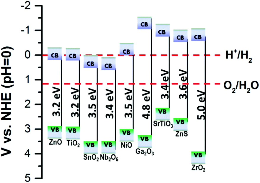 | ||
| Fig. 2 Schematic diagrams of the energy levels of the CB and VB of various wide-band-gap semiconductors. | ||
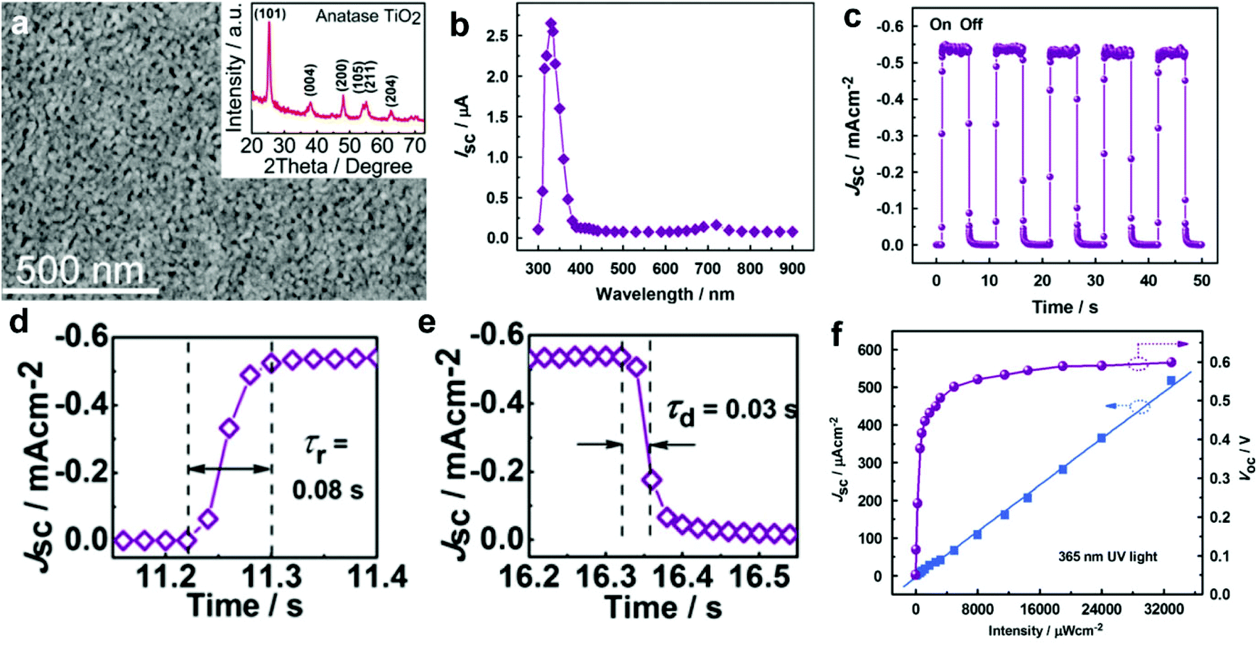 | ||
| Fig. 3 (a) SEM image of the spin-coated TiO2 films; the inset is the corresponding XRD spectrum; (b) spectral responsivity of the self-powered UV-PDs, indicating a visible-blind characteristic; (c) time responses of Jsc under UV illumination (365 nm, 33 mW cm−2) measured for light-on/off states; (d and e) enlarged rise and recovery edges of the current response at a light intensity of 33 mW cm−2, respectively; (f) Jsc and Voc as a function of the incident UV (365 nm) intensity. Reproduced from ref. 22. Copyright © 2010 Elsevier Ltd. | ||
Another suitable nanostructure of TiO2 for UV-PDs is vertical NRAs due to their relatively high transport rates of electrons and enhanced transfer of electrolyte ions because of more interfaces between the NRs and the solution compared to a flat thin-film active layer. It is demonstrated that the basic parameters of NRAs (such as diameter, length and density) greatly affect the performances of PEC cells. Cao et al.44 found that under UV illumination (365 nm, 3 mW cm−2, 0.5 M Na2SO4, three-electrode system), 3 μm long TiO2 NRAs show a Jp of about 15 μA cm−2, while 6 μm long TiO2 NRAs only 6 μA cm−2, suggesting that a suitable length of NRAs is required for a high Jp. In view of this point, Chen's group applied vertical rutile TiO2 NRAs (∼1 μm in height, 100–150 nm in diameter, 20 NRs per μm2 in density) to PEC UV-PDs (Fig. 4a and b).36 Under UV illumination (365 nm, 1.25 mW cm−2, DI water), the Jp is 4.67 μA cm−2 with the Rλ of 4 mA W−1. This low responsivity should be mainly attributed to the high resistance of the used water electrolyte. Meanwhile, this device shows a fast photoresponse, i.e., a tr of 0.15 s and a td of 0.05 s, indicating a rapid photoresponse characteristic. Moreover, the maximum responsivity of the photoanodes reaches about 25 mA W−1 at 350 nm.
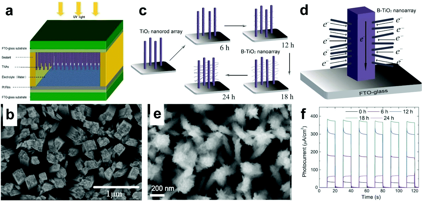 | ||
| Fig. 4 (a) Schematic device structure of the PEC UV-PDs using water as the electrolyte, and (b) top-view SEM image of TiO2 NRAs. (c) Schematic formation process of B-TiO2 NRAs grown on FTO glass, (d) scheme of the possible electron transport mechanism in a B-TiO2 NRA photoanode, (e) top-view SEM image of B-TiO2-18 h NRAs, and (f) time responses of Jp values for different PDs under UV light pulsed illumination (365 nm, 2 mW cm−2). (a and b) Reproduced from ref. 36. Copyright © 2013 Springer. (c–f) Reproduced from ref. 34. Copyright © 2014 IOP Publishing. | ||
Compared to NRAs, TiO2 NTAs (TNTAs) are also attractive in the field of PEC applications, such as DSSCs, photocatalysts, and UV-PDs, due to their enlarged TiO2/electrolyte interface and well-defined carrier transport path, and most importantly, ease of fabrication and low cost.6,69 Li et al.59 reported that under UV illumination (365 ± 15 nm, 70 mW cm−2, 0 V bias), the 3 μm long TNTAs exhibit a Jp of ∼100 μA cm−2 with the Rλ of 1.4 mA W−1. And the Jp can also quickly drop to zero when switching off the light source, indicating fast charge transport in NTAs. However, compared to the nc-TiO2, both TiO2 NRA and NTA films show a much lower Rλ, which may be due to their lower SSA and thus lower light harvesting efficiency.
It is reported that branched TiO2 (B-TiO2) nanostructures (i.e., nano-forest) usually possess better charge transport and light absorption properties than NP films, and larger SSAs than NRAs/NTAs.70–72 Chen's group prepared B-TiO2 NRAs by a facile two-step chemical synthesis process and assembled them into photoanodes (Fig. 4c and d).34 Under UV illumination (365 nm, 2 mW cm−2), the assembled PEC UV-PDs (18 h, Fig. 4e and f) also exhibit a high Jp of 373 μA cm−2 with the Rλ of 186.5 mA W−1, which is greatly enhanced compared to those of the above single-phase TiO2 NRA/NTA and nc-TiO2 films. Moreover, the UV-PDs also show a fast photoresponse (tr of 0.15 s and td of 0.05 s). These improved performances are attributed to a markedly enlarged TiO2/electrolyte contact area and a high electron conductivity in the TiO2 NR trunk. However, it can be seen that the enhanced light scattering by B-TiO2 NRAs leads to lower transmission in the visible light region, which is harmful to spectral selectivity of a UV-PD.
ZnO NRAs/NWAs have also been frequently used in PEC cells, such as water splitting and PV systems, due to their good conduction of electrons and holes, nontoxicity, environment friendliness, and controllable low-temperature synthesis.76,77 Compared to NP films, NRAs usually possess higher light absorbance efficiency and lower electron recombination. Recently, Chen's group reported a type of PEC UV-PD using hydrothermal-grown ZnO nanoneedles as the active photoanode and DI water as the electrolyte (Fig. 5a).30 The resultant ZnO nanoneedles possess an average length of 2–3 μm and a diameter of 80–100 nm at the base (Fig. 5b). The maximum Rλ of ZnO nanoneedle arrays is ∼22 mA W−1 at ∼385 nm, showing good spectral selectivity in the UVA range. Under UV illumination (365 nm, 1.25 mW cm−2), the JP is 4.08 μA cm−2 with the Rλ of 3.26 mA W−1. Both tr and td of the device are ∼0.1 s for Jsc, which will make ZnO nanoneedle arrays show potential application in UV-PDs. However, the photoresponse region is obviously broadened to over 450 nm because of the light scattering between nanoneedles. This is unfavorable to UV detection. It is found that there exists a gradual saturation in Jp under higher UV illumination, which might be due to the poor carrier transportability of water.
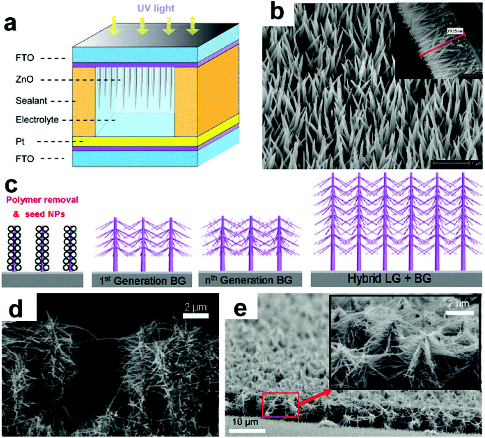 | ||
| Fig. 5 (a) Schematic device structure of UV-PDs based on ZnO nanoneedle arrays and (b) SEM image of ZnO nanoneedle arrays; the inset shows their cross-sectional view. (c) Schematic growth route for ZnO NWAs with different branches, (d and e) SEM images of ZnO NWAs after one time branched growth and ZnO NW nano-forest, respectively. (a and b) Reproduced from ref. 30. Copyright © 2013 Springer. (c–e) Reproduced from ref. 78. Copyright © 2011 American Chemical Society. | ||
Hierarchical branched nanostructures are other promising structures that provide a high light absorption for the optoelectronic devices.79 Ko et al.78 studied the effect of branched growth on the efficiency of hierarchical ZnO NWA photoanodes (Fig. 4c–e), and found that after one-time branched growth, the Jsc of 7 and 13 μm ZnO NWAs are significantly enhanced 389% and 256% compared to the pristine ones, respectively; while with one more branched growth, the Jsc of 13 μm ZnO NWAs can be further slightly enhanced ∼14%. Thus, this Jsc increase can be explained by considering a combination of several effects:80 (i) enhanced light absorption from the enlarged SSA results in a large Jsc increase. (ii) The dense network of crystalline ZnO NWs can increase the electron diffusion length and electron collection because the NWs provide direct conduction paths for electrons’ transport from the injection points to the collection electrode. (iii) Randomly branched NWs promote enhanced light-harvesting without sacrificing efficient electron transport. Furthermore, branched NWs also increase light-harvesting efficiency by scattering enhancement and trapping, which might be unfavorable to spectral selectivity of the assembled UV-PDs.
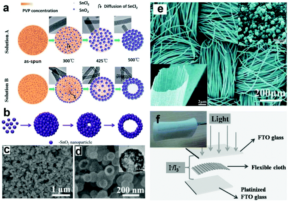 | ||
| Fig. 6 (a) Schematic formation mechanism of SnO2 NFs and NTs. (b) Schematic illustration of the formation of SnO2 HNS, (c and d) SEM images of the prepared SnO2 HNSs; the inset in (d) is the TEM image. (e) Typical SEM images of SnO2 cloth woven by microtubes; the insets show amplified SEM images of a single SnO2 microtube assembled by numerous NPs. (f) Structure scheme of the PEC UV-PDs; the inset shows an optical image of SnO2 cloth. (a) and (e) Reproduced from ref. 81 and 82, respectively. Copyright © 2012 and 2013 The Royal Society of Chemistry. (b–d) Reproduced from ref. 31. Copyright © 2014 Elsevier Ltd. (f) Reproduced from ref. 32. Copyright © 2014 Wiley-VCH. | ||
More recently, Shen's group has prepared a type of SnO2 microtubes using carbon cloth as sacrificial templates,32,82 which can be directly used as a binder-free photoanode (Fig. 6f). These microtubes consist of rutile SnO2 NPs with the size of several tens of nanometers (Fig. 6e). The assembled PEC UV-PDs using the I−/I3− electrolyte show a high Jp response of 78 μA cm−2 with the Rλ of 50.3 mA W−1 under UV illumination (365 nm, 1.55 mW cm−2). Compared to TiO2-based photoanodes, the poor performances observed from SnO2 ones are mainly attributed to the fast interfacial electron recombination and lower trapping density.84 Thus in a later section, we will give a review on recent studies of the PEC performances of SnO2-based hybrid photoanodes, including SnO2 NF/NP, and SnO–TiO2 hybrids.
3.4 Modification of photoanodes for high-performance UV-PDs
Similar to an optoelectronic cell, the strategies for enhancing the performance of PEC PDs usually include three aspects, i.e., enhancing light harvesting in photoanodes (for high Rλ and S), enhancing charge separation or reducing charge recombination (for a repeatable and fast Jsc response), and enhancing charge transport (for short tr and td). In this section, we will give a systematic introduction to these three strategies and detailed discussions on the design of photoanodes for high-performance PEC UV-PDs.3.4.1.1 Porous films. On entering a porous NP layer, the incident light can generally be divided into two parts: (i) one part is adsorbed by NPs, and (ii) the other part is penetrating the NP film after multiple refractions, which can increase the light harvesting. Then, based on this point, Mridha et al.85 prepared a type of sponge-like porous ZnO with the assistance of activated carbon (AC). This AC-assisted ZnO (AC-ZnO) shows a SSA of 3.17 m2 g−1, which is increased by 33% compared to that of the bare ZnO (B-ZnO). The UV absorption of AC-ZnO in the range of 300–400 nm is enhanced 10% compared to that of B-ZnO. Moreover, the S of AC-ZnO is 162, which is four times greater than that of B-ZnO. And both tr and td of AC-ZnO are 5–6 times shorter than those of B-ZnO, indicating a fast photoresponse. Moreover, Hu et al.86 fabricated a type of mesoporous TiO2 photoanode via a gel hydrothermal method using PVP as a pore-forming agent. It is found that the absorbance of TiO2-1.5 wt% films is enhanced 23% in the UV region compared to that of dense TiO2 films, implying that the multiple refractions can greatly enhance the light absorption efficiency in TiO2 photoanodes. And the counterpart PEC cells yield an η of 9.86%, which is enhanced 53.8% compared to that of the dense TiO2 ones. This enhancement in η suggests that the porosity and pore size of TiO2 photoanodes not only enhance the light harvesting efficiency, but also affect the SSA of photoanodes for greatly enhanced electrolyte ion adsorption and interfacial charge transfer. Furthermore, Lei et al.53 studied the effect of pore size on the optoelectronic performances of the porous films prepared via the sol–gel technique using polystyrene (PS) sphere templates. Under UV illumination (369 nm, 32 mW cm−2), the Jp of the arrayed 190 nm pore films is 10 μA cm−2, which is ∼5 and 10 times as high as those of the 850 nm pore and nonporous films. The sample with a smaller pore size has larger SSA and is more effective in the improvement of the photocurrent.
3.4.1.2 Lengthwise NRAs. Generally, the insufficient SSA of NWAs constrains the Jsc to relatively low levels due to their low light absorbance. Ko et al.78 performed a parametric study of the effect of NWA length on the efficiency of the photoanodes (Fig. 7a), and found that as the length of ZnO NWAs increases from 7 to 18 μm, the Jsc and η values are enhanced by 90% and 89%, respectively. This increase in Jsc and η is mainly due to the effective SSA increase. Moreover, Xie's group also studied the effect of NWA length on Jsc and η (Fig. 7b),87 and found that on increasing the length of the NWAs from 6 to 23 μm, the Jsc and η values are enhanced by 285% and 283% respectively. It is noted here that the η increases by 85% when the NWA length increases from 6 to 19.4 μm, while it increases by 105% when the NWA length increases slightly from 19.4 to 23 μm. This increasing rate of enhancement is found to be due to the porous structure of ZnO NWs formed by etching during the long-time hydrothermal growth process. To avoid this situation, Xu et al.88 demonstrate a convenient approach for synthesizing multilayer assemblies of ZnO NWAs (Fig. 7c–e), and found that the assembled four-layer ZnO NWAs possess an internal SSA more than 5 times larger than that of single-layer NRAs, and yield a high η of 7%, which is ∼2.3 times higher than that of single-layer NRAs.
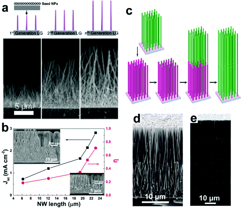 | ||
| Fig. 7 (a) Schematic growth route for ZnO NWAs with different NW lengths; their SEM images are shown in the bottom. (b) Jsc and η of ZnO NWAs as a function of NW length; the inset SEM images show the morphology changes of ZnO NWs. (c) Schematic process for synthesizing the multiple-layer assembly of ZnO NRAs and (d and e) SEM images of two- and four-layer assembly of ZnO NRAs, respectively. (a) and (c–e) Reproduced from ref. 78 and 88, respectively. Copyright © 2011 American Chemical Society. (b) Reproduced from ref. 87. Copyright © 2014 Elsevier Ltd. | ||
3.4.1.3 Densitywise NWAs. Apart from length, the density of NW in an array can also affect the optoelectronic performance of the electrodes, especially light absorption in the visible region due to light scattering, which is unfavorable to UV detection. Hu et al.90 designed various densities of ZnO NRAs using square patterns, and found that the patterned ZnO NRAs show a slight increase in UV absorption, and a large increase in visible absorption. Thus, a suitable density of NWA is required for low absorption in the visible region. In view of this point, Xie's group has prepared a type of dense dendriform TiO2 (D-TiO2) NWAs to serve as the photoanode of PEC self-powered UV-PDs.45 The aspect ratio of the NWs is up to 150 and the surface density is about 90–110 NW μm−2. The grown branches possess a cone shape with an average length of 80 nm and a base diameter of about 15 nm, densely filling the interspace between TiO2 NWs. The UV light absorption of D-TiO2 NWA films is enhanced ∼45% compared to that of TiO2 NWA, and with a very low light absorption in the visible region. And under UV light illumination (330 nm), the Jsc of D-TiO2 NWA films is respectively enhanced 176% and 46% compared to those of TiO2 NWA and nc-TiO2 films. Especially, the responsivity in the visible region drops 1/396 for Jsc as compared with the peak value, indicating a visible-blind property. Under UV illumination (365 nm, 25 mW cm−2), the Jsc value exceeds 570 μA cm−2 with the Rλ of 22.8 mA W−1 and the S of 1902. The tr and td of the D-TiO2 NWA based PEC cell are ∼5.3 and 5.9 ms for Jsc, which is much faster than the photoconductivity-based UV detectors made by 1D TiO2 nanostructures.2,74 In addition, the Jsc increases linearly on increasing the UV light intensity in a wide variation range from 0.05 to 27 mW cm−2, showing a potential application for measuring UV intensity.
3.4.1.4 3D hierarchical architectures. Recently, Shen's group has reported a type of flexible and transferable TiO2 NR cloth (TNRC) synthesized using carbon cloths as sacrificial templates, as illustrated in Fig. 8a.89 The as-synthesized TNRCs are assembled by numerous aligned TiO2 NRs with diameters of about 100 nm (Fig. 8b), showing good transferability and flexibility (Fig. 8c). Illuminated by UV light (365 nm, 1.25 mW cm−2, −1 V), the assembled sandwich device without an electrolyte show an R of only ∼10 mA W−1, a tr of ∼1.4 s, and a td of ∼6.1 s. These low optoelectronic performances are due to the relatively lower film thickness and NR density compared to the traditional NP films, and a large proportion of the photons will become transmission loss for TNRCs. Then, Shen's group further tried to combine multilayers of TNRCs with vertical TiO2 NRs (TNRs), and obtained a type of 3D hierarchical TNRC structures.35 It is found that the use of the hierarchical 3D TNRC structures can greatly reduce the “transmission loss” problem in TNRC films (Fig. 8d and e). And the IPCE of the TNRCs combined with TNRs increases from ∼32.5% to ∼45% at ∼360 nm. Although the spectral response range is slightly widened, the photoresponse is still narrow enough to meet the “visible blind” property (Fig. 8f). Under UV illumination (365 nm, 1.55 mW cm−2, inset of Fig. 8f), the PEC UV-PDs based on TNRC@TNRs using the I−/I3− electrolyte show a much higher photoresponse of 278 μA cm−2 with an R of 179 mA W−1, which is enhanced 18% compared to that of TNRs. Moreover, the tr and td of TNRC@TNRs are 0.3 and 0.2 s, respectively. This indicates that introducing TNRC into UV-PDs increases the photoresponse by reducing light transmission, while retaining the carrier transport efficiency. Furthermore, all devices can not only respond to very weak optical signals, but also show highly-linear properties, which can make them ideal candidates for UV radiation-level measurement. However, the 30% increase in light absorption only leads to a 12% increase in IPCE, which is mainly due to the poor attachment existing between the TNRCs and the TNRs. Nevertheless, this type of freestanding multilayer nanostructured photoanode opens a new route for fabricating high quality UV-PDs with a fast and high response.
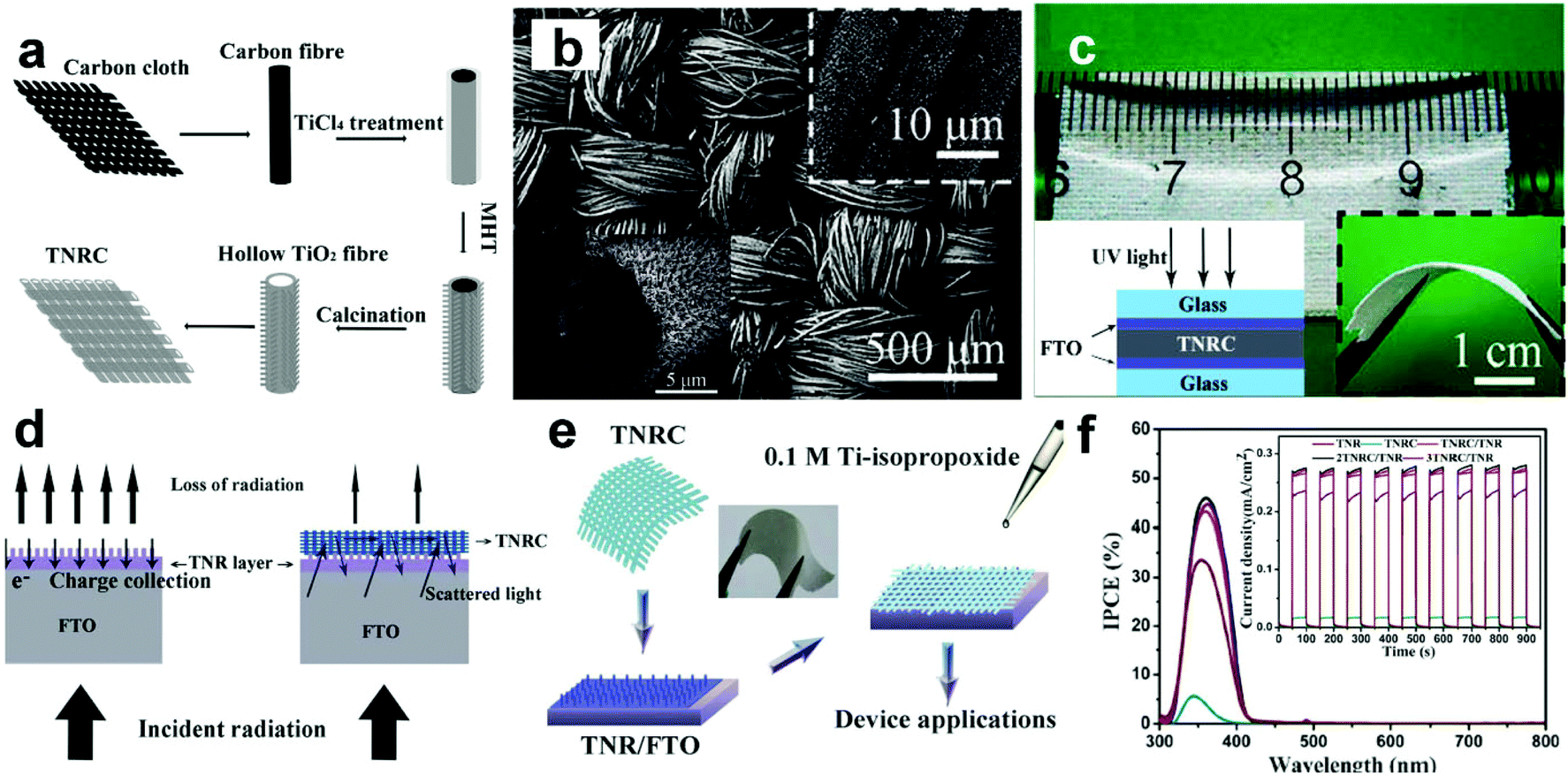 | ||
| Fig. 8 (a) Scheme for fabricating the TNRCs, (b) top-view SEM image of the TNRCs; the insets show enlarged top and cross-sectional view SEM images, respectively, and (c) optical images of TNRCs under a ruler, and the inset (right) shows their optical image under bending. (d) Design and principles for the TNRC/TNR structure to achieve better performance, (e) scheme for fabricating the TNRC/TNR structure, and (f) IPCE testing for the PEC PD; the inset shows photoresponse of different PEC detectors under UV light rectangular pulses (365 nm, 1.55 mW cm−2). (a–c) Reproduced from ref. 89. Copyright © 2011 American Chemical Society. (d–f) Reproduced from ref. 35. Copyright © 2012 The Royal Society of Chemistry. | ||
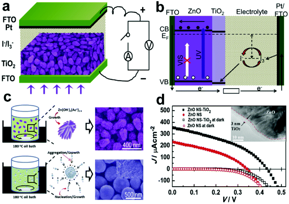
3.4.2.1 ZnO-based core–shell structures. The high Id in ZnO nanostructured photoanodes caused by photo-corrosion in aqueous solution will greatly limit the photosensitivity of the devices. Thus, coating a layer of TiO2 on ZnO nanostructures can effectively protect the ZnO NWs from degradation and corrosion in basic media under light illumination.92 Moreover, it is also demonstrated that the Id was largely blocked and the Jsc was increased because of the CB offset of 0.1 eV and the VB offset of 0.2 eV between the ZnO core and the TiO2 shell (Fig. 9b).93–95 In 2013, Xie's group reported a type of PEC UV-PD based on ZnO@TiO2 core–shell nanostrawberries (ZnO NS-TiO2) using the traditional I−/ I3− electrolyte (Fig. 9a).29 The resultant TiO2 shell is 3 nm in thickness (inset of Fig. 9d), and the ZnO-NS core is ∼250 nm in length, ∼155 nm at the big side, ∼91 nm at the small side, consisting of ∼22 nm rod-like NPs (SEM image in Fig. 9c). Under UV illumination (365 nm, 20 mW cm−2, Fig. 9d), the ZnO NS-TiO2 based device gives a high Jsc of 357 μA cm−2 with an Rλ of 17.85 mA W−1, which is enhanced 52.5% compared to that for the ZnO-NS based one, indicating an improved Rλ. The S of the Jsc signal from ZnO NS-TiO2 based devices is ∼37
900, which is 3.24 times as high as that from ZnO-NS based ones. The tr and td are estimated to be 0.022 and 0.009 s for Jsc, respectively. Moreover, Jsc increases linearly with increasing the 365 nm UV light intensity in a wide variation range from 0.002 to 40 mW cm−2.
 | ||
| Fig. 9 (a) Schematic of self-powered UV-PDs based on ZnO NS-TiO2 films, (b) energetics of operation of the UV-PDs, (c) schematic diagram of the formation mechanism of strawberry-like and sphere-like ZnO aggregates, the right insets are their corresponding SEM images, and (d) J–V curves of the self-powered UV-PDs based on ZnO NS-TiO2 and ZnO NS films. The inset is the HRTEM image of ZnO NS-TiO2 taken from the ZnO/TiO2 interface. Reproduced from ref. 29. Copyright © 2013 Elsevier Ltd. | ||
Apart from TiO2, other wide-band-gap semiconductors, such as NiO and ZnS, can also be applied to enhance the optoelectronic performances of ZnO-based nanostructures. NiO (p-type, 3.7 eV) can easily form a p–n heterojunction with n-type ZnO and generate an inner electric field at their interface of heterostructures. Dai et al.63 constructed a type of honeycomb-like ZnO@NiO core–shell NRA via a photochemical deposition process, and found that the S of ZnO@NiO-NRA based PDs is as high as 167, which is nearly enhanced by 49 fold compared with the bare ZnO NRA under 365 nm UV illumination. Both tr and td from ZnO@NiO NRAs are also greatly decreased to 1/7 of those from the ZnO NRAs. As for ZnS, it is also a wide-band-gap material with an especially high CB position, which can produce excitons with a strong driving force for reactions. Guo et al.42 found that ZnO@ZnS NRAs show similar UV light absorption to ZnO NRAs, but with higher transmittance in the visible light region, which is favorable to UV detection. Under UV illumination (0 V bias), the Jsc of ZnO@ZnS NRAs is enhanced over 100% compared to that of ZnO NRAs, which is mainly due to the high separation efficiency of photogenerated carriers.
3.4.2.2 TiO2–SrTiO3 core–shell structures. TiO2 is one of the most commonly used materials in the photoanodes for PEC cells, but it shows low electron mobility, leading to slow electron diffusion transport and high recombination. It is expected that the heterojunction of photoanodes could facilitate the separation or suppress the recombination of photogenerated carriers at the semiconductor interface, resulting in the final high efficiency of the photoanodes. SrTiO3 is a wide-band-gap (3.4 eV) optoelectronic ceramic material, which possesses a high PEC activity. Kim et al.46 fabricated a type of TiO2@SrTiO3 core–shell heterojunction NTA by anodization of Ti foils and sequential hydrothermal reaction. The maximum η of the TiO2@SrTiO3-1 h NTAs is 6.6%, which is enhanced 65% compared to that of the bare TiO2 ones. Under UV illumination (250–385 nm), they exhibit a quick and repeatable photoresponse with a JP of ∼650 μA cm−2, which is 3-fold that of the bare TNTAs. This enhancement is mainly because of their charge separation and suppression of charge recombination at the SrTiO3/TiO2 interface.
3.4.2.3 SnO2–TiO2 core–shell structures. Thus far, it has been demonstrated that the application of SnO2 to PEC cells has been greatly limited due to its poor PEC behavior, which primarily arises from a larger interfacial electron recombination and lower trapping density. To solve this problem, many researchers have tried to coat TiO2 nanostructures onto SnO2 cores. This combination can simultaneously solve the large interfacial electron recombination of photogenerated carriers in SnO2 and the slow diffusion transport of electrons in TiO2 (Fig. 10c and h), which are mainly due to two aspects: (1) SnO2 possesses higher electron mobility (∼100 to 200 cm2 V−1 s−1) than TiO2 (∼0.1 to 1.0 cm2 V−1 s−1), which can work as an oriented charge transport path,64 and (2) TiO2@SnO2 core–shell structure can yield a surface dipole layer toward SnO2, which can benefit suppressing the interfacial charge recombination.81,96–98 Xie's group reported a type of branched nanostructures of TiO2 nanoneedles on the SnO2 NF network (B-SnO2), and applied this type of B-SnO2 to the photoanodes for PEC UV-PDs (Fig. 10a and b).28 Under UV irradiation (330 nm), the η of PDs reaches 14.7%, which is over twice as large as that of nc-TiO2 films (6.4%), indicating that these branched heterojunction nanostructures can simultaneously exhibit a low degree of charge recombination and work as a direct pathway for electron transport. And under UV illumination (365 nm, 40 mA cm−2), the PDs exhibit a Jsc of 900 μA cm−2 with an Rλ of 22.5 mA W−1, an S of ∼4550, a tr of 0.03 s, and a td of 0.01 s for Jsc signals. Moreover, a type of branched TiO2 nanoneedle on SnO2 NS (SnO2 NS-TiO2) was further applied to PEC UV-PDs (Fig. 10d).47 These SnO2 NS-TiO2 electrodes are highly transparent and show a “visible-blind” characteristic (Fig. 10e). Under UV irradiation (365 nm, 40 mW cm−2), the UV-PD shows a Jsc of 709.5 μA cm−2 with an Rλ of 17.73 mA cm−2, an S of 440.5 for Jsc signals, and a fast photoresponse (0.02 s for tr and 0.004 s for td). These results indicate that this ultra-thin SnO2 NS core can serve as the fast electron transport network for a fast photoresponse, but at the same time also cause high electron recombination at their grain boundaries that leads to a low Rλ. Then, Xie's group further assembled SnO2 NSs into a type of SnO2@TiO2 core–shell hierarchical hollow nanospheres (HNSs) (Fig. 10f),31 in which the TiO2 shell consists of a large number of tapered TNRs with lengths of over 10 nm (Fig. 10g). The assembled UV-PDs show the maximum value of Rλ at 330 nm, which is 12.4 times as high as that of SnO2 HNS films, 1.1 times as high as that nc-TiO2 films, and even 39.5% higher than the above B-SnO2 NFs.28 Under UV illumination (365 nm, 35 mW cm−2), the Jsc from SnO2@TiO2 HNS based PDs exceeds 1277 μA cm−2 with an Rλ of 35.05 mA W−1, an S of ∼4020, a tr of 0.03 s, and a td of 0.01 s. This great enhancement is mainly due to multiple reflection and scattering of light in the hollow spheres and the decrease of electron recombination at grain boundaries, which may lead to high light trapping and carrier generation efficiencies.99,100 Besides, Shen's group has prepared a type of freestanding SnO2@TiO2 core–shell heterostructure microtube using carbon cloth as templates (Fig. 10i and j).32 The TiO2 shell consists of rutile TiO2 NRs and shows a superior synergistic effect on electrochemical performances. Under UV illumination (365 nm, 1.55 mW cm−2), the assembled PEC UV-PDs show a high Jp of 100 μA cm−2 with an Rλ of 64.5 mA W−1, which is enhanced 22% compared to that of the pure SnO2 one. This enhanced photoresponse performance is due to effective charge separation and good transport that was achieved in the SnO2@TiO2 cloth.
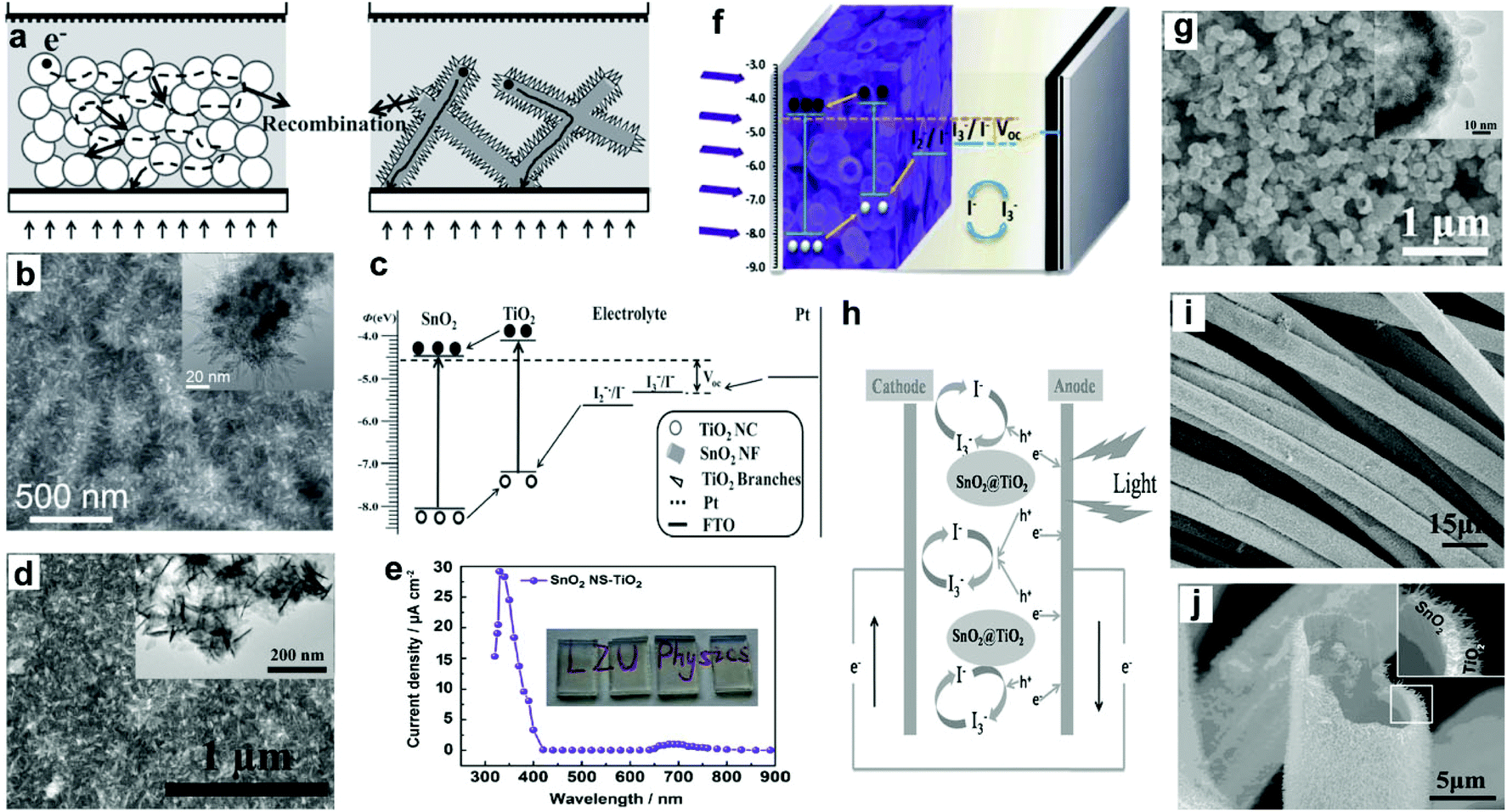 | ||
| Fig. 10 (a) Diagram of self-powered UV-PDs based on nc-TiO2 (left) and B-SnO2 NF films (right), (b) SEM image of B-SnO2-NF films, the inset is their TEM image, (c) energetics of operation of B-SnO2-NF UV-PD. (d) Top view image of SnO2 NS-TiO2 films, the inset is their TEM image, and (e) spectral response of the self-powered UV-PDs, the inset is the digital photograph of transparent SnO2 NS-TiO2 films. (f) Structure scheme of UV-PDs based on SnO2@TiO2 HNSs, (g) SEM images of SnO2@TiO2 hierarchical HNSs, the insets show the TEM image. (h) Detailed carrier transfer process of the PEC cell under illumination, (i) SEM images of SnO2 NP-TiO2 NR composites, (j) cross-sectional view SEM image of the SnO2@TiO2 microtube. (a–c) and (h–j) Reproduced from ref. 28 and 32, respectively. Copyright © 2012 and 2014 Wiley-VCH. (d and e) and (f and g) Reproduced from ref. 47 and 31, respectively. Copyright © 2014 Elsevier Ltd. | ||
3.4.3.1 NP/1D nanostructure hybrids. Compared to NPs, 1D NWs or NRs usually possess the advantages of a fast electron transport rate and excellent light scattering. However, at the same time, these two nanostructures suffer from their low SSA which usually results in a low light absorption efficiency and hence leads to low Jsc and Rλ.101,102 Zhang et al.52 assembled anodic TiO2 NTA/NP composites into photoanodes. Compared to the bare TNTAs, the TNTA/NP composites exhibit a visible-blind characteristic but with a slight red shift in the absorption edge. Moreover, this type of NTA/NP photoanode shows a fast photoresponse to UV light (200–400 nm), and the Jsc is increased by 29% compared to that of the bare TNTAs. These improvements in their PEC performances could be mainly due to the higher separation efficiency of the photogenerated electron–hole pairs and effective charge transport between the TiO2 NTs and NPs.
3.4.3.2 Reduced NRAs. Surficial reduction can greatly increase the donor density of oxide nanostructures, which can benefit the photogenerated carrier transport. Yao et al.103 prepared a type of hydrogenated ZnO hierarchical NRA (H-ZnO HNRA) by a two-step electrochemical process. After hydrogenation annealing, the color of the white ZnO HNRA film changes to black H-ZnO HNRAs. The carrier density of H-ZnO HNRAs is enhanced over 14 fold compared to that of the pristine ones, and H-ZnO HNRAs show a broad UV photoresponse from 300 to 370 nm with an IPCE of more than 90%. Similar results can also be seen in the study by Xu et al.60
Moreover, it is suggested that the existence of Ti3+ defects (oxygen vacancies) in bulky TiO2 nanostructures can enhance their electrical conductivity.104 In this case, Ti3+-induced mid-gap states, as shallow donor sites, could contribute to the charge density enhancement and narrowed band gap and could lead to further improvement in PEC efficiency.105 Zhang et al.106 reported the preparation of reduced TNTs (r-TNTs) using electrochemical doping via cathodic reduction. The r-TNTs show a visual change of color from grey to dark blue, and their charge transfer resistance decreases from 1246 to 90.79 Ω cm−2. And the Jp of r-TNTs increases by 33.3% compared to that of the pristine TNTs under UV irradiation (375 nm, 300 mW cm−2).
3.4.3.3 Element doping. Doping suitable elements into TiO2 is found to be important for the reduction of the photogenerated hole–electron recombination rate.107 Wang et al. fabricated nitrogen-doped TiO2 mesosponge (N-TMSE and N-TMSW) by transformation of TNTAs using a solvothermal method (Fig. 11a).57 The color of TNTAs changes from the original grey to sky-blue after doping with the N element, which corresponds to higher light absorption in the UVA region. Under UV irradiation (254 nm, 500 W) in a 0.1 M Na2SO4 electrolyte, the saturated Jp values of N-TMSE and N-TMSW are respectively ∼427 and 370 μA cm−2, which are much higher than those of the pristine TNTAs (318 μA cm−2). The improved Jp could be mainly because N doping facilitates the separation and transfer of photogenerated electron/hole pairs. Moreover, Xu et al.60 doped the Sn element into TiO2 NWs by a one-pot hydrothermal synthesis. The obtained Sn-doped TiO2 (Sn/TiO2) NWs with Sn/Ti ratios of 1–2% are single crystalline with a rutile structure. The Sn/TiO2-12 h NW photoanode shows a high Jp of 2.0 mA cm−2, which is enhanced 100% compared to the best pristine TiO2 NW photoanodes. This increase in photocurrent density is mainly ascribed to the enhancement of photoactivity in the UV region and the significant improvement in density of n-type carriers by Sn doping.
 | ||
| Fig. 11 (a) Transformation processes of NTs into mesosponge of TiO2 by solvothermal treatment in an ethanol solution of ammonia, and their corresponding optical and SEM images (top views). (b) Schematic illustration of the preparation of TiO2:(W, C) NWs by ex situ doping method; the cross-sectional SEM image is shown in the bottom, the inset shows TEM and EDX mapping images. (a) Reproduced from ref. 57. Copyright © 2012 Elsevier Ltd. (b) Reproduced from Cho et al.108 Copyright © 2013 Nature Publishing Group. | ||
Although a suitable mono-doping (single element doping) can enhance the PEC performance of TiO2 to some extent, excessive mono-doping will increase carrier recombination centers and reversely decreases the overall PEC performance. Then, a new type of donor–acceptor co-doping concept was proposed to improve the PEC performances of TiO2 photoanodes.109 This type of co-doping of TiO2 with donor–acceptor pairs can not only enhance the charge transport, but also reduce charged defects and their associated recombination, and accordingly improve their PEC performances. Dong's group reported a type of bimetallic Au–Pt NP/NH2-group functionalized TiO2 hybrid nanoparticles (denoted as f-TiO2–Au/Pt NPs) via a simple self-assembly approach.110 These f-TiO2–Au/Pt NPs consist of evenly dispersed Au/Pt NPs (6–7 nm) on f-TiO2 colloid spheres with a nanoporous surface. Under UV illumination (365 nm), the f-TiO2–Au/Pt NPs show a stable Ip of 0.30 ± 0.02 μA, which is about 4-fold that of the f-TiO2 NPs (0.08 ± 0.03 μA). Moreover, Cho et al. reported a novel ex situ method to co-dope TiO2 with W and C elements by sequentially annealing W-precursor-coated TiO2 NWs in carbon monoxide gas (Fig. 11b).108 The integrated UV light absorption (plus scattering) values of (W, C) co-doped TiO2 NWs is enhanced only 7.56% compared to that of the undoped ones, while the IPCE value of the co-doped TiO2:(W, C) NWs is ∼80% at 380 nm, which is enhanced 150% compared to that of the higher undoped TiO2 (∼32% at 395 nm). And the saturation Jp of the co-doped TiO2:(W, C) NWs is 2.4 times as high as that of the undoped TiO2 NWs. These enhancements suggest that co-doping with donor–acceptor pairs can greatly enhance charge separation and transport efficiency. Interestingly, the co-doped TiO2:(W, C) NWs also show very fast photoresponse to UV light.
3.4.3.4 Optics–electrics highways. Recently, conductive nanostructure modified technology has been employed as a promising way to boost the performances of PEC cells via optics–electrics highways.111–114 It has been applied to significantly accelerate the carriers’ transport and separation, and hence considered to be one of the most attractive technologies to improve the η. Dong et al.112 first proposed a concept of “optics–electrics highways” using a type of bristled silver NW@TiO2 core–shell nanostructures (Fig. 12a). It is demonstrated that these constructed composites significantly accelerate electron transport as well as reduce recombination, and then greatly improve the charge collection efficiency of the cells, and accordingly enhance the IPCE by 43%. However, this type of metal nanostructure can often generate localized surface plasmon resonance, which can not only enhance light harvesting in the UV region, but also greatly increase the photoresponse in the visible light region.
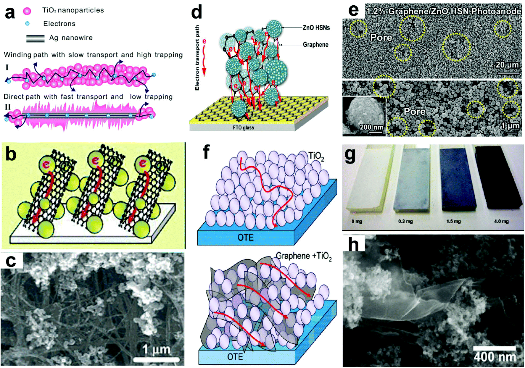 | ||
| Fig. 12 (a) Schematic diagram of photoelectrons transport in photoanodes of (I) pure and (II) Ag NW-modified TiO2. (b) Schematic illustrations of electron transport across SWCNT-doped TiO2 films, and (c) SEM images of SWCNT/TiO2 films. (d) Schematic diagram of the graphene/ZnO HSN composite photoanode and the possible electron transport path within the structure; and (e) top-view SEM images of graphene/ZnO HSN composites (∼1.2 wt% graphene loading), the inset is the magnified image of an individual ZnO HSN. (f) Schematic illustrations of electron transport in pristine TiO2 (upper) and r-GO–TiO2 (lower) nanocomposites, (g) photographs of TiO2 films with different r-GO loadings, and (h) SEM image of r-GO–TiO2 nanocomposites. (a) Reproduced from ref. 112. Copyright © 2014, Elsevier. (b and c), (d and e) and (g and h) Reproduced from ref. 58, 115 and 51, respectively. Copyright © 2007, 2013 and 2010 American Chemical Society. | ||
Carbon nanostructures, such as single-walled carbon nanotubes (SWCNTs), were also used as conducting scaffolds in TiO2-based PEC cells, in which TiO2 nanoparticles were dispersed on SWCNTs (Fig. 12b and c).58 Compared to the undoped TiO2 cells, the SWCNT/TiO2-based cells show a great increase (over 200%) in Jp and/or η values, indicating the beneficial role of the SWCNT as a conducting scaffold to facilitate charge transport in TiO2 films. Meanwhile, multi-walled carbon nanotubes (MWCNTs) were also incorporated into rutile TiO2 NWAs.55 It is found that on increasing the MWCNT content, the absorption edges of the TiO2@MWCNT NWA films are slightly blue-shifted with wavelength of ∼10 nm. And the maximum η was observed from the TiO2@MWCNT-0.1 NWA films, and it is enhanced 194% compared to that of the undoped ones. Further EIS results suggest that the small amount of MWCNT would promote the photogenerated electron transfer, and thus enhance the PEC performances of the devices. However, like mono-element doping, excessive MWCNT contents can also increase the trap state formation, and thus photogenerated electrons would spend more time to reach the FTO substrate.
Graphene is another type of carbon nanostructures that can also be used to enhance electron transport properties of oxide photoanodes. Compared to CNTs, reduced graphene oxide (r-GO) can provide a 2-D conductive support path for charge transport and collection at the electrode surface (Fig. 12f). In view of this point, Kamat's group synthesized a type of r-GO–TiO2 nanocomposite via a solution-based method involving photocatalytic reduction of GO.51 The color of TiO2 thin films gradually changes from white to black with increasing the addition of r-GO (Fig. 12g and h). The r-GO–TiO2 composites exhibit the maximum η value of 13.9% at ∼350 nm, which is enhanced 87.8% compared to that of the pure TiO2 films (7.4%). Upon UV irradiation (320–400 nm, 100 mW cm−2) in the 1 M KOH electrolyte, the r-GO–TiO2 films (with an r-GO of 0.05 mg cm−2) output a Jp of ∼38 μA cm−2, which is enhanced 90% compared to that of the TiO2 films (∼20 μA cm−2). These observed enhancements in the photocurrent and IPCE represent improved charge transport from r-GO–TiO2 nanocomposites to the collecting electrode surface. Similar results can also be seen in the study by Xu et al.,115 in which graphene was incorporated into ZnO nanoparticle photoanodes (Fig. 12d). After incorporating 1.2 wt% graphene into the 3 μm thick ZnO hierarchical structured nanoparticle (HSN) photoanode (Fig. 12e), the assembled devices exhibit a high Jsc of 10.89 mA cm−2 and an η of 3.19%, which are increased by 43.48% and 38.09%, respectively, compared to those of the devices without graphene. Moreover, it was also found that the incorporation of graphene into electrodes could not only effectively decrease the internal resistance within the photoanodes, but also markedly prolong electron lifetime and effective diffusion length. This allows the utilization of thicker photoanodes that could afford enhanced SSA for light harvesting, and an impressively high η of 5.86% was achieved for the 9 μm thick ZnO HSN photoanode. However, as in the case of MWCNTs, excessive r-GO loadings will adversely affect the electron transport in the composite films. And the incorporated graphene can cause more oxygen-related defects in the ZnO HSN photoanode, which often shows an enhanced visible light absorption.
3.5 Recent multi-functional PEC UV-PDs
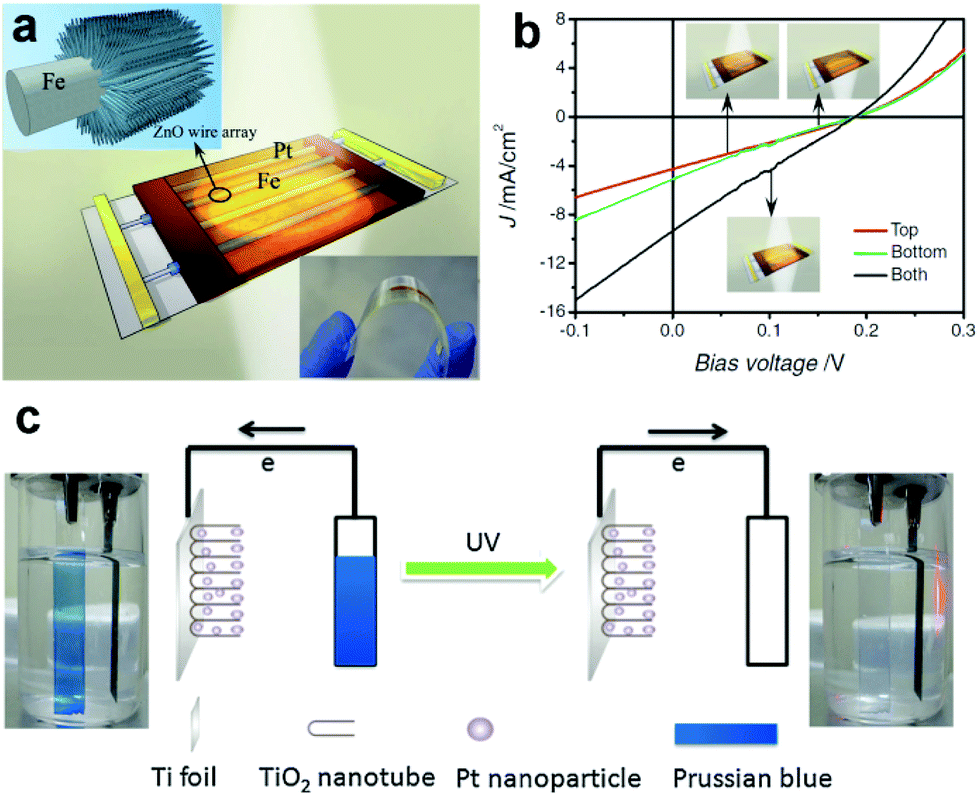 | ||
| Fig. 13 (a) Schematic prototype of double-sided transparent PEC devices. The left inset shows hierarchical ZnO-NWA/Fe microwires, and the right one shows the high flexibility of the device. (b) J–V curves of double-sided transparent cells under illumination from the top, bottom, and both sides. (c) General working principles of a self-powered, visual and self-recovered PD, the inset photographs show the color changes of the PB/ITO ON/OFF UV illumination. (a and b) Reproduced from ref. 116. Copyright © 2012 Wiley-VCH. (c) Reproduced from ref. 117. Copyright © The Royal Society of Chemistry 2014. | ||
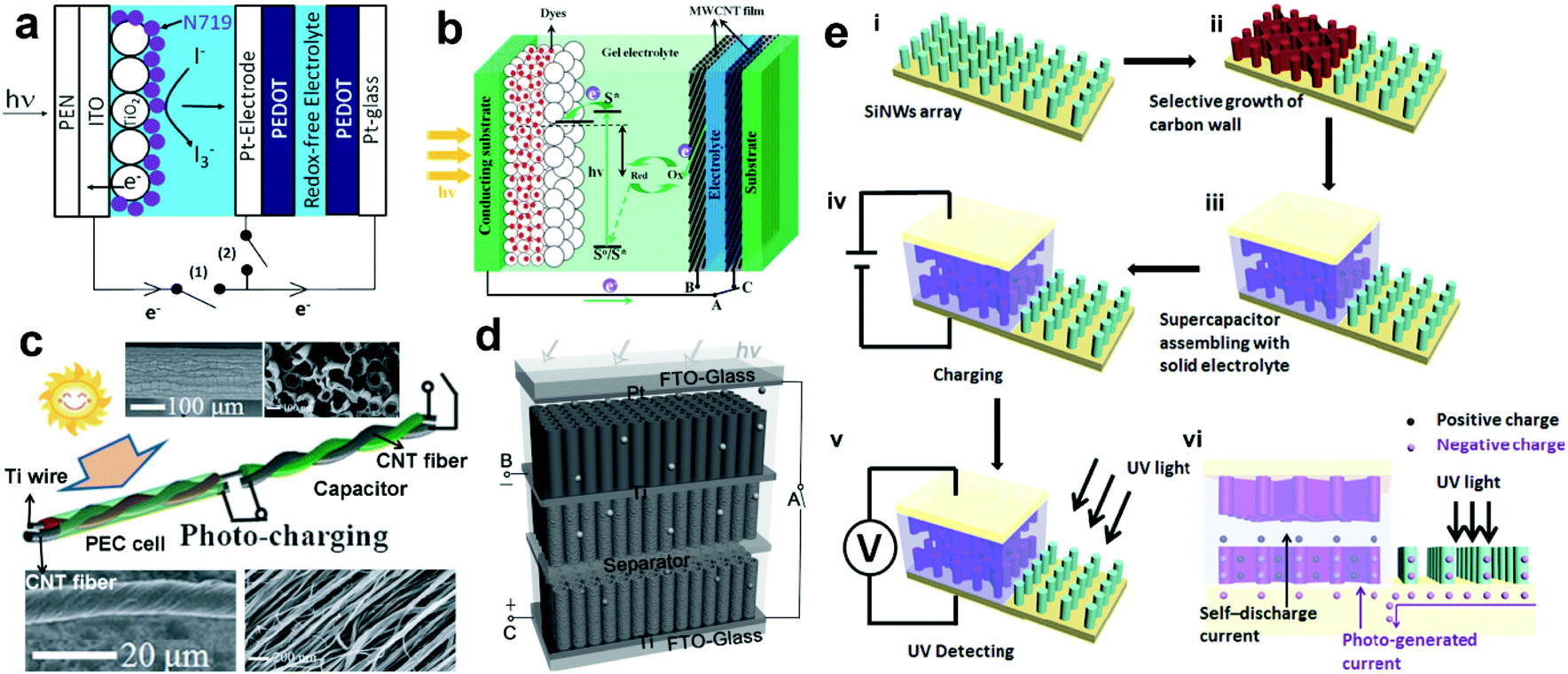 | ||
| Fig. 14 (a) Configuration of the optoelectronic device containing a DSSC and a polymer-based SC using a Pt wire as BPE. (b) Schematic illustration of a PEC cell/SC optoelectronic device using aligned MWCNT films as BPEs. (c) Schematic illustration of the wire-shaped device integrated with a PEC cell/SC optoelectronic device using a Ti wire as BPE. The upper insets show SEM images of a Ti wire coated with aligned TNTAs, and the lower insets show SEM images of a CNT fiber. (d) schematic illustration and work mechanism of a PEC cell/SC optoelectronic device using TNTAs as BPEs. (e) Fabrication process and structure of the bi-functional UV-PD. (a) Reproduced from ref. 118. Copyright © 2012 Elsevier Ltd. (b) Reproduced from ref. 120. Copyright © 2013 The Royal Society of Chemistry. (c and d) Reproduced from ref. 121 and 122, respectively. Copyright © 2012 and 2014 Wiley-VCH. (e) Reproduced from ref. 123. Copyright © 2015 Elsevier Ltd. | ||
More recently, Shen's group employed a BPE of TNAs into an optoelectronic integration.122 As shown in Fig. 14d, 1D anodic titanium oxide (ATO) NTAs were used as the photoanode materials for PEC cells and hydrogenated ATO (ATO-H) NTA as the cathode materials for electrochemical SCs. On visible light illumination, a pulsed anodic photocurrent of ∼2.6 mA cm−2 occurred promptly and then gradually decayed to 0.025 mA cm−2 in 1 s. Consequently, a maximum, stable and repeatable charge voltage of 0.61 V is achieved on SC after being photo-charged for 1 s. These results indicate that this type of optoelectronic device can also show a rapid response to light, even to UV light. In view of this, Zhang's group tried to integrate a UV-PD with a supercapacitor (SC) on one vertical-aligned silicon NW (SiNW) array electrode,123 in which carbon coated SiNWs were used as the electrode for the SC and the pristine SiNWs were used as the electrode for UV-PDs (Fig. 14e). The assembled SC shows a capacitance density of 13.6 F cm−3, which can be fully charged in 80–100 s and then support the UV-PDs for 10 h. Upon UV illumination (365 nm), the photoresponse can be observed from the external circuit potential increase (0.03–0.12 V) between the two electrodes of the SC. Although the reported UV detecting performances are not comparable to those from the above PEC UV-PDs, this type of self-powered multi-functional system that integrates power conversion/storage with UV light detection will open a new insight into the design of multi-functional PEC UV-PDs.
4 Summary and outlook
In this review, we have discussed the recent advances in self-powered PEC UV-PDs. Various nanostructures, including nc-films, NWs/NRs, NTs, NSs, NRAs, NTAs, nano-forest, etc., have been synthesized for photoanodes of PEC UV-PDs benefiting from their high UV light absorption, fast carrier separation/transport efficiencies, high spectral responsivity, high photosensitivity, and fast photoresponse. On the other hand, regarding the electrolyte, I−/I3−, water, Na2SO4 aqueous solution, etc., have been adopted, and the recently reported multi-functional PEC optoelectronic devices have been simply presented. However, current research work is still at the initial stage focusing on the design of photoanode structures. And these reviewed research studies are continuously developed according to the traditional optoelectronic devices (such as DSSC), involving device structure (sandwich structure), light harvesting, separation and transport mechanism of carriers, electrolytes, and counter electrodes. In nature, the mechanism for PEC UV-PDs is highly different from those for other optoelectronic devices. However, several issues, such as the light absorption mechanism under UV illumination, interfacial charge dynamics, and recombination mechanism of carriers, have not been investigated in detail. Thus, future endeavors are needed to achieve further improvement in the material and device designs, and photo detecting performances for practical applications. The related outlook points are listed below:4.1 Photoanode structures
Photoanode materials and structures are among the most important components of the whole PD, and greatly determine the light harvesting of a PEC cell. We can optimize the structures of photoanodes for PEC UV-PDs from the following aspects:(i) UV light absorption. Usually, one optoelectronic device requires a photoanode film with sufficient thickness to absorb light, which is dependent on the penetration depth of UV light. Excessive thickness of the film will result in the increase of diffusion length of photogenerated electrons. Thus, the optimized thickness of photoanode films is an important issue. On the other hand, light scattering can increase the light propagation length, which is an effective approach to improve the light harvesting efficiency. It is noted here that light scattering can also enhance the visible light absorption, which is unfavorable to the UV selectivity of a PD. Thus, we should modify the size of nanostructures according to the wavelength of the target UV light, in order to achieve an ideal scattering effect.
(ii) Separation of photogenerated carriers. Under excitation by UV light, the electrons in the semiconductor will transit from the VB to CB, leaving a hole in the VB, which is subsequently reduced by ions in the electrolyte. Thus, first, it is necessary to guarantee an adequate semiconductor/electrolyte interface area, i.e., for the efficient separation of carriers, thus requiring a large SSA for the nanostructures in photoanodes. Second, apart from a high SSA, photoanodes should also possess suitable pore size and porosity, which will benefit the diffusion of the electrolyte to the whole film. It is also worth noting here that the penetration depth of UV light in the semiconductor is about 2 μm, which is much less than that of visible light. Then the film thickness required by PEC UV-PD (1–2 μm) is far less than that of a DSSC (10 μm for P25). This is to say, compared to a DSSC, the PEC UV-PDs need a smaller pore size in a photoanode film to meet effective diffusion of the electrolyte. Third, different crystal planes of semiconductors and size distribution of nanostructures will also affect this PEC interfacial charge dynamics.70
(iii) Transport of electrons. Photogenerated carriers will be separated at the semiconductor/electrolyte interface, and the electrons that are injected into the CB of the semiconductor will diffuse through the photoanode to the collector. Then, the transport rate is the key factor to determine the efficiency of the electron collection and the response speed of a PD. It is demonstrated that 1D nanostructures with high crystallinity and high aspect ratio can provide a direct transmission channel for electrons, which can greatly reduce the electron recombination at the grain boundary during the transport.78,87,88 And it is reported that the PEC UV-PDs assembled using TiO2 NWAs with an aspect ratio of 150 show greatly improved performances in photo detection. However, so far, few reports can be seen on the PEC UV-PDs based on high-electron-mobility and high-aspect-ratio semiconductor nanostructure such as TiO2 or SnO2. Besides, it is widely reported that conductive nanomaterials, such as CNTs, graphene, or metal nanostructures, can work as optics–electrics highways to boost the performance of PEC cells. Then, we believe that these strategies can also be used to enhance the performances of PEC UV-PDs.
(iv) Reducing the recombination of photogenerated electrons. In a PEC UV-PD, the surface of the semiconductor nanomaterial can come into direct contact with the electrolyte, which usually makes the electrons that transit to the CB easily recombine with the electrolyte ions. The optics–electrics highways mentioned above can not only facilitate the transport of electrons, but also reduce the recombination of electrons. On the other hand, one more effective way is to make the semiconductor heterojunction (such as p–n junctions and Schottky junctions) and to form a type-II band structure, which can block electron recombination by the barrier. According to Fig. 2, many semiconductor heterojunctions, such as ZnO/ZnS, ZnO/NiO, SrTiO3/TiO2, etc., have a high potential for application in PEC UV-PDs.
In brief, for an ideal photoanode, it is important to balance these four aspects mentioned above into an integrated system, not just to prepare high-SSA nanostructures with amazing morphologies and structures.
4.2 Device configuration
At present, most of the reported PEC UV-PDs possess a sandwich device configuration similar to a DSSC, as shown in Fig. 15a. In this configuration, TCO glass (such as FTO and ITO) is used as a transparent conductive substrate, which supports the photoanode materials. Once the devices start working, the target light should enter from the side of the photoanode through the TCO glass, and then excite the semiconductor materials. However, not all UV light can transmit through TCO glass easily. According to our tests, as shown in Fig. 15b (black solid line), UV light with wavelength less than 300 nm cannot transmit through TCO glass, and the one with wavelength larger than 330 nm just remains only 38% in intensity after transmission. These facts will inevitably lead to a serious issue, i.e., most of the reported PEC UV-PDs exhibit a peak response with a full width at half maximum of about 40 nm in the range of 300–400 nm and a very low peak value in spectral responsivity at 330 nm, as shown in Fig. 15b (red solid line). If the filtering effect on the UV light source from the substrate material can be removed, the performances of PEC UV-PDs will be greatly improved. More interestingly, the response spectrum will broaden, showing an ideal response curve similar to the red dotted line shown in Fig. 15b. Thus, it is very urgent to solve this “UV-filtering” problem. Some potential approaches are summarized below:(i) To design a novel UV transparent conductive substrate to replace the traditional TCO glass. For instance, Bao et al. have prepared a type of transparent conductive substrate based on a metal NW mesh by in situ etching (Fig. 15c),124 which shows ∼90% transmittance within a ultra-wide wave range of 200–2000 nm and a very low resistance (2.2 Ω sq−1). Moreover, Cui's group prepared a metal NW mesh via the sputtering or evaporation method using electrospun NWs as templates (Fig. 15d), which shows a sheet resistance of ∼2 Ω sq−1 at 90% transmission.125 However, when applied to PEC UV-PDs, these new transparent conductive substrates will meet some troubles, i.e., how to well contact the semiconductor photoanode films with the conductive layer, and how to conduct a low-temperature sintering of semiconductor films because the melting point of metal NWs is usually very low.
(ii) Another effective approach is to design a type of planar device structure, i.e., put the semiconductor photoanode and counter electrode on the same substrate, which are separated via some special method such as interdigital electrode or fiber devices. And then the electrolyte will be perfused between them, and the light source can enter from the surface UV transparent window without any loss.
 | ||
| Fig. 15 (a) Schematic of UV light entering a PEC PD using FTO as electrode connectors. (b) Typical transmittance spectrum of FTO glass (black solid line), experimental spectral response of PEC UV-PDs (red solid line), and the ideal spectral response of a PEC UV-PD (red dotted line). (c) (left) Schematic in situ fabrication of a metal NW network via the ion beam etching process using a polymer NF network as the shadow mask, and (right) optical transmission spectra of flexible metal networks. (d) Schematic of the polymer-NF templating process for fabricating nanotroughs. (c) Reproduced from ref. 124. Copyright © 2015 American Chemical Society. (d) Reproduced from ref. 125. Copyright © 2013, Nature Publishing Group. | ||
4.3 Material/band-gap adjustable and deep-UV detectors
The newly-reported PEC UV-PDs are mainly based on the ZnO, TiO2 and SnO2, which have been widely used in PEC devices. However, there exist some drawbacks in those semiconductors, such as low electron mobility, poor stability and so on. Thus, it is of great importance to seek more alternative materials to promote the practical applications of PEC UV-PDs.(i) In fact, compared with other PEC applications such as DSSC, photocatalysis, photolysis of water, and so on, PEC UV-PDs usually show a low requirement in the crystal structure, absorptivity, and energy band position of the semiconductor nanomaterials. And many wide-band-gap semiconductor oxides, nitrides and sulfides can be selected for their photoanode materials. For instance, GaN possesses a wide band gap of 3.4 eV, a high electron mobility of 900 cm2 V−1 s−1, and a high UV radiation stability, which will make it show high potential for applications in PEC UV-PDs.126 Besides, many ternary inorganic compounds with a perovskite structure, such as SrTiO3 (3.15 eV), CaTiO3 (3.6 eV), and BaTiO3 (3.3 eV), shows excellent behavior in the field of DSSC, and it is believed that these materials might also play a good role in PEC UV-PDs.
(ii) For practical applications, it is often required that UV-PDs possess a tunable detecting cutoff wavelength, which can be realized by adjusting the semiconductors’ band gap. And this idea has been widely reported and realized in the photoconductors. For instance, some ternary alloy semiconductors such as ZnMgO,127 AlGaN,128 and so on show a good ability for band-gap modulation, and have successfully covered the wave range from 200 to 365 nm via the component ratios. However, few similar studies have focused on PEC UV-PDs up to now. And it is worth noting that the energy band structure of the semiconductor used in PEC UV-PDs should well match with the redox potential of the chosen electrolyte. In addition, the wetting property between the semiconductor and the used electrolyte is another important issue that can greatly influence the electrolyte ion diffusion, and thus determine the charge collecting efficiency.
(iii) Deep-UV detectors have many important applications in military, space, and other fields. At present, photoconductors/Schottky-type deep-UV detectors based on ultra-wide-band-gap semiconductors often exhibit a low performance. Thus, it is instructive and interesting for researchers to explore PEC deep-UV detectors.
4.4 Stabilities of PEC UV-PDs
Running stability is one important indicator of the practical applications of a device. Also the stability of PEC UV-PDs is an essential issue that we should pay attention to. However, few papers have reported a systematical study of the running stability of PEC UV-PDs. As is well known, compared to the solid UV-PDs based on photoconductance (p–n or Schottky junctions), PEC ones usually show a worse stability, which is mainly due to the volatilization of the electrolyte (depending on the packaging process), the corrosion and surface passivation of the semiconductor, the gas generation during the work process, the decreased catalytic ability of the counter electrode (such as Pt), and so on. Thus, in view of the above points, some future work should be conducted to improve the stability of PEC UV-PDs. For instance, Chen's group attempted a nanostructured quasi-solid-state UV-PD fabricated using a liquid LC-embedded I−/I3− electrolyte, and obtained improved light harvesting and stability.33 Further more research on improving the stabilities of UV-PDs is still on the way.4.5 Multi-functional PEC UV-PDs
Recent reports on flexible, visual, and multi-functional UV-PDs with BPEs have just given an initial attempt or proposed a prototype, and further development of multi-functional detectors will significantly broaden the application fields of PEC UV-PDs. On the other hand, compared to the PDs based on the metal–semiconductor–metal structure of bulky semiconductor materials, the PEC UV-PD is based on nanomaterials and an electrolyte system, thereby showing a great potential in flexible applications. As demonstrated, this new type of UV-PD can work in the electrolyte of “non-toxic, environmentally-friendly and cheap” water, which makes the devices safer to a large extent. Moreover, it is speculative that interval replacement and filling of the water electrolyte in the devices can easily realize their circular utilization. Therefore, in brief, those advantages of UV-PDs, including fast reponsibility, high reliability and environment protection properties, low-cost and self-powered system, and possible integration with other functional devices, will make them have great potential in various civilian application fields, such as medical and health protection, and wearable devices in the future.Acknowledgements
The authors acknowledge the financial support from the National Natural Science Foundation of China (Grant No. 51202100 and 61404065). The authors also thank the great contribution from Drs Xiaodong Li and Caitian Gao who have graduated from our group.References
- E. Monroy, F. Omnès and F. Calle, Semicond. Sci. Technol., 2003, 18, R33 CrossRef CAS.
- G. Shen and D. Chen, Recent Pat. Nanotechnol., 2010, 4, 20–31 CrossRef CAS PubMed.
- C. L. Hsu and S. J. Chang, Small, 2014, 10, 4562–4585 CrossRef CAS PubMed.
- Z. Alaie, S. Mohammad Nejad and M. H. Yousefi, Mater. Sci. Semicond. Process., 2015, 29, 16–55 CrossRef CAS.
- G. Konstantatos and E. H. Sargent, Nat. Nanotechnol., 2010, 5, 391–400 CrossRef CAS PubMed.
- J. Zou, Q. Zhang, K. Huang and N. Marzari, J. Phys. Chem. C, 2010, 114, 10725–10729 CAS.
- C. Soci, A. Zhang, B. Xiang, S. A. Dayeh, D. P. R. Aplin, J. Park, X. Y. Bao, Y. H. Lo and D. Wang, Nano Lett., 2007, 7, 1003–1009 CrossRef CAS PubMed.
- Y. Han, G. Wu, M. Wang and H. Chen, Polymer, 2010, 51, 3736–3743 CrossRef CAS.
- W. Tian, C. Zhang, T. Zhai, S. L. Li, X. Wang, M. Liao, K. Tsukagoshi, D. Golberg and Y. Bando, Chem. Commun., 2013, 49, 3739–3741 RSC.
- X. Wang, Z. Xie, H. Huang, Z. Liu, D. Chen and G. Shen, J. Mater. Chem., 2012, 22, 6845–6850 RSC.
- M. Gratzel, Nature, 2001, 414, 338–344 CrossRef CAS PubMed.
- C. Basant, P. Leela Srinivas, K. Salaru Baba and C. N. R. Rao, Jpn. J. Appl. Phys., 2011, 50, 100206 CrossRef.
- C. W. Litton, D. C. Reynolds, T. C. Collins, J. Zhong and Y. Lu, in Zinc Oxide Materials for Electronic and Optoelectronic Device Applications, ed. P. Capper, S. Kasap and A. Willoughby, Wiley, 2011, vol. 11, p. 363 Search PubMed.
- S. Sawyer and D. Shao, in Handbook of Nanomaterials Properties, ed. B. Bhushan, D. Luo, S. R. Schricker, W. Sigmund and S. Zauscher, Springer, Berlin, Heidelberg, 2014, pp. 1177–1198 Search PubMed.
- Y. Li, F. D. Valle, M. Simonnet, I. Yamada and J. J. Delaunay, Appl. Phys. Lett., 2009, 94, 023110 CrossRef.
- S. Liu, J. Ye, Y. Cao, Q. Shen, Z. Liu, L. Qi and X. Guo, Small, 2009, 5, 2371–2376 CrossRef CAS PubMed.
- F. Fang, J. Futter, A. Markwitz and J. Kennedy, Nanotechnology, 2009, 20, 245502 CrossRef CAS PubMed.
- W. W. J. Liu, S. Bai and Y. Qin, ACS Appl. Mater. Interfaces, 2011, 3, 4197–4200 Search PubMed.
- B. Liu, Z. Wang, Y. Dong, Y. Zhu, Y. Gong, S. Ran, Z. Liu, J. Xu, Z. Xie and D. Chen, et al. , J. Mater. Chem., 2012, 22, 9379–9384 RSC.
- Y. Q. Bie, Z. M. Liao, H. Z. Zhang, G. R. Li, Y. Ye, Y. B. Zhou, J. Xu, Z. X. Qin, L. Dai and D. P. Yu, Adv. Mater., 2011, 23, 649–653 CrossRef CAS PubMed.
- W. Jin, Y. Ye, L. Gan, B. Yu, P. Wu, Y. Dai, H. Meng, X. Guo and L. Dai, J. Mater. Chem., 2012, 22, 2863–2867 RSC.
- X. Li, C. Gao, H. Duan, B. Lu, X. Pan and E. Xie, Nano Energy, 2012, 1, 640–645 CrossRef CAS.
- Y. Q. Bie, Z. M. Liao, H. Z. Zhang, G. R. Li, Y. Ye, Y. B. Zhou, J. Xu, Z. X. Qin, L. Dai and D. P. Yu, Adv. Mater., 2011, 23, 649–653 CrossRef CAS PubMed.
- S. M. Hatch, J. Briscoe and S. Dunn, Adv. Mater., 2013, 25, 867–871 CrossRef CAS PubMed.
- Q. Yang, Y. Liu, Z. Li, Z. Yang, X. Wang and Z. L. Wang, Angew. Chem., Int. Ed., 2012, 124, 6549–6552 CrossRef.
- Z. Zhan, L. Zheng, Y. Pan, G. Sun and L. Li, J. Mater. Chem., 2012, 22, 2589–2595 RSC.
- X. Hu, B. Heng, X. Chen, B. Wang, D. Sun, Y. Sun, W. Zhou and Y. Tang, J. Power Sources, 2012, 217, 120–127 CrossRef CAS.
- X. Li, C. Gao, H. Duan, B. Lu, Y. Wang, L. Chen, Z. Zhang, X. Pan and E. Xie, Small, 2013, 9, 2005–2011 CrossRef CAS PubMed.
- C. Gao, X. Li, Y. Wang, L. Chen, X. Pan, Z. Zhang and E. Xie, J. Power Sources, 2013, 239, 458–465 CrossRef CAS.
- Q. Li, L. Wei, Y. Xie, K. Zhang, L. Liu, D. Zhu, J. Jiao, Y. Chen, S. Yan and G. Liu, et al. , Nanoscale Res. Lett., 2013, 8, 1–7 CrossRef PubMed.
- L. Chen, X. Li, Y. Wang, C. Gao, H. Zhang, B. Zhao, F. Teng, J. Zhou, Z. Zhang and X. Pan, et al. , J. Power Sources, 2014, 272, 886–894 CrossRef CAS.
- X. Hou, X. Wang, B. Liu, Q. Wang, Z. Wang, D. Chen and G. Shen, ChemElectroChem, 2014, 1, 108–115 CrossRef.
- Y. Xie, L. Wei, Q. Li, Y. Chen, H. Liu, S. Yan, J. Jiao, G. Liu and L. Mei, Nanoscale, 2014, 6, 9116–9121 RSC.
- Y. Xie, L. Wei, Q. Li, Y. Chen, S. Yan, J. Jiao, G. Liu and L. Mei, Nanotechnology, 2014, 25, 075202 CrossRef PubMed.
- Z. Wang, S. Ran, B. Liu, D. Chen and G. Shen, Nanoscale, 2012, 4, 3350–3358 RSC.
- Y. Xie, L. Wei, G. Wei, Q. Li, D. Wang, Y. Chen, S. Yan, G. Liu, L. Mei and J. Jiao, Nanoscale Res. Lett., 2013, 8, 188 CrossRef PubMed.
- J. Xing, H. Wei, E. J. Guo and F. Yang, J. Phys. D: Appl. Phys., 2011, 44, 375104 CrossRef.
- J.-K. Lee and M. Yang, Mater. Sci. Eng., B, 2011, 176, 1142–1160 CrossRef CAS.
- T. Majumder, J. J. L. Hmar, K. Debnath, N. Gogurla, J. N. Roy, S. K. Ray and S. P. Mondal, J. Appl. Phys., 2014, 116, 034311 CrossRef.
- O. Game, U. Singh, T. Kumari, A. Banpurkar and S. Ogale, Nanoscale, 2013, 6, 503–513 RSC.
- Y. Han, C. Fan, G. Wu, H. Z. Chen and M. Wang, J. Phys. Chem. C, 2011, 115, 13438–13445 CAS.
- P. Guo, J. Jiang, S. Shen and L. Guo, Int. J. Hydrogen Energy, 2013, 38, 13097–13103 CrossRef CAS.
- W. J. Lee and M. H. Hon, Appl. Phys. Lett., 2011, 99, 251102 CrossRef.
- C. Cao, C. Hu, X. Wang, S. Wang, Y. Tian and H. Zhang, Sens. Actuators, A, 2011, 156, 114–119 CrossRef CAS.
- Y. Wang, W. Han, B. Zhao, L. Chen, F. Teng, X. Li, C. Gao, J. Zhou and E. Xie, Sol. Energy Mater. Sol. Cells, 2015, 140, 376–381 CrossRef CAS.
- C. W. Kim, S. P. Suh, M. J. Choi, Y. S. Kang and Y. S. Kang, J. Mater. Chem. A, 2013, 1, 11820–11827 CAS.
- C. Gao, X. Li, X. Zhu, L. Chen, Y. Wang, F. Teng, Z. Zhang, H. Duan and E. Xie, J. Alloys Compd., 2014, 616, 510–515 CrossRef CAS.
- J. Halme, P. Vahermaa, K. Miettunen and P. Lund, Adv. Mater., 2010, 22, E210–E234 CrossRef CAS PubMed.
- J. Wu, Z. Lan, J. Lin, M. Huang, Y. Huang, L. Fan and G. Luo, Chem. Rev., 2015, 115, 2136–2173 CrossRef CAS PubMed.
- Z. Sun, L. Xu, W. Guo, B. Xu, S. Liu and F. Li, J. Phys. Chem. C, 2010, 114, 5211–5216 CAS.
- Y. H. Ng, I. V. Lightcap, K. Goodwin, M. Matsumura and P. V. Kamat, J. Phys. Chem. Lett., 2010, 1, 2222–2227 CrossRef CAS.
- Y. Zhang, X. Li, M. Feng, F. Zhou and J. Chen, Surf. Coat. Technol., 2010, 205, 2572–2577 CrossRef CAS.
- J. Lei, X. Li, W. Li, F. Sun, D. Lu and J. Yi, Int. J. Hydrogen Energy, 2011, 36, 8167–8172 CrossRef CAS.
- N. L. Tarwal, V. V. Shinde, A. S. Kamble, P. R. Jadhav, D. S. Patil, V. B. Patil and P. S. Patil, Appl. Surf. Sci., 2011, 257, 10789–10794 CrossRef CAS.
- M. Chang, L. Wu, X. Li and W. Xu, J. Mater. Sci. Technol., 2012, 28, 594–598 CAS.
- Y. Z. Su, K. Xiao, Z. J. Liao, Y. H. Zhong, N. Li, Y. B. Chen and Z. Q. Liu, Int. J. Hydrogen Energy, 2013, 38, 15019–15026 CrossRef CAS.
- Q. Wang, X. Yang, X. Wang, M. Huang and J. Hou, Electrochim. Acta, 2012, 62, 158–162 CrossRef CAS.
- A. Kongkanand, R. Martínez Domínguez and P. V. Kamat, Nano Lett., 2007, 7, 676–680 CrossRef CAS PubMed.
- Y. Li, H. Yu, W. Song, G. Li, B. Yi and Z. Shao, Int. J. Hydrogen Energy, 2011, 36, 14374–14380 CrossRef CAS.
- M. Xu, P. Da, H. Wu, D. Zhao and G. Zheng, Nano Lett., 2012, 12, 1503–1508 CrossRef CAS PubMed.
- W. Chen, Y. Qiu and S. Yang, Phys. Chem. Chem. Phys., 2012, 14, 10872–10881 RSC.
- P. Tiwana, P. Docampo, M. B. Johnston, H. J. Snaith and L. M. Herz, ACS Nano, 2011, 5, 5158–5166 CrossRef CAS PubMed.
- W. Dai, X. Pan, S. Chen, C. Chen, Z. Wen, H. Zhang and Z. Ye, J. Mater. Chem. C, 2014, 2, 4606–4614 RSC.
- S. Yang, Y. Hou, J. Xing, B. Zhang, F. Tian, X. H. Yang and H. G. Yang, Chem. – Eur. J., 2013, 19, 9366–9370 CrossRef CAS PubMed.
- J. Zhao, W. Zhang, E. Xie, Z. Liu, J. Feng and Z. Liu, Mater. Sci. Eng., B, 2011, 176, 932–936 CrossRef CAS.
- B. Liu, X. Zhao, C. Terashima, A. Fujishima and K. Nakata, Phys. Chem. Chem. Phys., 2014, 16, 8751–8760 RSC.
- T. Zhai, L. Li, X. Wang, X. Fang, Y. Bando and D. Golberg, Adv. Funct. Mater., 2010, 20, 4233–4248 CrossRef CAS.
- H. Xue, X. Kong, Z. Liu, C. Liu, J. Zhou, W. Chen, S. Ruan and Q. Xu, Appl. Phys. Lett., 2007, 90, 201118 CrossRef.
- J. M. Macak, H. Tsuchiya, L. Taveira, S. Aldabergerova and P. Schmuki, Angew. Chem., Int. Ed., 2005, 44, 7463–7465 CrossRef CAS PubMed.
- I. S. Cho, Z. Chen, A. J. Forman, D. R. Kim, P. M. Rao, T. F. Jaramillo and X. Zheng, Nano Lett., 2011, 11, 4978–4984 CrossRef CAS PubMed.
- W. Q. Wu, B. X. Lei, H. S. Rao, Y. F. Xu, Y. F. Wang, C. Y. Su and D. B. Kuang, Sci. Rep., 2013, 3, 1352 Search PubMed.
- W. Q. Wu, H. S. Rao, H. L. Feng, X. D. Guo, C. Y. Su and D. B. Kuang, J. Power Sources, 2014, 260, 6–11 CrossRef CAS.
- J. Xu, Z. Chen, J. A. Zapien, C. S. Lee and W. Zhang, Adv. Mater., 2014, 26, 5337–5367 CrossRef CAS PubMed.
- T. Zhai, L. Li, Y. Ma, M. Liao, X. Wang, X. Fang, J. Yao, Y. Bando and D. Golberg, Chem. Soc. Rev., 2011, 40, 2986–3004 RSC.
- Q. Zhang and G. Cao, Nano Today, 2011, 6, 91–109 CrossRef CAS.
- M. Law, L. E. Greene, J. C. Johnson, R. Saykally and P. Yang, Nat. Mater., 2005, 4, 455–459 CrossRef CAS PubMed.
- L. Li, T. Zhai, Y. Bando and D. Golberg, Nano Energy, 2012, 1, 91–106 CrossRef CAS.
- S. H. Ko, D. Lee, H. W. Kang, K. H. Nam, J. Y. Yeo, S. J. Hong, C. P. Grigoropoulos and H. J. Sung, Nano Lett., 2011, 11, 666–671 CrossRef CAS PubMed.
- M. J. Bierman and S. Jin, Energy Environ. Sci., 2009, 2, 1050 CAS.
- X. Sun, Q. Li, J. Jiang and Y. Mao, Nanoscale, 2014, 6, 8769–8780 RSC.
- C. Gao, X. Li, B. Lu, L. Chen, Y. Wang, F. Teng, J. Wang, Z. Zhang, X. Pan and E. Xie, Nanoscale, 2012, 4, 3475–3481 RSC.
- X. Hou, B. Liu, X. Wang, Z. Wang, Q. Wang, D. Chen and G. Shen, Nanoscale, 2013, 5, 7831–7837 RSC.
- J. C. Fu, J. L. Zhang, Y. Peng, C. H. Zhao, Y. M. He, Z. X. Zhang, X. J. Pan, N. J. Mellors and E. Q. Xie, Nanoscale, 2013, 5, 12551–12557 RSC.
- N. K. Elumalai, R. Jose, P. S. Archana, V. Chellappan and S. Ramakrishna, J. Phys. Chem. C, 2012, 116, 22112–22120 CAS.
- S. Mridha, M. Nandi, A. Bhaumik and D. Basak, Nanotechnology, 2008, 19, 275705 CrossRef CAS PubMed.
- B. Hu, Q. Tang, B. He, L. Lin and H. Chen, J. Power Sources, 2014, 267, 445–451 CrossRef CAS.
- L. Chen, X. Li, L. Qu, C. Gao, Y. Wang, F. Teng, Z. Zhang, X. Pan and E. Xie, J. Alloys Compd., 2014, 586, 766–772 CrossRef CAS.
- C. Xu, J. Wu, U. V. Desai and D. Gao, J. Am. Chem. Soc., 2011, 133, 8122–8125 CrossRef CAS PubMed.
- Z. Wang, H. Wang, B. Liu, W. Qiu, J. Zhang, S. Ran, H. Huang, J. Xu, H. Han and D. Chen, et al. , ACS Nano, 2011, 5, 8412–8419 CrossRef CAS PubMed.
- Y. Hu, X. Yan, X. Chen, Z. Bai, Z. Kang, F. Long and Y. Zhang, Appl. Surf. Sci., 2015, 339, 122–127 CrossRef CAS.
- R. S. Selinsky, Q. Ding, M. S. Faber, J. C. Wright and S. Jin, Chem. Soc. Rev., 2013, 42, 2963–2985 RSC.
- S. Hernández, V. Cauda, D. Hidalgo, V. Farías Rivera, D. Manfredi, A. Chiodoni and F. C. Pirri, J. Alloys Compd., 2014, 615, S530–S537 CrossRef.
- M. Wang, C. Huang, Y. Cao, Q. Yu, Z. Deng, Y. Liu, Z. Huang, J. Huang, Q. Huang and W. Guo, et al. , J. Phys. D: Appl. Phys., 2009, 42, 155104 CrossRef.
- M. Wang, Y. Wang and J. Li, Chem. Commun., 2011, 47, 11246 RSC.
- S. Panigrahi and D. Basak, Nanoscale, 2011, 3, 2336–2341 RSC.
- S. H. Ahn, D. J. Kim, W. S. Chi and J. H. Kim, Adv. Mater., 2013, 25, 4893–4897 CrossRef CAS PubMed.
- U. V. Desai, C. Xu, J. Wu and D. Gao, J. Phys. Chem. C, 2013, 117, 3232–3239 CAS.
- C. Gao, X. Li, X. Zhu, L. Chen, Z. Zhang, Y. Wang, Z. Zhang, H. Duan and E. Xie, J. Power Sources, 2014, 264, 15–21 CrossRef CAS.
- J. Qian, P. Liu, Y. Xiao, Y. Jiang, Y. Cao, X. Ai and H. Yang, Adv. Mater., 2009, 21, 3663–3667 CrossRef CAS.
- A. Thapa, J. Zai, H. Elbohy, P. Poudel, N. Adhikari, X. Qian and Q. Qiao, Nano Res., 2014, 7, 1154–1163 CrossRef CAS.
- W. P. Liao and J. J. Wu, J. Mater. Chem., 2011, 21, 9255 RSC.
- Y. F. Wang, K. N. Li, W. Q. Wu, Y. F. Xu, H. Y. Chen, C. Y. Su and D. B. Kuang, RSC Adv., 2013, 3, 13804–13810 RSC.
- C. Yao, B. Wei, H. Ma, H. li, L. Meng, X. Zhang and Q. Gong, J. Power Sources, 2013, 237, 295–299 CrossRef CAS.
- F. Zuo, L. Wang, T. Wu, Z. Zhang, D. Borchardt and P. Feng, J. Am. Chem. Soc., 2010, 132, 11856–11857 CrossRef CAS PubMed.
- X. Zhang, H. Tian, X. Wang, G. Xue, Z. Tian, J. Zhang, S. Yuan, T. Yu and Z. Zou, Mater. Lett., 2013, 100, 51–53 CrossRef CAS.
- Q. Zhang, L. Wang, J. Feng, H. Xu and W. Yan, Phys. Chem. Chem. Phys., 2014, 16, 23431–23439 RSC.
- I. Justicia, P. Ordejón, G. Canto, J. L. Mozos, J. Fraxedas, G. A. Battiston, R. Gerbasi and A. Figueras, Adv. Mater., 2002, 14, 1399–1402 CrossRef CAS.
- I. S. Cho, C. H. Lee, Y. Feng, M. Logar, P. M. Rao, L. Cai, D. R. Kim, R. Sinclair and X. Zheng, Nat. Commun., 2013, 4, 1723 CrossRef PubMed.
- Y. Gai, J. Li, S. S. Li, J. B. Xia and S. H. Wei, Phys. Rev. Lett., 2009, 102, 036402 CrossRef PubMed.
- D. Wen, S. Guo, Y. Wang and S. Dong, Langmuir, 2010, 26, 11401–11406 CrossRef CAS PubMed.
- Y. C. Pu, G. Wang, K. D. Chang, Y. Ling, Y. K. Lin, B. C. Fitzmorris, C. M. Liu, X. Lu, Y. Tong and J. Z. Zhang, et al. , Nano Lett., 2013, 13, 3817–3823 CrossRef CAS PubMed.
- H. Dong, Z. Wu, F. Lu, Y. Gao, A. El-Shafei, B. Jiao, S. Ning and X. Hou, Nano Energy, 2014, 10, 181–191 CrossRef CAS.
- F. Teng, G. Zhang, Y. Wang, C. Gao, L. Chen, P. Zhang, Z. Zhang and E. Xie, Appl. Surf. Sci., 2014, 320, 703–709 CrossRef CAS.
- X. An, F. Teng, Z. Zhang, X. Pan, J. Zhou and E. Xie, Electron. Mater. Lett., 2014, 10, 95–99 CrossRef CAS.
- F. Xu, J. Chen, X. Wu, Y. Zhang, Y. Wang, J. Sun, H. Bi, W. Lei, Y. Ni and L. Sun, J. Phys. Chem. C, 2013, 117, 8619–8627 CAS.
- W. Wang, Q. Zhao, H. Li, H. Wu, D. Zou and D. Yu, Adv. Funct. Mater., 2012, 22, 2775–2782 CrossRef CAS.
- L. Han, L. Bai and S. Dong, Chem. Commun., 2014, 50, 802–804 RSC.
- H. W. Chen, C. Y. Hsu, J. G. Chen, K. M. Lee, C. C. Wang, K. C. Huang and K. C. Ho, J. Power Sources, 2010, 195, 6225–6231 CrossRef CAS.
- T. Miyasaka and T. N. Murakami, Appl. Phys. Lett., 2004, 85, 3932–3934 CrossRef CAS.
- Z. Yang, L. Li, Y. Luo, R. He, L. Qiu, H. Lin and H. Peng, J. Mater. Chem. A, 2013, 1, 954–958 CAS.
- T. Chen, L. Qiu, Z. Yang, Z. Cai, J. Ren, H. Li, H. Lin, X. Sun and H. Peng, Angew. Chem., Int. Ed., 2012, 51, 11977–11980 CrossRef CAS PubMed.
- J. Xu, H. Wu, L. Lu, S.-F. Leung, D. Chen, X. Chen, Z. Fan, G. Shen and D. Li, Adv. Funct. Mater., 2014, 24, 1840–1846 CrossRef CAS.
- L. Sun, X. Wang, K. Zhang, J. Zou, Z. Yan, X. Hu and Q. Zhang, Nano Energy, 2015, 15, 445–452 CrossRef CAS.
- C. Bao, J. Yang, H. Gao, F. Li, Y. Yao, B. Yang, G. Fu, X. Zhou, T. Yu and Y. Qin, et al. , ACS Nano, 2015, 9, 2502–2509 CrossRef CAS PubMed.
- H. Wu, D. Kong, Z. Ruan, P.-C. Hsu, S. Wang, Z. Yu, T. J. Carney, L. Hu, S. Fan and Y. Cui, Nat. Nanotechnol., 2013, 8, 421–425 CrossRef CAS PubMed.
- M. Zhang, Y. Wang, F. Teng, L. Chen, J. Li, J. Zhou, X. Pan and E. Xie, Mater. Lett., 2016, 162, 117–120 CrossRef CAS.
- K. Yudai, K. Toshiyuki, N. Hiroyuki and F. Shizuo, Jpn. J. Appl. Phys., 2006, 45, L857 CrossRef.
- A. Osinsky, S. Gangopadhyay, B. W. Lim, M. Z. Anwar, M. A. Khan, D. V. Kuksenkov and H. Temkin, Appl. Phys. Lett., 1998, 72, 742–744 CrossRef CAS.
Footnote |
| † These authors contributed equally to this work. |
| This journal is © The Royal Society of Chemistry 2016 |