
 Open Access Article
 This Open Access Article is licensed under a Creative Commons Attribution-Non Commercial 3.0 Unported Licence
Direct observation of the core/double-shell architecture of intense dual-mode luminescent tetragonal bipyramidal nanophosphors†
Su Yeon
Kim‡
a,
Jong Seok
Jeong‡
b,
K. Andre
Mkhoyan
b and
Ho Seong
Jang
*ac
aMaterials Architecturing Research Center, Korea Institute of Science and Technology, Hwarangno 14-gil 5, Seongbuk-gu, Seoul 136-791, Republic of Korea. E-mail: msekorea@kist.re.kr
bDepartment of Chemical Engineering and Materials Science, University of Minnesota, Minneapolis, MN 55455, USA
cDepartment of Nanomaterials Science and Engineering, Korea University of Science and Technology, Daejeon 305-350, Republic of Korea
First published on 8th December 2015
Abstract
Highly efficient downconversion (DC) green-emitting LiYF4:Ce,Tb nanophosphors have been synthesized for bright dual-mode upconversion (UC) and DC green-emitting core/double-shell (C/D-S) nanophosphors—Li(Gd,Y)F4:Yb(18%),Er(2%)/LiYF4:Ce(15%),Tb(15%)/LiYF4—and the C/D-S structure has been proved by extensive scanning transmission electron microscopy (STEM) analysis. Colloidal LiYF4:Ce,Tb nanophosphors with a tetragonal bipyramidal shape are synthesized for the first time and they show intense DC green light via energy transfer from Ce3+ to Tb3+ under illumination with ultraviolet (UV) light. The LiYF4:Ce,Tb nanophosphors show 65 times higher photoluminescence intensity than LiYF4:Tb nanophosphors under illumination with UV light and the LiYF4:Ce,Tb is adapted into a luminescent shell of the tetragonal bipyramidal C/D-S nanophosphors. The formation of the DC shell on the core significantly enhances UC luminescence from the UC core under irradiation of near infrared light and concurrently generates DC luminescence from the core/shell nanophosphors under UV light. Coating with an inert inorganic shell further enhances the UC–DC dual-mode luminescence by suppressing the surface quenching effect. The C/D-S nanophosphors show 3.8% UC quantum efficiency (QE) at 239 W cm−2 and 73.0 ± 0.1% DC QE. The designed C/D-S architecture in tetragonal bipyramidal nanophosphors is rigorously verified by an energy dispersive X-ray spectroscopy (EDX) analysis, with the assistance of line profile simulation, using an aberration-corrected scanning transmission electron microscope equipped with a high-efficiency EDX. The feasibility of these C/D-S nanophosphors for transparent display devices is also considered.
1. Introduction
Lanthanide (Ln) ion-doped inorganic nanocrystals (NCs), called nanophosphors, have been spotlighted due to their unique optical properties including sharp peak emission (peak width <10 nm), long lifetime, large Stokes/anti-Stokes shift, high photostability, and non-blinking luminescence.1–13 Unlike conventional bulk powder phosphors which usually exhibit either downconversion luminescence (DCL) with quantum cutting and downshifting, or upconversion luminescence (UCL), nanophosphors can emit both DCL and UCL simultaneously from a single particle.14,15 There is no difference in the 4f energy levels of Ln ions between nanocrystals and bulk crystals since the 4f electrons are well sheltered by the outer 5d orbitals, which make the 4f energy levels of Ln ions insensitive to environment and their sizes.16 Thus, bulk phosphors can also emit UC–DC dual-mode luminescence. However, since bulk (or powder) phosphors are usually synthesized by a conventional solid-state reaction method, doped activator ions are randomly distributed in the host crystals and increasing the dopant concentration to dope both UC- and DC-emitting activator ions into the host crystal may deteriorate the luminescence intensity.15 In nanophosphors, in contrast, Ln ions can be locally confined by constructing either a core/shell (C/S) structure or a large particle composed of smaller UC- and DC-emitting nanoparticles, which prevents deleterious cross-relaxations between dopant ions.14,15 Liu et al.15 reported such an approach showing dual-mode luminescence in NaGdF4:Yb,Tm/NaGdF4:Eu C/S nanophosphors even though intense luminescence was hardly achieved due to surface quenching effects17 because both DCL and UCL are emitted from the activator Eu3+ ions in the shell. In a further improved way, our previous study showed that single-particle dual-mode luminescence can be realized via a C/S architecture in which DC- and UC-emitting activators are separately doped into the core and the shell, and vice versa.18 In either case, however, activator ions in the shell suffer deterioration of their luminescence due to surface quenching by surface defects, ligands, and solvents.17,19 Thus, to achieve intense dual-mode luminescence, the surface quenching should be effectively suppressed. Additionally, new phosphor compositions showing high luminescence efficiency still need to be explored because the phosphor with higher luminescence efficiency exhibits brighter luminescence even with surface quenching. Here, we report for the first time colloidal Ce3+ and Tb3+ doubly-doped LiYF4 (LiYF4:Ce,Tb) nanophosphors with a single tetragonal phase exhibiting bright green light under ultraviolet (UV) light excitation. LiYF4 has a tetragonal scheelite structure whose compounds are well-known luminescent materials and bulk Li(Y,Gd)F4:Ce,Tb has been reported.20 In the nanometer scale, LiYF4:Eu/LiYF4:Ce,Tb C/S NCs (as well as the inverted system) were briefly discussed only in a point of view of Eu3+ emission enhancement.21 Nevertheless, much remains to be understood regarding the structural and luminescent properties of LiYF4:Ce,Tb in a nanophosphor system. The LiYF4:Ce,Tb nanophosphors showed approximately 20 times higher photoluminescence (PL) intensity than NaYF4:Ce,Tb nanophosphors5 which are known as one of the most efficient DC nanophosphors (DCNPs). When this bright green-emitting LiYF4:Ce,Tb is coated on the intense green-emitting Li(Gd,Y)F4:Yb,Er UC nanophosphors (UCNPs),3 bright dual-mode green luminescence can be realized from a single UC/DC C/S nanophosphor.18 Moreover, surface coating with an optically inert inorganic shell (IS) on the UC/DC nanophosphors further enhances DCL from the LiYF4:Ce,Tb DC shell by suppressing surface quenching.22 It is also noteworthy here that because controlling the optical functionality of a single nanoparticle can be achieved by designing materials with either core/double-shell (C/D-S) or C/S structures,22,23 detailed characterization of the designed structures providing direct information on the shell thickness and dopant distribution is essential. Previously, the C/S structures have been investigated on other nanophosphor systems, such as the NaYF4/NaGdF4,24,25 NaYF4:Yb,Er/NaGdF4,26 and NaGdF4:Yb,Tm/NaGdF4:X (X = Eu and Tb).23,27 Recently, NaYbF4:Nd/Na(Yb,Gd)F4:Er/NaGdF4 nanophosphors were also reported.28 Although the chemical composition of NaYF4 appears similar to LiYF4, they are quite different as they have different crystal structures; NaYF4 (or NaGdF4) has a cubic or hexagonal structure and LiYF4 has a tetragonal structure, which causes different morphologies. Recently, LiYF4:Yb,Er/Tm-based UCNPs were reported.29,30 Nonetheless, it should be noted that there is no report on LiYF4-based UCNPs with a C/S structure. Furthermore, detailed investigations on C/D-S nanophosphors with non-spherical faceted morphologies have not yet been reported.In this study, we report the luminescent properties of colloidal LiYF4:Ce,Tb DCNPs and highly bright dual-mode green-emitting tetragonal bipyramidal Li(Gd,Y)F4:Yb,Er/LiYF4:Ce,Tb/LiYF4 nanophosphors with a UC/DC/IS C/D-S architecture. The structure of the nanophosphors is determined by aberration-corrected scanning transmission electron microscopy (STEM) equipped with a high-efficiency energy dispersive X-ray spectroscopy (EDX) system in spite of the tetragonal bipyramidal shape of the nanophosphors and the absence of unique elements present in any one of the shells. The C/D-S structure of the nanophosphors was strictly verified by comparing the measured STEM-EDX profiles with the simulated ones.
2. Experimental
2.1. Materials
LiOH·H2O (99.995%), GdCl3·6H2O (99%), YCl3·6H2O (99.99%), CeCl3·7H2O (99.999%), TbCl3·6H2O (99.9%), YbCl3·6H2O (99.9%), ErCl3·6H2O (99.9%), NH4F (99.99+%), oleic acid (OA, technical grade 90%), and 1-octadecene (ODE, technical grade 90%) were purchased from Aldrich and they were used without further purification. Sodium oleate (>97%) was obtained from TCI.2.2. Synthesis of the LiYF4:Ce,Tb DCNPs
For the synthesis of colloidal LiYF4:Ce,Tb DCNPs, 1 mmol of Ln(oleate)3 (Ln = Y (70%), Ce (15%), and Tb (15%)) was prepared by adapting the previously reported method by Park et al.31 A three-necked flask was loaded with Ln(oleate)3, 10.5 ml OA, and 10.5 ml ODE followed by heating to 150 °C for 40 min. After the reaction mixture cooled to 50 °C, 10 ml of methanol (MeOH) solution containing LiOH·H2O (2.5 mmol) and NH4F (4 mmol) was added to the reaction solution. After stirring at 50 °C for 40 min, MeOH was removed and the solution was heated to 320 °C for 90 min under an Ar atmosphere. The synthesized DCNPs were dispersed in 10 ml chloroform after several washings with ethanol (EtOH).2.3. Synthesis of the Li(Gd,Y)F4:Yb,Er UCNPs
The Li(Gd,Y)F4:Yb,Er UCNPs were synthesized with a procedure similar to the synthesis of the LiYF4:Ce,Tb DCNPs. One mmol of Ln(oleate)3 (Ln = Gd (35%), Y (45%), Yb (18%), and Er (2%)) was used as Gd, Y, Yb, and Er precursors and other procedures were the same as those for the DCNP synthesis. The synthesized UC core was separately dispersed in 10 ml chloroform after several washings with EtOH.2.4. Synthesis of the Li(Gd,Y)F4:Yb,Er/LiYF4:Ce,Tb C/S nanophosphors
To synthesize UC/DC C/S nanophosphors, YCl3·6H2O (0.7 mmol), CeCl3·7H2O (0.15 mmol), and TbCl3·6H2O (0.15 mmol) were dissolved in 10.5 ml OA and 10.5 ml ODE by heat-treatment at 150 °C for 40 min. After cooling to 80 °C, 10 ml Li(Gd,Y)F4:Yb,Er UC core chloroform solution was injected to the reaction solution, and then 10 ml of MeOH solution containing LiOH·H2O (2.5 mmol) and NH4F (4 mmol) was added to the reaction solution. After 40 min stirring at 50 °C, MeOH was removed and the solution was heated to 300 °C for 110 min under an Ar atmosphere. The UC/DC C/S nanophosphors were then dispersed in 10 ml chloroform after washing with EtOH.2.5. Synthesis of the Li(Gd,Y)F4:Yb,Er/LiYF4:Ce,Tb/LiYF4 C/D-S nanophosphors
In the next step, the UC/DC/IS C/D-S nanophosphors were synthesized by uniformly coating a thin LiYF4 layer on the UC/DC C/S nanophosphors. One mmol of YCl3·6H2O was dissolved in 10.5 ml OA and 10.5 ml ODE by heat-treatment at 150 °C for 40 min before cooling to 80 °C and then Li(Gd,Y)F4:Yb,Er/LiYF4:Ce,Tb UC/DC C/S chloroform solution was injected to the reaction solution. Other procedures were the same as those for the C/S nanophosphor synthesis. The synthesized UC/DC/IS C/D-S nanophosphors were then dispersed in 10 ml chloroform after washing with EtOH.2.6. Preparation of the C/D-S nanophosphor–PDMS composites
The UC/DC/IS C/D-S nanophosphor–polydimethylsiloxane (PDMS) composites were prepared by mixing 10 ml of SYLGARD silicone elastomer 184 with 0.4 ml of the C/D-S nanophosphor solution (approximately 2 wt%) followed by the addition of a curing agent (1 ml). Finally, the C/D-S nanophosphor–PDMS composites were aged overnight and heat-treated at 80 °C for 1 h.2.7. Characterization
All PL spectra were collected using a Hitachi F-7000 spectrophotometer coupled to a continuous wave near infrared (NIR) laser (λ = 980 nm). PL decay profiles were obtained using an Edinburgh FL920 spectrometer. The absolute UC quantum efficiency (QE) was measured by using a barium sulfate coated integrating sphere and a spectrometer (OSA2000(OEM), PSITD-ETMAX Co. Ltd, Korea) equipped with a charge-coupled device (CCD) detector (Hamamatsu S10420, Back-thinned, 2D type). The DC QE of the C/D-S NPs was measured by using a Hamamatsu absolute PL quantum yield measurement system (C9920-02). The crystal structures of the synthesized nanophosphors were determined by X-ray diffraction (XRD) using a Bruker D8 ADVANCE diffractometer with Cu Kα radiation at 40 kV and 40 mA. Scanning electron microscopy (SEM) images were obtained using an FEI Nova nanoSEM operated at 10 kV. Conventional transmission electron microscopy (TEM) images were obtained using an FEI Tecnai G2 F20 (S)TEM operated at 200 kV. High-angle annular dark-field (HAADF) STEM imaging and STEM-EDX experiments were performed using an aberration-corrected FEI Titan G2 60-300 (S)TEM, operated at 80 kV. HAADF-STEM imaging and EDX experiments were conducted using a convergence semi-angle of ∼21 mrad to form the incident STEM probe and a collection semi-angle of approximately 55–200 mrad to collect electrons with the HAADF detector. EDX line profiles and spectrum images were obtained using a Super-X system, a quad-silicon drift detector (SDD) and a windowless in-polepiece EDX detector.32 The beam current was in the range of 100–250 pA. The electron beam probe dwell time and beam current were chosen to minimize beam damage during EDX experiments. However, slight beam damage was permitted to ensure sufficient X-ray signals.3. Results and discussion
Based on our previous study,18 the UC core and DC shell structure are more desirable than the DC core and UC shell structure for achieving bright dual-mode luminescent nanophosphors. As illustrated in Fig. 1, UCL can be enhanced by growing an inorganic inert shell on a UC core. When an inert shell is doped with activator ions such as Tb3+ ions, the shell exhibits DCL under UV light excitation. However, since the activators in the shell are close to the surface, it is highly probable that DCL from the DC shell will be weakened by the surface quenching compared with the corresponding colloidal DCNPs. Similar to enhancement of UCL, coating an inert shell on the DC shell enhances the DCL by suppressing the surface quenching. Since dopant ions in the shell are close to the surface of the nanophosphors, a strongly luminescent phosphor composition is also required for shell material.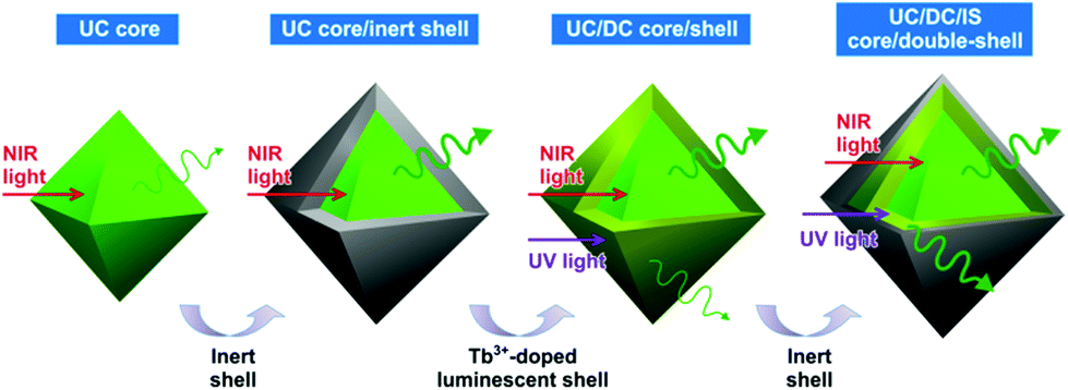 | ||
| Fig. 1 Schematic illustration showing step-by-step procedures to produce a bright dual-mode luminescent UC/DC/IS C/D-S nanophosphor. | ||
We found that colloidal LiYF4:Ce,Tb nanophosphors emit bright green emission and characterization of LiYF4:Ce,Tb nanophosphors is first demonstrated here. Colloidal LiYF4:Ce,Tb nanophosphors with a uniform size and shape were synthesized via a solution chemical route as described above. The XRD pattern of the LiYF4:Ce,Tb confirms that it has a single tetragonal phase without any second-phase impurities (Fig. S1†). The LiYF4:Ce,Tb DCNPs had a {112}-bound tetragonal bipyramidal morphology with sides of 32 ± 1 nm × 33 ± 1 nm (based on analysis of 200 nanoparticles), as shown in TEM and SEM images (Fig. 2a–c and S2†). The tetragonal bipyramidal shape can be directly attributed to the tetragonal structure of the LiYF4 host crystal (Fig. 2a). When the nanophosphor is aligned along the <22![[1 with combining macron]](https://www.rsc.org/images/entities/char_0031_0304.gif) > direction, which means one of the {112} facets sits on the TEM grid surface (note that this case is most commonly observed in the experiments), they appear to be hexagons in the TEM image (Fig. 2b). The {112}-bound tetragonal bipyramid is close to an octahedron (Fig. 2a and S2†). When the nanophosphors are viewed along the <110> and <021> directions, they appear to be diamond-shaped as shown in Fig. 2c. The high-resolution TEM (HR-TEM) images indicate that the as-synthesized LiYF4:Ce,Tb DCNPs are single-crystalline. The estimated d-spacings of 0.54 and 0.30 nm between the two adjacent lattice fringes are in good agreement with the d-spacings of the (002) and (112) planes of LiYF4 of 0.537 and 0.302 nm, confirming that the nanocrystal has a tetragonal structure (Fig. 2c and S3†). The SEM images also confirm the uniformity in size and the tetragonal bipyramidal morphology of LiYF4:Ce,Tb DCNPs (Fig. S2†).
> direction, which means one of the {112} facets sits on the TEM grid surface (note that this case is most commonly observed in the experiments), they appear to be hexagons in the TEM image (Fig. 2b). The {112}-bound tetragonal bipyramid is close to an octahedron (Fig. 2a and S2†). When the nanophosphors are viewed along the <110> and <021> directions, they appear to be diamond-shaped as shown in Fig. 2c. The high-resolution TEM (HR-TEM) images indicate that the as-synthesized LiYF4:Ce,Tb DCNPs are single-crystalline. The estimated d-spacings of 0.54 and 0.30 nm between the two adjacent lattice fringes are in good agreement with the d-spacings of the (002) and (112) planes of LiYF4 of 0.537 and 0.302 nm, confirming that the nanocrystal has a tetragonal structure (Fig. 2c and S3†). The SEM images also confirm the uniformity in size and the tetragonal bipyramidal morphology of LiYF4:Ce,Tb DCNPs (Fig. S2†).
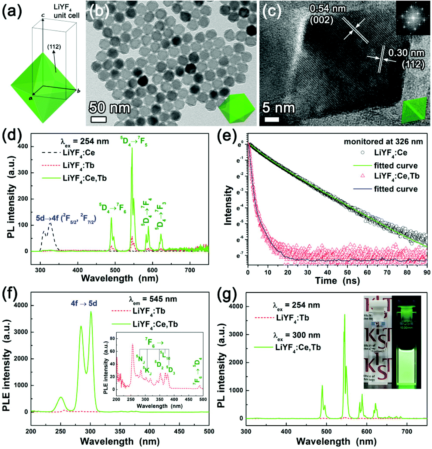 | ||
| Fig. 2 (a) Schematic illustration of a {112}-bound particle. (b) Low-magnification TEM and (c) HR-TEM images of LiYF4:Ce,Tb DCNPs. Schematic <22> and <021> views of the {112}-bound particle are inserted in (b) and (c), respectively. The inset in (c) shows a corresponding FFT pattern from the single nanophosphor. (d) PL spectra of LiYF4:Ce, LiYF4:Tb, and LiYF4:Ce,Tb under excitation with 254 nm UV light. (e) Decay profiles of LiYF4:Ce and LiYF4:Ce,Tb monitored at 326 nm for Ce3+ emission under excitation with 300 nm UV light. The green and blue solid lines are the fitted curves for the measured decay profiles of LiYF4:Ce and LiYF4:Ce,Tb, respectively. (f) PLE spectra of LiYF4:Tb and LiYF4:Ce,Tb measured at 545 nm Tb3+ emission. The inset shows the enlarged PLE spectrum of LiYF4:Tb monitored at 545 nm. (g) PL spectra of LiYF4:Tb under 254 nm excitation and LiYF4:Ce,Tb under 300 nm excitation, respectively. The inset shows the photographs of the LiYF4:Ce,Tb solution under ambient indoor light (left) and a hand-held UV lamp (λ = 300 nm) (right). | ||
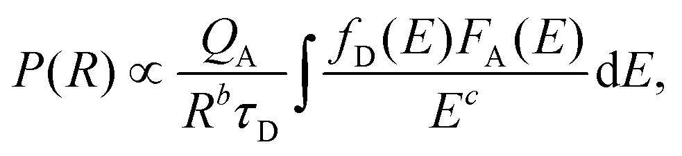
Fig. 2d–g show the measured luminescence properties of LiYF4:Ce,Tb DCNPs. In this study, PL-optimized Ce and Tb concentrations are 15 mol% (see Fig. S4 and S5†). The LiYF4:Ce,Tb DCNPs showed significantly higher PL intensity than LiYF4:Tb under excitation with 254 nm UV light. By Ce3+ sensitization, Tb3+ emission was increased by 7 times. Due to efficient energy transfer from Ce3+ to Tb3+, the Ce3+ emission peaks at about 326 nm vanished and the Tb3+ emission was considerably increased (Fig. 2d). According to Dexter,33 energy transfer from a sensitizer to an activator can be confirmed by investigating the decay time of the sensitizer. The energy transfer probability P can be expressed as follows:33
 | (1) |
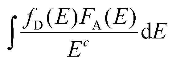 is the spectral overlap between donor emission and acceptor absorption in which fD(E) and FA(E) represent the observed shapes of the donor emission band and the acceptor absorption band, respectively. It should be noted that P is inversely proportional to τD. Fig. 2e shows the decay profiles of LiYF4:Ce and LiYF4:Ce,Tb monitored at 326 nm for Ce3+ emission. The decay profiles can be well fitted by a single second-order exponential decay function:34,35
 | (2) |
| τ* = (A1τ12 + A2τ22)/(A1τ1 + A2τ2). | (3) |
The τ* for Ce3+ was shortened from 12.3 to 0.9 ns after Tb3+ co-doping into LiYF4:Ce NCs, indicating the energy transfer from Ce3+ to Tb3+. In the PL excitation (PLE) spectrum of LiYF4:Ce,Tb measured at 545 nm for Tb3+ emission, the LiYF4:Ce,Tb DCNPs showed the maximum PLE intensity at about 300 nm (Fig. 2f and S6†). In LiYF4 with a scheelite structure, Ce3+ is located at the Y3+ sites for which the crystallographic site symmetry is S4.37,38 At this site, the Ce3+ 5d state splits into four levels and among the corresponding four absorption bands the strongest absorption is observed at approximately 300 nm.37 Thus not surprisingly, the LiYF4:Ce,Tb DCNPs emit much brighter green light under excitation with 300 nm UV light than that under excitation with 254 nm UV light (Fig. 2g). Under excitation with 300 nm UV light, LiYF4:Ce,Tb showed 65 times higher PL intensity than that of LiYF4:Tb under excitation with 254 nm UV light. Additionally, the LiYF4:Ce,Tb solution was highly transparent and colorless under ambient indoor light, whereas it showed bright green color under a hand-held UV lamp due to the intense PL peak at 545 nm ascribed to the 5D4 → 7F5 transition in Tb3+ ions (Fig. 2g inset).39
The LiYF4:Ce,Tb is now used as a DC shell for the UCNP core. Since Li(Gd,Y)F4:Yb,Er UCNPs have the same crystal structure as LiYF4,3 LiYF4:Ce,Tb can be epitaxially grown on the Li(Gd,Y)F4:Yb,Er UCNP core, resulting in Li(Gd,Y)F4:Yb,Er/LiYF4:Ce,Tb UC/DC C/S nanophosphors. An optically inert LiYF4 shell was additionally grown on the Li(Gd,Y)F4:Yb,Er/LiYF4:Ce,Tb UC/DC C/S nanophosphors to form a UC/DC/IS C/D-S architecture. The morphology and size changes during the C/D-S development were monitored step-by-step from the UC core to UC/DC C/S to UC/DC/IS C/D-S nanophosphors (Fig. 3a–c). The particle size increased by successive growth of the DC and IS shells on the core (33 ± 1 nm × 36 ± 1 nm for UC, 43 ± 2 nm × 45 ± 1 nm for UC/DC, and 51 ± 2 nm × 52 ± 1 nm for UC/DC/IS). The tetragonal bipyramidal morphologies of C/S and C/D-S NCs are also shown in the SEM images of Fig. S7 and S8.† The UC core, UC/DC, and UC/DC/IS nanophosphors have a single-crystalline tetragonal phase, judging from the XRD patterns (Fig. S9†) and HR-TEM images (Fig. S10–S12†). The formation of the DC shell was confirmed by EDX elemental analysis (Fig. 3d and e).
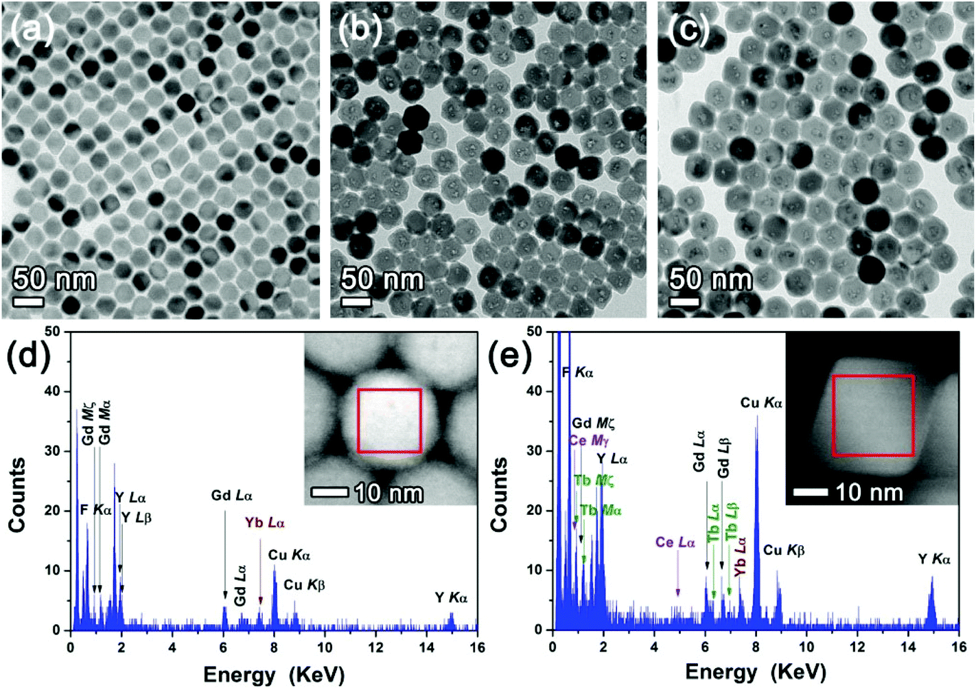 | ||
| Fig. 3 (a, b, and c) TEM images of the Li(Gd,Y)F4:Yb,Er UC core, Li(Gd,Y)F4:Yb,Er/LiYF4:Ce,Tb UC/DC C/S, and Li(Gd,Y)F4:Yb,Er/LiYF4:Ce,Tb/LiYF4 UC/DC/IS C/D-S nanophosphors, respectively. (d and e) EDX spectra of Li(Gd,Y)F4:Yb,Er UC and Li(Gd,Y)F4:Yb,Er/LiYF4:Ce,Tb UC/DC C/S nanophosphors. The STEM images of the UC core and UC/DC C/S nanophosphors with the areas where the EDX spectra were obtained are presented in the insets of (d) and (e), respectively. Only the Yb peaks were observed from a UCNP, whereas Ce and Tb (shell components) as well as Yb (core component) were detected from a UC/DC C/S nanophosphor. Note that the Er peaks were not clearly observed in the spectra, due to the weak signal-to-noise ratio with the low Er doping concentration. The Cu peaks result from the TEM grid and holder. | ||
The designed UC/DC/IS architectures were explicitly corroborated using STEM-EDX elemental line profiling and spectrum imaging. Full details of EDX analyses are provided in the ESI (Fig. S13–S15 and Table S1†). Line profilings were conducted across five primary crystallographic orientations and all experimental data were compared to the calculated profiles. Five high-symmetry line profiles are presented in Fig. 4. PF1–PF3 are considered for a nanophosphor aligned along the <110> or <021> crystallographic orientation. Since the {112}-bound tetragonal bipyramid is close to an octahedron (it is slightly elongated along the c-axis), the <110> and <021> projections are almost identical. PF4 and PF5 are considered in cases where the nanophosphor is aligned along the <22> direction which means that one of the particle faces sits on the TEM grid surface (note that this case is most commonly observed in the experiments). PF2 and PF4 have the same cross-section; but they have different thickness profiles since they sit on the TEM grid differently. This also means that slight off-orientation of the nanophosphor can induce the deviation of the line profiles from the prediction. The thickness profile was calculated using a {112}-bound C/D-S nanophosphor with the nominal compositions (Table S1†) for the core, inner shell, and outer shell as shown in Fig. 4d. The X-ray counts from Y were estimated using the thickness profile considering its composition in each region, enabling us to observe the effect of the outer shell on the Y profile even though Y is a common element in the entire particle (Fig. 4e).
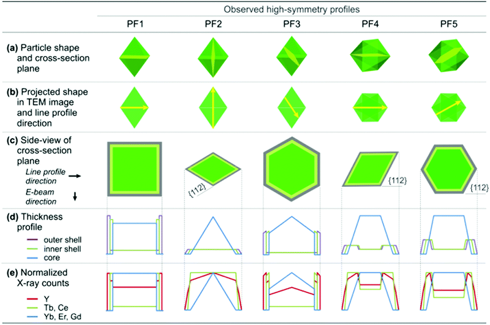 | ||
| Fig. 4 Summary of the calculated thickness profile and X-ray counts according to the nanophosphor orientations and line profile directions. (a) Particle shape and cross-section plane of the C/D-S nanophosphor, (b) projected shape in the TEM image and line profile direction, (c) side-view of the cross-section plane, (d) thickness profile, and (e) the normalized X-ray counts of each element for five primary crystallographic orientations. | ||
One representative STEM-EDX line profile data set across a C/D-S nanophosphor observed along the <22> direction is shown in Fig. 5 (see Fig. S14† for more data set). For better interpretation of the experimental result, the raw EDX line profile data were further processed to reduce the noise using a Savitzky–Golay algorithm implemented in the Origin Lab software package. Fig. 5b exhibits an example of one such processed data. It was confirmed that the processing does not produce any bias in the profile, as shown in Fig. 5b. The EDX line profile simulation (Fig. 5c) was done as depicted in Fig. 4 and compared with the experimental data (Fig. 5d). The comparison shows good agreement, indicating that Li(Gd,Y)F4:Yb,Er/LiYF4:Ce,Tb/LiYF4 C/D-S nanophosphors were successfully synthesized. The size of the core and shells was estimated to be approximately 36/5/3 nm (size of UC/thickness of DC/thickness of IS) (see Fig. S13b† for the dimensions) by comparing the experimental profiles with the simulated ones.
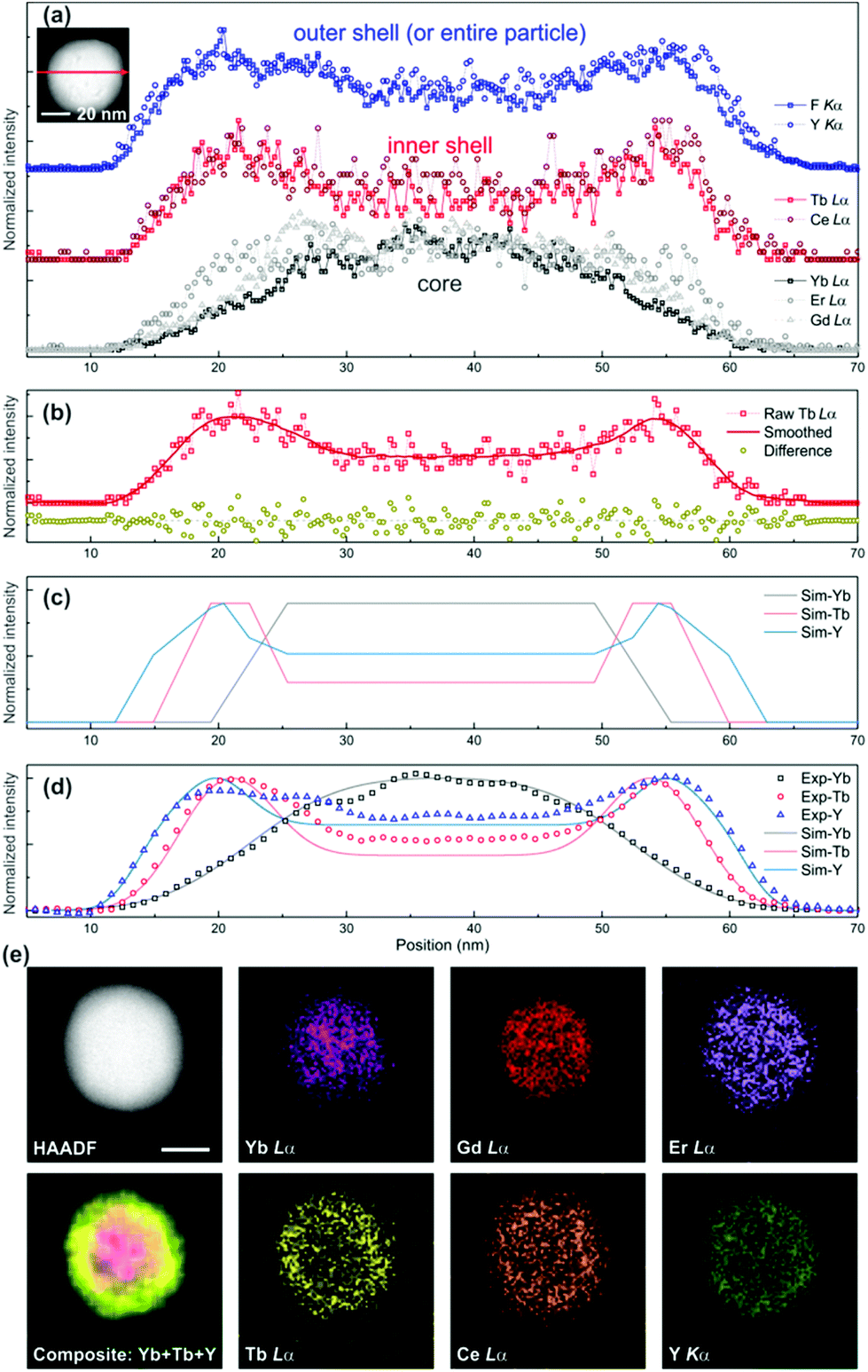 | ||
| Fig. 5 EDX line profiles across a Li(Gd,Y)F4:Yb,Er/LiYF4:Ce,Tb/LiYF4 C/D-S nanophosphor. (a) Raw line profile data for elements which are present in each region. The HAADF STEM image of the nanophosphor with the line profile direction is presented in the inset. (b) Selected raw data (Tb Lα) and its smoothed data with differences between each other. The root-mean-square deviation of the difference is 0.097 which is negligible. (c) Simulated EDX elemental profiles with a dimension of 36/5/3 nm (size of UC/thickness of DC/thickness of IS). (d) The calculated profiles (lines) were superimposed on the experimental data (open symbols), showing good agreement with the designed UC/DC/IS architecture. The simulated profiles were Gaussian-broadened which could occur by experimental uncertainty (see the ESI†). (e) EDX maps of Yb Lα, Gd Lα, Er Lα, Tb Lα, Ce Lα, and Y Kα from a Li(Gd,Y)F4:Yb,Er/LiYF4:Ce,Tb/LiYF4 C/D-S nanophosphor. The composite STEM-EDX map of the nanophosphor was produced by superposing the Yb Lα (magenta), Tb Lα (yellow), and Y Kα (green) maps. The EDX maps are presented by the X-ray counts acquired from each X-ray peak such that all maps span the maximum and minimum intensities of each image. No image processing was performed on individual maps, while the composite map was noise-filtered. The size difference between core elements (Yb, Gd, and Er) and inner shell elements (Tb and Ce) is clearly seen. The scale bar is 20 nm in length. | ||
The C/D-S structures were further visualized by EDX spectrum imaging (Fig. 5e and S15†). The EDX maps from the core elements (Yb, Gd, and Er) appear to be clearly confined in the UC core region while the ones from the shell elements span the particle with stronger signals in the DC shell region. The size difference between the EDX maps from Tb (or Ce) and Y is small but detectable as shown in the line profile. In addition to the size difference between the core and shell elemental maps, it should be noted that there is another noteworthy difference between the EDX maps from Yb/Gd and Er; Yb and Gd tend to be located more in the central region of the UC core while Er distributes over a larger area in the core. The shell elements also show slightly different distributions in the shell (Fig. 5e and S15†). Currently, the distribution and location preference of each element in the nanophosphor are under study.
The PL properties of the UC core, UC/DC C/S, and UC/DC/IS C/D-S nanophosphors under excitations with 980 nm NIR and 300 nm UV lights were investigated (Fig. 6a and b). Fig. 6a shows the PL enhancement of the UCNPs by the formation of UC/DC and UC/DC/IS architectures under excitation with 980 nm NIR light. The UCL intensity of Li(Gd,Y)F4:Yb,Er at 552 nm, the peak wavelength, was enhanced by 335% after the formation of the LiYF4:Ce,Tb DC shell and further enhanced by 340% compared with the UC core via growth of the LiYF4 IS layer on the UC/DC C/S. The effect of LiYF4 coating on the UC/DC C/S was remarkable for DCL under excitation with 300 nm UV light. The Li(Gd,Y)F4:Yb,Er showed no luminescence under excitation with 300 nm UV light, whereas the UC/DC C/S nanophosphors exhibited strong green luminescence under the same excitation conditions, as shown in Fig. 6b and c. The DCL from the LiYF4:Ce,Tb shell was further enhanced by LiYF4 coating. The PL intensity of the LiYF4:Ce,Tb was increased by 2.2 times after LiYF4 coating. In addition to the PL spectra, the photographs simultaneously displaying both UCL and DCL from the UC/DC and UC/DC/IS nanophosphor solutions under excitations with NIR and UV light, directly show that our designed UC/DC/IS nanophosphors exhibit intense dual-mode luminescence.
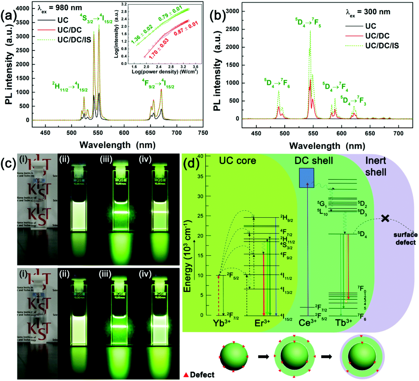 | ||
| Fig. 6 PL spectra of Li(Gd,Y)F4:Yb,Er UC, Li(Gd,Y)F4:Yb,Er/LiYF4:Ce,Tb UC/DC, and Li(Gd,Y)F4:Yb,Er/LiYF4:Ce,Tb/LiYF4 UC/DC/IS nanophosphors under excitations with (a) 980 nm NIR and (b) 300 nm UV lights. (c) Photographs of the UC/DC nanophosphor solution (upper panel) and the UC/DC/IS nanophosphor solution (lower panel) under (i) ambient room light, (ii) hand-held UV lamp illumination (λ = 300 nm), (iii) 980 nm NIR laser, and (iv) combined UV and NIR illumination. The photographs were taken with exposure times of 0.025 s. (d) Schematic energy level diagram showing UC and DC emissions from the UC/DC/IS C/D-S nanophosphors (upper panel). The lower panel shows how the shell formation suppresses the surface defects. The surface defects of the core nanoparticle may be partially retained. The inset shows the UC PL intensities of green and red emission peaks of C/D-S nanophosphors as a function of incident laser power density. | ||
As depicted in Fig. 6d, the defects of the Li(Gd,Y)F4:Yb,Er UC core such as surface traps caused by the dangling bonds can be significantly reduced by formation of a LiYF4:Ce,Tb DC shell. As a result, UCL via electronic transitions from the 2H11/2, 4S3/2, and 4F9/2 levels to the 4I15/2 level can be considerably enhanced (Fig. 6a). However, the contribution of the inert LiYF4 shell to UCL enhancement was limited because the LiYF4:Ce,Tb DC shell obstructed the interaction between dopant Er3+ ions and surface oscillators, which typically occurs within a distance of ∼3 nm.22,40 As observed in colloidal LiYF4:Ce,Tb DCNPs, the Li(Gd,Y)F4:Yb,Er/LiYF4:Ce,Tb UC/DC C/S nanophosphors showed strong characteristic Tb3+ emission peaks via5D4 → 7FJ (J = 0, 1, 2, 3, 4, 5, and 6) transitions under excitation with 300 nm UV light. Similar to the enhancement of Er3+ luminescence by the formation of a DC shell, Tb3+ luminescence was largely enhanced by the formation of a LiYF4 shell on the UC/DC nanophosphors due to the surface passivation effects (including the decreased density of the surface defects and the obstruction of the interaction between Tb3+ dopants and surface oscillators).17 Consequently, the UC/DC/IS C/D-S nanophosphors exhibit strong UCL from the UC core and intense DCL from the DC shell due to decreased surface quenching, when they are excited with 980 nm NIR and 300 nm UV lights (Fig. 6d). The absolute QEs of UCL and DCL can be obtained by the ratio of the number of emitted photons and the number of absorbed photons.41,42 The absolute UC QE of the C/D-S NPs was measured by using an integrating sphere at several laser powers because UC QE depends on the incident laser power density due to the non-linear properties of the UC process.43 The UC QE of the C/D-S NPs was measured to be 3.8% at 239 W cm−2 (see the ESI† for detail, Fig. S16, 17 and Table S2†). The absolute DC QE of the C/D-S NPs was also measured by using an integrating sphere and the value was 73.0 ± 0.1%. In addition, we recorded the UC PL spectra of the C/D-S NPs under various incident laser powers to investigate the saturation effect (Fig. S18†). The UC PL intensities of green and red emission peaks of C/D-S NPs versus the laser power density are plotted on a double-logarithmic scale and the double-logarithmic plots were fitted linearly (Fig. 6a inset). The fitted slopes are 1.36 ± 0.02 and 1.70 ± 0.03 for green and red emissions, respectively at a low power density region (<∼663 W cm−2). On the other hand, the slope decreased to 0.79 ± 0.01 and 0.87 ± 0.01 for green and red emissions, respectively at a high power density region, suggesting that the saturation effect occurs at a laser power density higher than ∼663 W cm−2.
Since Er3+ and Tb3+ co-activated LiYF4-based C/S nanophosphors can create dual-mode luminescence and surface quenching can also be suppressed from the LiYF4 shell in the C/S nanophosphors, it is worth comparing our C/D-S nanophosphors with LiYF4:Ce,Tb,Yb,Er/LiYF4 C/S nanophosphors. It was found that when the LiYF4 NCs were co-doped with both DC and UC activators, they showed weak UC emission (even weaker than the Li(Gd,Y)F4:Yb,Er core UCNPs) as shown in Fig. S19.† This result is probably due to dissipation of the excitation energy through energy transfer from Yb3+ and Er3+ to the 7FJ manifolds of Tb3+ (Fig. S20†).6 In addition, the shorter PL decay time for Er3+ emission in LiYF4:Ce,Tb,Yb,Er/LiYF4 than that in Li(Gd,Y)F4:Yb,Er supports the energy transfer from Er3+ to Tb3+ (Fig. S21†). They also showed weak DCL because the deleterious cross-relaxation between Er3+ and Tb3+ was predominant due to the high dopant concentration, making Er3+ and Tb3+ closer (Fig. S20†).15 The shorter Tb3+ decay time also supports the energy transfer from Tb3+ to Er3+ as shown in Fig. S22.†
To examine the effect of the particle size on the brightness of dual-mode luminescence, we synthesized much smaller UC/DC/IS C/D-S nanophosphors via the use of the ultrasmall UC cores synthesized by controlling the Y concentration in Li(Gd,Y)F4:Yb,Er.3 When sub-10 nm LiYF4:Yb,Er was used as a UC core, ∼15 nm LiYF4:Yb,Er/LiYF4:Ce,Tb/LiYF4 UC/DC/IS nanophosphors were synthesized with no impurity phases (Fig. S23†). When the UC core size decreased from ∼36 (more precisely 33 ± 1 nm × 36 ± 1 nm) to ∼9 nm (9 ± 1 nm), the UCL intensity was significantly decreased due to extremely increased surface defects per unit volume, as shown in Fig. S24.†17 Due to the weak UCL intensity of the ultrasmall UC cores, the UCL intensities of the small C/S (12 ± 1 nm) and C/D-S (15 ± 1 nm) NCs are much lower than those of the large C/S and C/D-S NCs (Fig. S25a†). However, the UCL enhancement factors (EFs) for the small C/S and C/D-S NCs were calculated to be 6.50 and 16.50 while the UCL EFs for the large C/S and C/D-S NCs were calculated to be 3.23 and 3.26 (Fig. S25b†). These results indicate that the formation of inner DC and outer IS layers on the small UC cores is more effective to the UCL enhancement compared with the large UC core-based C/S and C/D-S NCs and the outer inert shell contribution to UCL enhancement depends on the size of the UC core. Although the PL intensity of the small C/D-S NCs (15 ± 1 nm) is lower than that of the large C/D-S NCs (51 ± 2 nm × 52 ± 1 nm), the small C/D-S NCs still exhibit relatively bright dual-mode green luminescence under the excitations with UV and NIR lights as shown in the photographs of Fig. S26.†
The feasibility of the Li(Gd,Y)F4:Yb,Er/LiYF4:Ce,Tb/LiYF4 C/D-S nanophosphors to be used for transparent display devices was investigated by incorporating the UC/DC/IS nanophosphors into a PDMS polymer. As shown in Fig. 7a, a highly transparent UC/DC/IS nanophosphor–PDMS composite bar and a disk were successfully prepared. The uniform green light emission from the nanophosphor–PDMS composites under both NIR laser irradiation and hand-held UV lamp illumination indicates that the UC/DC/IS nanophosphors were homogeneously dispersed in the PDMS polymer (Fig. 7b and c). Like the UC/DC/IS nanophosphors in solvent, the nanophosphor–PDMS composites emitted bright dual-mode green light under illumination with NIR and UV lights, as shown in Fig. 7d.
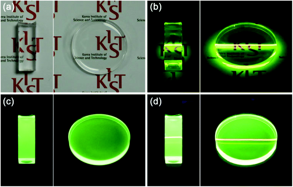 | ||
| Fig. 7 Photographs of the UC/DC/IS C/D-S nanophosphor-PDMS polymer bar (left) and disk (right) under (a) ambient indoor light, (b) 980 nm NIR laser, (c) hand-held UV lamp (λ = 300 nm), and (d) simultaneous illumination with an NIR laser and a hand-held UV lamp. The photographs were taken with exposure times of 0.01 s for (a) and 0.025 s for (b)–(d) with other conditions fixed. | ||
4. Conclusions
In summary, intense DC green-emitting LiYF4:Ce,Tb nanophosphors and bright dual-mode green-emitting Li(Gd,Y)F4:Yb,Er/LiYF4:Ce,Tb/LiYF4 C/D-S nanophosphors with tetragonal bipyramidal morphologies have been synthesized for the first time. Separation of UC- and DC-emitting activators with appropriate sensitizer ions into the UC core and DC shell, and outer inert shell layer led to bright dual-mode luminescence from a single nanophosphor. The C/D-S architecture of tetragonal bipyramidal nanophosphors has been verified by low-voltage STEM-EDX analyses with the assistance of line profile simulation. These C/D-S nanophosphors were successfully incorporated into the PDMS polymer and the C/D-S nanophosphor–PDMS composites also showed bright dual-mode green light. Due to the bright dual-mode luminescence properties of the UC/DC/IS C/D-S nanophosphors, the nanophosphors show promising applications as multiplexed luminescent imaging agents and emitters in three-dimensional volumetric displays.Acknowledgements
This work was supported by the Future Key Technology Program (2E25371) by the Korea Institute of Science and Technology (KIST), the Pioneer Research Center Program through the National Research Foundation of Korea funded by the Ministry of Science, ICT & Future Planning (NRF-2013M3C1A3065040), and the MRSEC Program of the National Science Foundation (NSF) under Award number DMR-1420013. Parts of this work were carried out in the Characterization Facility, University of Minnesota, which receives equipment funding through the UMN NSF MRSEC. We thank Michael Odlyzko for critically reading the manuscript.References
- G. Chen, H. Qiu, P. N. Prasad and X. Chen, Chem. Rev., 2014, 114, 5161 CrossRef CAS PubMed.
- S. Gai, C. Li, P. Yang and J. Lin, Chem. Rev., 2013, 114, 2343 CrossRef PubMed.
- H. Na, J. S. Jeong, H. J. Chang, H. Y. Kim, K. Woo, K. Lim, K. A. Mkhoyan and H. S. Jang, Nanoscale, 2014, 6, 7461 RSC.
- H. Na, K. Woo, K. Lim and H. S. Jang, Nanoscale, 2013, 5, 4242 RSC.
- S. Y. Kim, K. Woo, K. Lim, K. Lee and H. S. Jang, Nanoscale, 2013, 5, 9255 RSC.
- F. Wang, Y. Han, C. S. Lim, Y. Lu, J. Wang, J. Xu, H. Chen, C. Zhang, M. Hong and X. Liu, Nature, 2010, 463, 1061 CrossRef CAS PubMed.
- Z. L. Wang, Z. W. Quan, P. Y. Jia, C. K. Lin, Y. Luo, Y. Chen, J. Fang, W. Zhou, C. J. O′Connor and J. Lin, Chem. Mater., 2006, 18, 2030 CrossRef CAS.
- Y. Dai, H. Xiao, J. Liu, Q. Yuan, P. Ma, D. Yang, C. Li, Z. Cheng, Z. Hou, P. Yang and J. Lin, J. Am. Chem. Soc., 2013, 135, 18920 CrossRef CAS PubMed.
- S. Wu, G. Han, D. J. Milliron, S. Aloni, V. Altoe, D. V. Talapin, B. E. Cohen and P. J. Schuck, Proc. Natl. Acad. Sci. U. S. A., 2009, 106, 10917 CrossRef CAS PubMed.
- Y. I. Park, J. H. Kim, K. T. Lee, K.-S. Jeon, H. B. Na, J. H. Yu, H. M. Kim, N. Lee, S. H. Choi, S.-I. Baik, H. Kim, S. P. Park, B.-J. Park, Y. W. Kim, S. H. Lee, S.-Y. Yoon, I. C. Song, W. K. Moon, Y. D. Suh and T. Hyeon, Adv. Mater., 2009, 21, 4467 CrossRef CAS.
- K. Kömpe, H. Borchert, J. Storz, A. Lobo, S. Adam, T. Möller and M. Haase, Angew. Chem., Int. Ed., 2003, 42, 5513 CrossRef PubMed.
- C. Li and J. Lin, J. Mater. Chem., 2010, 20, 6831 RSC.
- J.-C. Boyer, J. Gagnon, L. A. Cuccia and J. A. Capobianco, Chem. Mater., 2007, 19, 3358 CrossRef CAS.
- P. Li, Q. Peng and Y. D. Li, Adv. Mater., 2009, 21, 1945 CrossRef CAS.
- Y. Liu, D. Tu, H. Zhu, R. Li, W. Luo and X. Chen, Adv. Mater., 2010, 22, 3266 CrossRef CAS PubMed.
- G. Blasse and B. C. Grabmaier, Luminescent Materials, Springer, Berlin, 1994 Search PubMed.
- F. Wang, J. Wang and X. Liu, Angew. Chem., Int. Ed., 2010, 49, 7456 CrossRef CAS PubMed.
- H. S. Jang, K. Woo and K. Lim, Opt. Express, 2012, 20, 17107 CrossRef CAS.
- J.-C. Boyer, M.-P. Manseau, J. I. Murray and F. C. J. M. van Veggel, Langmuir, 2009, 26, 1157 CrossRef PubMed.
- H. S. Kiliaan, A. Meijerink and G. Blasse, J. Lumin., 1986, 35, 155 CrossRef CAS.
- S. Y. Kim, Y.-H. Won and H. S. Jang, Sci. Rep., 2015, 5, 7866 CrossRef CAS PubMed.
- Q. Su, S. Han, X. Xie, H. Zhu, H. Chen, C.-K. Chen, R.-S. Liu, X. Chen, F. Wang and X. Liu, J. Am. Chem. Soc., 2012, 134, 20849 CrossRef CAS PubMed.
- F. Wang, R. Deng, J. Wang, Q. Wang, Y. Han, H. Zhu, X. Chen and X. Liu, Nat. Mater., 2011, 10, 968 CrossRef CAS PubMed.
- K. A. Abel, J.-C. Boyer and F. C. J. M. van Veggel, J. Am. Chem. Soc., 2009, 131, 14644 CrossRef CAS PubMed.
- K. A. Abel, J.-C. Boyer, C. M. Andrei and F. C. J. M. van Veggel, J. Phys. Chem. Lett., 2011, 2, 185 CrossRef CAS.
- F. Zhang, R. Che, X. Li, C. Yao, J. Yang, D. Shen, P. Hu, W. Li and D. Zhao, Nano Lett., 2012, 12, 2852 CrossRef CAS PubMed.
- X. Li, R. Wang, F. Zhang and D. Zhao, Nano Lett., 2014, 14, 3634 CrossRef CAS PubMed.
- H. Wen, H. Zhu, X. Chen, T. F. Hung, B. Wang, G. Zhu, S. F. Yu and F. Wang, Angew. Chem., Int. Ed., 2013, 52, 13419 CrossRef CAS PubMed.
- L. Zhang, Z. Wang, Z. Lu, K. Xia, Y. Deng, S. Li, C. Zhang, Y. Huang and N. He, J. Nanosci. Nanotechnol., 2014, 14, 4710 CrossRef CAS PubMed.
- V. Mahalingam, F. Vetrone, R. Naccache, A. Speghini and J. A. Capobianco, Adv. Mater., 2009, 21, 4025 CrossRef CAS.
- J. Park, K. An, Y. Hwang, J.-G. Park, H.-J. Noh, J.-Y. Kim, J.-H. Park, N.-M. Hwang and T. Hyeon, Nat. Mater., 2004, 3, 891 CrossRef CAS PubMed.
- H. S. von Harrach, P. Dona, B. Freitag, H. Soltau, A. Niculae and M. Rohde, J. Phys.: Conf. Ser., 2010, 241, 012015 CrossRef.
- D. L. Dexter, J. Chem. Phys., 1953, 21, 836 CrossRef CAS.
- M. Yu, J. Lin and J. Fang, Chem. Mater., 2005, 17, 1783 CrossRef CAS.
- S. Kim, T. Kim, M. Kang, S. K. Kwak, T. W. Yoo, L. S. Park, I. Yang, S. Hwang, J. E. Lee, S. K. Kim and S.-W. Kim, J. Am. Chem. Soc., 2012, 134, 3804 CrossRef CAS PubMed.
- T. Moon, G. Y. Hong, H.-C. Lee, E.-A. Moon, B. W. Jeoung, S.-T. Hwang, J. S. Kim and B.-G. Ryu, Electrochem. Solid-State Lett., 2009, 12, J61 CrossRef CAS.
- C. M. Combes, P. Dorenbos, C. W. E. van Eijk, C. Pedrini, H. W. Den Hartog, J. Y. Gesland and P. A. Rodnyi, J. Lumin., 1997, 71, 65 CrossRef CAS.
- D. J. Ehrlich, P. F. Moulton and R. M. Osgood, Jr., Opt. Lett., 1979, 4, 184 CrossRef CAS PubMed.
- Y.-C. Li, Y.-H. Chang, Y.-F. Lin, Y.-S. Chang and Y.-J. Lin, Electrochem. Solid-State Lett., 2006, 9, H74 CrossRef CAS.
- L. P. Qian, D. Yuan, G. S. Yi and G. M. Chow, J. Mater. Res., 2009, 24, 3559 CrossRef CAS.
- J.-C. Boyer and F. C. J. M. van Veggel, Nanoscale, 2010, 2, 1417 RSC.
- S. H. Park, A. Hong, J.-H. Kim, H. Yang, K. Lee and H. S. Jang, ACS Appl. Mater. Interfaces, 2015, 7, 6764 CAS.
- F. Auzel, Chem. Rev., 2004, 104, 139 CrossRef CAS PubMed.
Footnotes |
| † Electronic supplementary information (ESI) available: XRD patterns, PL and PLE spectra, SEM and HR-TEM images, PL decay times, photographs showing the transparent nanophosphor solutions and their dual-mode luminescence, and additional EDX data. See DOI: 10.1039/c5nr05722a |
| ‡ These authors contributed equally to this work. |
| This journal is © The Royal Society of Chemistry 2016 |