
Silicon oxide nanowire growth mechanisms revealed by real-time electron microscopy†
Miroslav
Kolíbal
*ab,
Libor
Novák
c,
Toby
Shanley
d,
Milos
Toth
d and
Tomáš
Šikola
ab
aInstitute of Physical Engineering, Brno University of Technology, Technická 2, 616 69 Brno, Czech Republic
bCEITEC BUT, Brno University of Technology, Technická 10, 61669 Brno, Czech Republic
cFEI Company, Vlastimila Pecha 1282/12, 627 00 Brno, Czech Republic. E-mail: kolibal.m@fme.vutbr.cz
dSchool of Mathematical and Physical Sciences, University of Technology, Sydney, Ultimo 2007, Australia
First published on 26th November 2015
Abstract
Growth of one-dimensional materials is possible through numerous mechanisms that affect the nanowire structure and morphology. Here, we explain why a wide range of morphologies is observed when silicon oxide nanowires are grown on silicon substrates using liquid gallium catalyst droplets. We show that a gallium oxide overlayer is needed for nanowire nucleation at typical growth temperatures, and that it can decompose during growth and, hence, dramatically alter the nanowire morphology. Gallium oxide decomposition is attributed to etching caused by hydrogen that can be supplied by thermal dissociation of H2O (a common impurity). We show that H2O dissociation is catalyzed by silicon substrates at temperatures as low as 320 °C, identify the material supply pathways and processes that rate-limit nanowire growth under dry and wet atmospheres, and present a detailed growth model that explains contradictory results reported in prior studies. We also show that under wet atmospheres the Ga droplets can be mobile and promote nanowire growth as they traverse the silicon substrate.
1. Introduction
Nanowires (NWs) and nanorods are an attractive class of nanostructured materials because they possess improved and new functionalities over their bulk counterparts. One-dimensional nanostructures have large surface-to-volume ratios that are beneficial for sensing, and a geometry that represents a promising new building block for devices.1–4 Oxide nanowires possess many remarkable properties, and a large amount of knowledge is available on the functionality, chemistry and chemical modification of silica surfaces which can be used as active surfaces of sensors modified by various receptors, or biologically active composites that mimic enzyme activities.5 The affinity of silica for biomolecules is increased further if substoichiometric oxide compositions (SiOx, where x < 2) are realized.6 Silicon oxide nanowires thus represent an ideal building block for photoactive,7 sensing8 and biosensing9–11 devices with improved sensitivity over the current state-of-the-art systems.12,13Fabrication of nanowire-based devices requires a detailed understanding of NW growth mechanisms. The most investigated mechanism uses catalytic metal seeds to induce one-dimensional growth, and each specific process is denoted by the material pathway that leads to growth. For example, in vapor–liquid–solid growth (VLS) metallic droplets catalyze the decomposition of gaseous precursor molecules or act as collectors of diffusing adatoms. Nucleation is preferred at the solid/liquid interface between the droplet and the substrate14 and nanowires grow with the droplet on top. However, due to thermodynamic limitations (the Gibbs–Thompson effect)15 the growth of NWs with very small diameters (<10 nm) is extremely challenging. In solid–liquid–solid (SLS)16,17 growth, the substrate material is dissolved in liquid droplets and precipitates on the droplet surfaces. It is common for multiple nanowires with small diameters (<20 nm) and extreme length (several millimeters)18 to grow on top of each collector droplet.19 Hence, SLS growth is a promising process for circumventing the Gibbs–Thompson effect.
Low-melting point metal catalysts are advantageous because they reduce nanowire growth temperatures. However, these materials oxidize under ambient conditions, which can alter or inhibit growth. Nevertheless, Sunkara et al. demonstrated the growth of silicon nanowires from the molten Ga catalyst20 and soon thereafter Pan et al.21 and Zheng et al.18 reported silicon oxide nanowires grown from Ga annealed at a high temperature in an oxidative environment. The technique was subsequently utilized by other groups22–26 using various low-melting-point catalysts.27–32 Numerous nanowire morphologies have been demonstrated33,34 such as dense bunches of nanowires that grow from the catalyst particle,18,21,26,33–35 and nanowire shells around the catalyst particles.22,23 The particles are either pinned to the surface22–24 or elevated above it.25,26,33,34 The wide variety of observed morphologies is indicative of a complex growth mechanism. It is unclear whether the growth species diffuse through the droplet36 or across the droplet surface,24,37 or if supersaturation is reached in the gas phase or the liquid phase. The most compelling model of growth is based on the attachment of the growth species to nanowire roots that is preferred over the formation of new nuclei,14,37 although other models have been proposed.38
Here, we use several experiments to elucidate the nanowire growth mechanism in the SiOx (nanowire)–Ga (droplet)–Si(substrate) system. We show that the presence of water or hydrogen has a critical effect on the morphology of the growth products that we attribute to etching of a thin gallium oxide overlayer that typically forms on the catalyst particles during sample preparation. In the absence of water (or hydrogen), silicon oxide nanowires nucleate below the gallium oxide shell and grow towards the gallium core. However, when water (or hydrogen) is present in the system, the oxide shell is removed and nanowire bunches grow from the surface of each gallium droplet. Our experiments indicate that the oxide shell is necessary for nucleation and that the growth interface is located at the surface of the liquid metal catalyst, thus supporting the hypothesis that one-dimensional growth is driven by surface energy minimization during growth. Real-time electron imaging reveals the processes that rate-limit growth and provides direct evidence for the extreme mobility of Ga catalyst particles. Our results can likely explain the wide range of NW morphologies reported in the literature.
2. Experimental section
2.1 Sample preparation and nanowire growth
Nanowires were grown in two separate instruments. Most experiments were performed in an environmental reaction cell located inside a scanning electron microscope (SEM). The cell houses a gas cascade electron detector, a high temperature sample heater, capacitance manometer and is connected to a gas delivery system regulated by a mass-flow controller. The electron microscope chamber is pumped down to high vacuum (base pressure of 5 × 10⁻⁴ Pa) while SEM imaging is performed inside the reaction cell at gas pressures of up to 4 kPa. To prepare large Ga catalyst droplets, molten Ga was spread onto a piece of a Si wafer (both (111) and (100) orientations were used, with similar results), previously etched in buffered HF to remove the native silicon oxide. Samples were immediately loaded into the reaction chamber, pumped down to high vacuum, heated up to the desired growth temperature (200–930 °C) and the oxidizing gas was introduced (oxygen – purity 99.999%, nitrogen – purity 99.9%, or water vapor).Gallium droplets and silicon oxide nanowires were also fabricated using an ultra-high vacuum (UHV, base pressure <8 × 10⁻⁸ Pa) cluster tool that allows in situ Ga evaporation, exposure to controlled gaseous atmospheres (maximum pressure of 5 × 10⁻² Pa) and analysis by X-ray photoelectron spectroscopy (XPS). Small Ga droplets (below 500 nm) were evaporated onto Si substrates under UHV conditions at different substrate temperatures (150–300 °C) to produce ensembles of Ga droplets with an uniform size.39 The samples were either used for growth immediately or subsequently exposed to the ambient atmosphere to enable gallium oxide shell formation. After oxidation, the samples were used for growth in a SEM reaction chamber or reinserted into the UHV chamber.
2.2 XPS analysis of gallium oxide decomposition
XPS spectra of the clean samples were taken using Al Kα radiation (1486.6 eV) at an electron exit angle of 41° with respect to the surface plane. After XPS measurements, the sample was transferred under UHV conditions to another UHV chamber and exposed for 10 minutes to pure oxygen (99.999%) or water vapor at an elevated temperature. The maximum allowable pressure in the chamber is 6 × 10⁻² Pa, which is significantly lower than the pressure during nanowire growth inside the SEM reaction chamber. Hence, to check for the relevance of these experiments, we have checked ex situ that the nanowire growth proceeds also at these low pressures. Note that the XPS measurements were performed after sample cooling from the reaction temperature. To avoid compromising the results by post-oxidation or thermal decomposition of the oxide, we performed sample cooling under both high vacuum and oxidizing atmospheres with similar results.2.3 Real time energy dispersive X-ray spectroscopy measurements
Real time energy dispersive X-ray spectroscopy measurements were performed in a similar microscope as the growth experiments, equipped with an EDX detector and a hot stage. Samples were prepared as for NW growth by spreading liquid Ga onto a buffered-HF etched Si substrate. They were annealed at 550 °C under high vacuum (5 × 10⁻³ Pa). The X-ray signal was excited using a 5 keV electron beam focused onto a large gallium droplet (10 μm in diameter) and detected in a 200 eV-energy window centered on 1.74 keV (Si Kα). The Monte Carlo code CASINO40 was used to simulate the maximum X-ray generation depth in Ga, which is smaller than 200 nm at 5 keV. Hence, the X-ray signal was generated exclusively in the near-surface region of the catalyst droplet.The growth products were also analyzed ex situ by high resolution SEM, microscopic Fourier Transform Infrared Spectroscopy (FTIR) and cathodoluminescence spectroscopy.
3. Results and discussion
We analyzed the growth products by ex situ, high resolution SEM. Representative images of structures grown for 10 minutes under dry and wet atmospheres (at 930 and 500 °C, respectively) are shown in Fig. 1. If a dry oxidative agent is used (nitrogen containing oxygen traces, Fig. 1a–c), the large Ga droplets are encapsulated by a thick porous shell. Closer inspection of the shell morphology is possible because it is usually cracked, revealing that the shell is made of nanowires (Fig. 1b). NW shells were observed to encapsulate Ga droplets with diameters ranging from several hundred nanometers to a millimeter, which is consistent with prior reports.21–23,28,31 Chemical analysis confirms that the nanowires consist of non-stoichiometric silicon oxide (see ESI S1† for details). A variety of structures was found after growth – catalyst droplets with a single nanowire shell (Fig. 1a), droplets with multiple, onion-like nanowire shells and complex, exotic, faceted multilayers (see ESI S2†). Additional examples can be found in the literature.21,29,30,33 Every Ga droplet with a nanowire shell has an etch pit at the base (see Fig. 1c and ESI S2†), indicating that the substrate material was consumed during growth.18,22,23,30 High resolution electron microscopy images show the presence of a very thin compact layer at the outer part of the shell (Fig. 1b and c). The presence of such a layer was also reported previously, and chemical analysis showed that it is composed mainly of Ga and O atoms.21 We have examined this layer in more detail by site-selective cathodoluminescence measurements (see ESI S3†), showing that it is native Ga2O3 and below we will show that it plays a crucial role in promoting nanowire growth.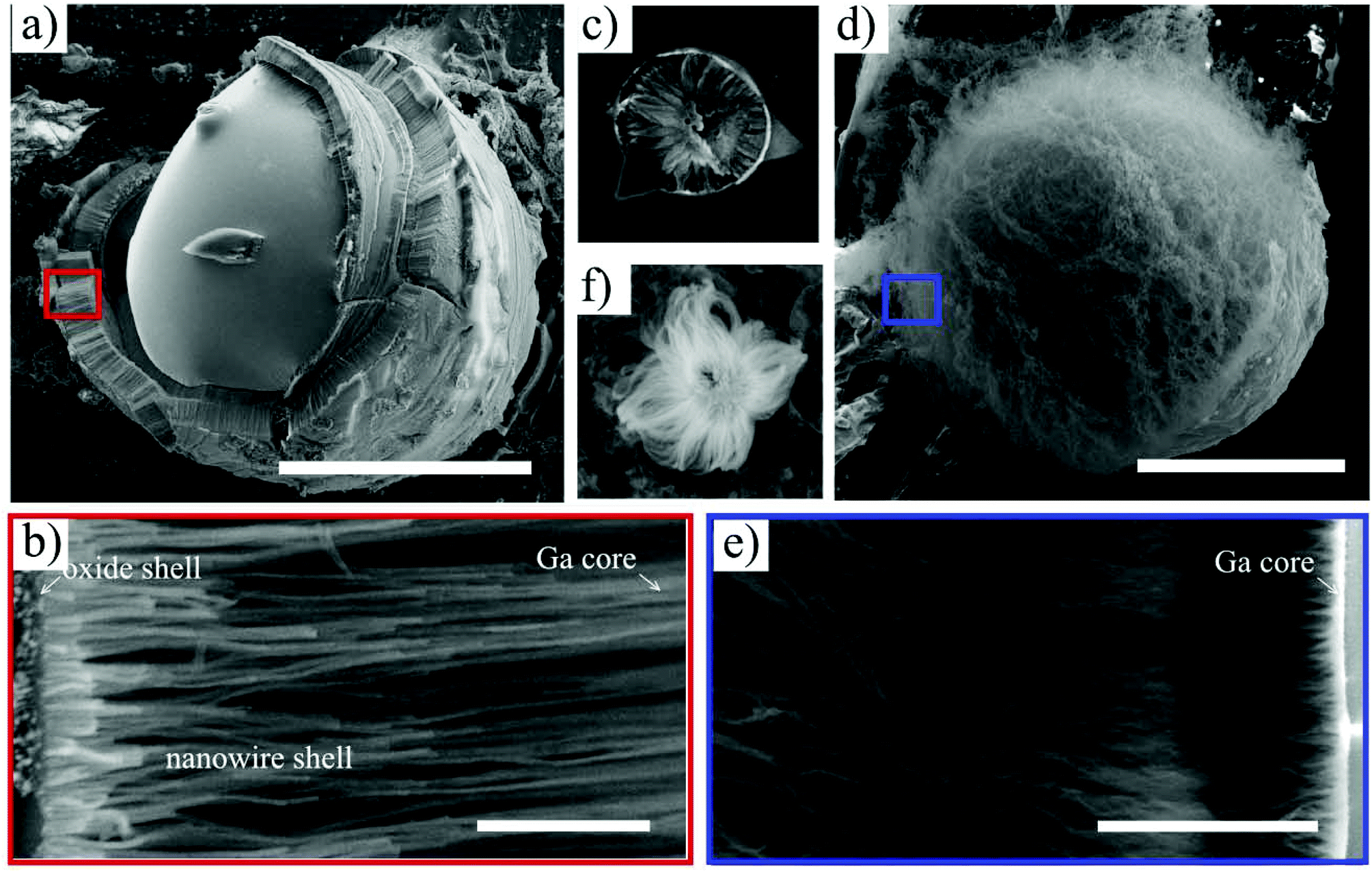 | ||
| Fig. 1 (a–c) Ex situ SEM images of growth products fabricated under a dry oxidizing atmosphere at 600 Pa nitrogen and 930 °C. (a) A large Ga droplet, exhibiting a thick shell made of silicon oxide nanowires; scale bar, 50 μm. (b) Magnified image of the nanowire shell marked by a red rectangle in (a); scale bar, 500 nm. (c) Silicon oxide nanowires grown from a small catalyst droplet. Here, the Ga catalyst had an initial diameter of 300 nm. After growth, the Ga core is completely expelled from the droplet, and the remaining product consists of nanowires encapsulated by a gallium oxide shell. A triangular etch pit is clearly visible below the droplet. (d–f) Ex situ SEM images of growth products fabricated under a wet oxidizing atmosphere at 250 Pa of water vapor and 500 °C. (d) A large Ga droplet, surrounded by dense bunches of silicon oxide nanowires; scale bar, 5 μm, (e) Magnified image of the silicon oxide nanowires marked by a blue rectangle in (d); scale bar, 500 nm, (f) Nanowire bunches grown from a small Ga droplet (300 nm in diameter). | ||
A very distinct nanowire morphology is observed if water vapor is introduced into the growth chamber. Unlike the highly-aligned nanowires grown in a dry oxidizing gas, water-oxidized NWs grow in bunches outwards from the surface of the catalyst droplet (Fig. 1d–f), and individual nanowires have a stranded morphology. This is observed even if very small (<300 nm) Ga droplets are used to catalyze the growth (Fig. 1f). The etch pits below the catalyzing droplets are present, as in the case of a dry oxidizing gas (see ESI S4†). Notably, if the oxidizing atmosphere is not precisely controlled, both nanowire morphologies can be observed (see ESI S2†). In this experiment, a small leak to the gas delivery system was introduced and, therefore, the nitrogen atmosphere (300 Pa) contained a small amount of water vapor.
The parameter window for nanowire growth is wide and similar for both dry and wet oxidation. Nanowires were successfully fabricated at temperatures in the range of 200 to 930 °C (higher temperatures were not tested). Growth took place at pressures as high as 4 kPa (in the SEM reaction cell), and as low as 10−2 Pa (in the UHV chamber). The nanowire diameter (7–20 nm) is only slightly dependent on temperature, as predicted by theoretical models.26,41 The nanowires grown in water vapor exhibit consistently smaller diameters than those grown under a dry atmosphere. The growth experiments in the UHV chamber, where the gallium catalyst can be evaporated in situ without exposure to ambient conditions (and so does not contain a native oxide), have resulted in the important conclusion that the gallium oxide is necessary for nanowire growth. Without the oxide shell, NW growth was not observed under a wet atmosphere and only occasionally under a dry atmosphere (where the re-oxidation of the catalyst can eventually take place).
3.1 NW growth under a dry atmosphere
The ex situ inspection of the dry-oxidation growth products (Fig. 1b) shows that the nanowires grow between the native oxide shell and the gallium core. To elucidate the growth mechanism, we start by analyzing mass transport of the reactants to the growth interface. To unravel the silicon supply pathway, we measured the elemental composition of a catalyst droplet during annealing under high vacuum by in situ Energy Dispersive X-ray Spectroscopy (EDX). The experimental conditions were chosen so as to excite the X-rays exclusively in the top 200 nm layer of a 10 μm catalyst droplet. The sample was heated to 550 °C and the Si-related signal started to increase immediately (see ESI, Fig. S5†), and saturated after a few minutes. Note that at this temperature evaporation of Si from the substrate is negligible and that NW growth was not observed (i.e. without introducing oxygen or water vapor). The increase in the Si-related X-ray signal can be explained by diffusion of Si across the catalyst surface (and subsequent diffusion into the Ga droplet through the gallium oxide shell), or direct diffusion of Si into the Ga droplet through the droplet/substrate interface. The former is unlikely as the nanowire density and length are independent of the gallium droplet size (Fig. 1a), and would be expected to cause NWs to nucleate on top of the oxide shell rather than the shell–Ga interface. Hence, silicon is likely dissolved in the liquid metal and diffuses through the droplet. Oxygen is supplied from the vapor phase. It likely diffuses through the gallium oxide shell and reacts with Si present in the Ga droplet, forming silicon oxide that causes SiOx clusters to nucleate. Our experimental observation that NWs do not grow until the partial pressure of oxygen-containing molecules is significantly increased indicates that the SiOx nanowires do not form through the oxidation of precipitated Si.Next, we analyze the growth kinetics using real-time in situ electron microscopy.42 The image sequence in Fig. 2a shows the most important processes occurring during growth under a dry oxidizing atmosphere. The first image shows a Ga droplet with a diameter of 2.7 μm after heating up to 860 °C. The subsequent images were taken in 2 second intervals. Although the images cannot be used to resolve individual nanowires, the growth of a nanowire shell and the movement of the growth front towards the liquid Ga core is clearly visible due to image contrast between the shell and the bright Ga core. The Ga core is compressed by the growing NWs and the core material is often expelled from the droplet towards the substrate or released by cracking of the nanowire shell. The former is documented by the image sequence shown in Fig. 2a, where a new layer (seen as a bright feature relative to the silicon substrate) is seen to form and propagate away from the Ga droplet as the Ga core disappears. Interestingly, a new Ga droplet appears at one point in the movie (the last image in the sequence). This has been observed in other experiments such as the case of Ga droplets on a carbon support.45 We hypothesize that after reaching the solubility limit in Si, the gallium precipitates out as a droplet. The formation of these new Ga droplets is very frequent. Occasionally, we have observed Ga extrusions from cracks that form in the gallium oxide shell (similar to experiments with Ga lithiation),46 but the former scenario was predominant, probably because the liquid Ga surface exposed to the oxygen-containing atmosphere is rapidly oxidized (see ESI S6†). Diffusion into the substrate is the most likely pathway for the outward flow of Ga from catalyst droplets.
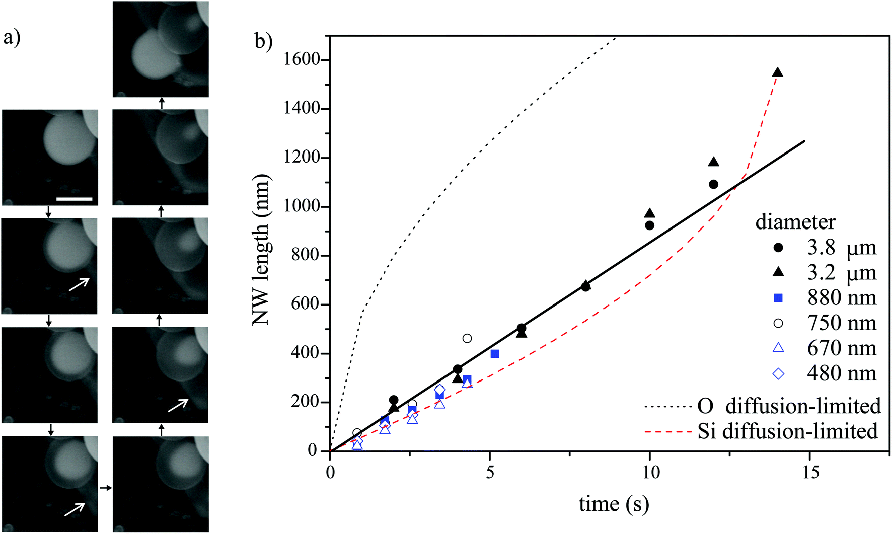 | ||
Fig. 2 Real-time in situ SEM observation of NW shell growth under a dry oxidizing atmosphere and associated growth kinetics. (a) Image sequence obtained from a movie in 2 second steps, showing a disappearing Ga core (bright droplet) and a growing NW shell, as well as Ga expelled from the droplet (marked by the white arrows) during growth; scale bar, 2 μm. (b) Dependence of the NW shell thickness on time at 860 °C for different initial droplet sizes and different oxidizing gases (scattered datapoints). Blue and black symbols represent data from experiments performed under oxygen and nitrogen atmospheres, respectively. The lines are fits (diffusion length calculated as  ) to the experimental data from the 3.2 μm droplet (filled triangles) obtained using a diffusion-driven growth model – the black dotted line represents the oxygen-diffusion-limited regime (assuming a diffusion coefficient, D, of 3.2 × 10⁻⁹ cm2 s−1 for oxygen in SiO2 at 860 °C),43 the red dashed line represents the silicon-diffusion-limited regime (assuming that D = 1.4 × 10⁻⁹ cm2 s−1 for silicon diffusion in liquid Ga, which is in this case one order of magnitude lower than the value reported for 450 °C).44 Note that the curves simulated for the oxygen and silicon-limited regimes have sublinear and superlinear dependencies on time, respectively, since the oxygen atom travel distance to the nucleation point increases as the NWs grow, while that of the silicon atoms decreases because of the shrinking gallium core. ) to the experimental data from the 3.2 μm droplet (filled triangles) obtained using a diffusion-driven growth model – the black dotted line represents the oxygen-diffusion-limited regime (assuming a diffusion coefficient, D, of 3.2 × 10⁻⁹ cm2 s−1 for oxygen in SiO2 at 860 °C),43 the red dashed line represents the silicon-diffusion-limited regime (assuming that D = 1.4 × 10⁻⁹ cm2 s−1 for silicon diffusion in liquid Ga, which is in this case one order of magnitude lower than the value reported for 450 °C).44 Note that the curves simulated for the oxygen and silicon-limited regimes have sublinear and superlinear dependencies on time, respectively, since the oxygen atom travel distance to the nucleation point increases as the NWs grow, while that of the silicon atoms decreases because of the shrinking gallium core. | ||
Real-time microscopy allows us to quantify the nanowire growth rate using image sequences similar to that shown in Fig. 2a. The NW length is approximated by the distance between the outer surface of the shell and the shrinking Ga core (i.e. the thickness of the nanowire shell). The dependence of the nanowire length on time is shown in Fig. 2b for nanowires grown from Ga droplets of different sizes at 860 °C under both dry oxygen and nitrogen gas. The NW growth rate is not limited by the supply rate of oxygen molecules since the growth rate is the same under both oxygen and nitrogen atmospheres (and the latter contained only a trace amount of oxygen). The growth rate is nearly constant (i.e. the NW length scales linearly with time as shown by the straight line in Fig. 2b). Therefore, it is neither limited by oxygen diffusion along the growing NWs nor by silicon diffusion through the gallium droplet, both of which would have shown the  dependencies illustrated by dotted and dashed curves in Fig. 2b. Additionally, the latter scenario, i.e. silicon diffusion limited process, is inconsistent with the fact that the growth rate is independent of the initial size of the Ga droplet (within the range studied in our experiments). Hence, the growth rate is likely limited by (i) the reaction rate (Si oxidation) or (ii) the supply rate of oxygen via diffusion through the gallium oxide shell. The results in Fig. 2 cannot be used to deduce unambiguously the rate-limiting mechanism. However, additional experiments will be discussed below to show that scenario (ii) is more likely. Additionally, scenario (ii) is consistent with the subtle increase in the growth rate observed during the later stages of growth in several experiments (e.g. see Fig. 2b, data for Ga droplets with a diameter of 3.2 μm) due to gallium oxide shell thinning caused by water-assisted etching. The Arrhenius analysis of growth rates measured at different temperatures enables determination of the corresponding activation energy (see ESI S7†).
3.2 NW growth under a wet atmosphere
Fig. 1 indicates that growth induced by a wet oxidant (water vapor) is strikingly different. Nanowires grow outwards from the catalyst droplets, forming dense wool-like patterns. Fig. 3a shows an image sequence of growth from a Ga droplet at 410 °C under 200 Pa of water vapor. Here, the quantitative analysis of the growth rate is less straightforward due to the stranded nanowire morphology, but key features of the growth process can still be derived from the experiment. Nanowire growth is initially accompanied by shrinkage of the Ga core, similar to the case of growth under a dry atmosphere. However, during the later stages of growth, the gallium core ceases to shrink and nanowire bunches spread outwards from the Ga droplet. Notably, the oxide shell becomes detached from the Ga catalyst (marked by the arrows in Fig. 3a). Images of numerous growth products suggest that the gallium oxide shell is either etched away completely during growth (see Fig. 1f) or etched sufficiently to break up and detach from the catalyst droplet (Fig. 3a, ESI Fig. S4d†). After some time, growth terminates (at ∼342 s in the case documented in Fig. 3a) and does not resume. The growth termination is accompanied by a change in catalyst droplet image contrast.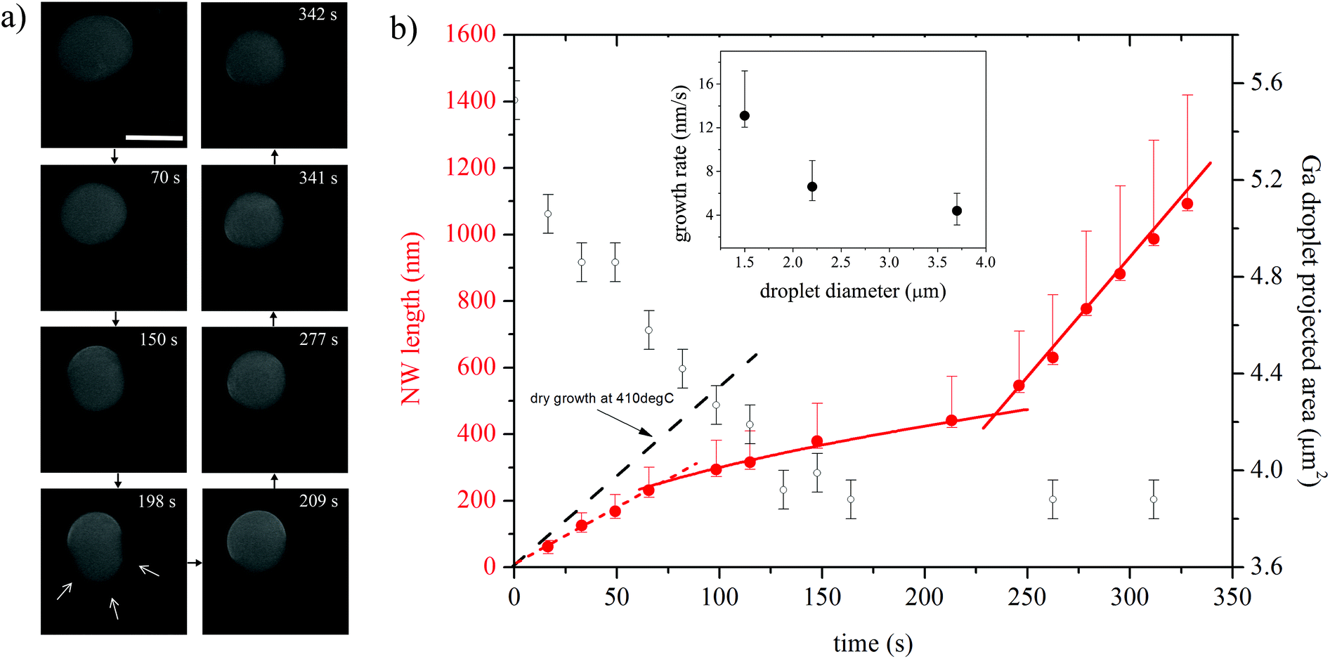 | ||
| Fig. 3 Real-time in situ SEM observation of NW growth under a wet oxidizing atmosphere at 410 °C under 200 Pa of water vapor. (a) Shortly after introduction of water vapor, the Ga core shrinks. The nanowires nucleate and grow towards the core (70 s). Subsequently, nanowire bunches grow outwards from the Ga catalyst, connected with what is possibly the remnant of the oxide shell (marked by the white arrows). The growth terminates at ∼342 s and the Ga core abruptly becomes darker in the image (see images taken at 341 and 342 s); scale bar, 2 μm. (b) Dependence of the NW growth rate on time at 410 °C for a Ga catalyst with an initial diameter of 2.6 μm (different from the one shown in (a)). The dashed black line shows the growth rate dependence measured at the same temperature under a dry atmosphere (ESI S7†), while the red curves show three distinct stages of growth. The open circles show the calculated projected Ga catalyst area. Inset: dependence of the nanowire growth rate on the Ga core diameter measured during the final (third) stage of growth. | ||
The quantitative analysis of growth under a wet atmosphere is limited by relatively large uncertainties in NW lengths estimated from real-time SEM images. Nevertheless, correlation of the data with ex situ high-resolution SEM images enables assessment of the uncertainties and analysis of the data as shown in Fig. 3b. Growth under a wet atmosphere proceeds in three stages: (i) initially, the growth rate is constant, (ii) subsequently the growth rate significantly decelerates, and eventually (iii) rapidly accelerates. During stage (i) the gallium core shrinks as can be seen from the calculated projected Ga catalyst area shown in Fig. 3b, but the rate of shrinkage significantly decreases during stage (ii). The core dimensions (and volume) do not change during stage (iii). Hence, similar to growth under a dry atmosphere, the NWs initially nucleate at the Ga/gallium oxide interface and grow towards the core. The initial growth rate is very similar to that under a dry atmosphere (see the dashed line in Fig. 3b), suggesting that it is limited by diffusion of water molecules through the gallium oxide shell, and that the associated diffusivity is similar under both atmospheres. The growth rate subsequently decreases and shows a sub-linear diffusion-limited behavior, indicating that the growth is limited by diffusion of water molecules along the NWs. The rapid increase of the growth rate in stage (iii) is related to the detachment of the remnants of the gallium oxide shell. Water molecules do not diffuse along the NWs to the growth interface anymore, but are instead supplied directly from the gas phase.47 In this growth regime the growth rate depends inversely on the gallium droplet size (see inset of Fig. 3b) which indicates that the growth is now limited by silicon diffusion through the Ga catalyst.
3.3 Gallium oxide decomposition
Although the final morphology of NWs grown under dry and wet atmospheres is strikingly different, our analysis shows that the underlying mechanisms are very similar and the main difference is the presence/absence of the gallium oxide shell and its attachment/detachment with respect to the Ga droplet during the later stages of growth. To elucidate the shell decomposition mechanism we characterized the oxide shell after exposure to dry oxygen and water vapor at elevated temperatures by in situ XPS (see the Experimental section). The evolution of the Ga 2p peak during annealing in dry oxygen (Fig. 4a) shows that the gallium oxide shell remains intact up to a very high temperature (860 °C). Conversely, annealing in water vapor causes significant oxide reduction, even at temperatures as low as 320 °C, and the disappearance of the gallium oxide-related photoelectron peak is accompanied by an increase in the intensity of the metallic Ga peak. The low-temperature oxide reduction is surprising since Ga2O3 is very stable up to high temperatures.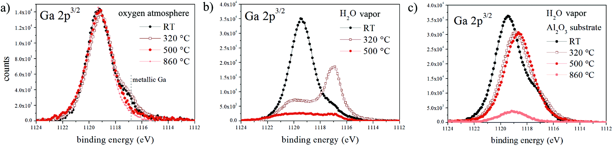 | ||
| Fig. 4 In situ XPS analysis of the gallium oxide shell after exposure to different atmospheres at different temperatures. (a) In pure oxygen, the oxide shell remains intact at annealing temperatures of 320, 500 and 860 °C. The intensity of the metallic Ga peak decreases at high temperatures due to oxide growth during annealing. (b) In water vapor, the oxide-related peak and metallic Ga peak decreases and increases, respectively, due to decomposition of gallium oxide at temperatures as low as 320 °C. (c) Importantly, annealing of oxide-encapsulated Ga droplets in water vapor on an alumina substrate does not result in decomposition of the gallium oxide shell at 320 or 500 °C, highlighting the critical role of silicon in the decomposition process. | ||
Gallium oxide is known to be reduced by molecular hydrogen via the following reactions:
| Ga2O3 + 3H2 → 2Ga + 3H2O, |
| Ga2O3 + 2H2 → Ga2O + 2H2O. | (1) |
Indeed, we have also observed gallium oxide decomposition under a hydrogen atmosphere (similar to Fig. 4b, not shown here). However, there is no obvious source of hydrogen in our experimental setup, particularly in the UHV cluster tool where the partial pressure of hydrogen is extremely low. A possible pathway for the generation of hydrogen is the silicon oxidation reaction at an elevated temperature:
| Si + 2H2O → SiO2 + 2H2. | (2) |
To prove that silicon substrates play a role in the gallium oxide decomposition process, we prepared oxide-encapsulated Ga droplets on a Si substrate coated by 20 nm of Al2O3. Fig. 4c clearly shows that in water vapor the gallium oxide undergoes a significant decomposition only at temperatures higher than 500 °C (the peak shift is indicative of a stoichiometric change towards Ga suboxides). Therefore, we conclude that silicon substrates act as catalysts for the decomposition of H2O through reaction (2), generating H2 that subsequently etches the gallium oxide shell during NW growth under a wet atmosphere.
3.4 Growth mode discussion
Our experiments show that the liquid–metal droplet mediates the diffusion of silicon to the growth front located at the droplet/NW interface. The oxidizing species arrive from the vapor phase and are dissolved in the catalyst48,49 where they react with Si (supplied from the solid phase via the solid–liquid interface). This implies that the oxidation of dissolved silicon must be preferred over catalyst oxidation. This condition is satisfied if the Gibbs free energy of the formation of the dissolved oxide is low compared to that of the metal droplet oxide (e.g. for silicon oxide it is very low compared to gallium oxide).50Next, it is instructive to consider why the nanowires initially nucleate below the gallium oxide shell (Fig. 5a). Based on simple thermodynamic arguments nucleation is expected to be preferred on the outer surface of the gallium oxide (nucleus (i), Fig. 5), rather than the inner surface (nucleus (ii)), because of the very low surface free energy of silicon oxide (250–500 mJ m−2 compared to the Ga/SiO2 interface energy of 785 mJ m−2).26,51 However, our experiments indicate that nucleation at site (i) is limited by silicon diffusion through the gallium oxide shell. Hence, there are two interfaces where nucleation is likely – at the gallium oxide shell/Ga droplet interface (nucleus (ii)) or at the substrate/Ga droplet interface (nucleus (iii)). The Gibbs free energy change for these two cases is, however, similar (the surface free energies of Ga/Ga2O3 and Ga/Si interfaces are both between 0.7 and 0.8 mJ m−2).26,52 Hence, there should be no preferential nucleation site, in contrast to our observation that nucleation is preferred below the oxide shell. We therefore conclude that the gallium oxide shell effectively lowers the energy barrier for the formation of SiOx nuclei at position (ii). This is supported by the experimental observation that oxide NWs do not nucleate if the oxide shell is absent initially or during later stages of growth (ESI, Fig. S4d†). It is noteworthy that the solubility of oxygen in Ga is a few orders of magnitude lower than that of Si.53 Hence, supersaturation of Ga by SiOx species occurs preferentially near the liquid–oxide shell interface, which highlights its importance as a preferential nucleation interface.14,54
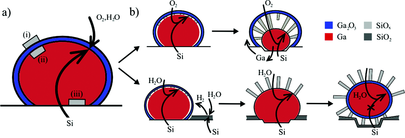 | ||
| Fig. 5 Schematic illustration of preferential nucleation (a) and material supply pathways (b) for silicon oxide nanowire growth under dry and wet oxidizing atmospheres. (a) Initial nucleation occurs at the liquid Ga/oxide shell interface (nucleus (ii)), minimizing the energy increase of the system. (b) In the case of dry oxidation (top) the gallium oxide shell is preserved and growth terminates if Ga is fully expelled from the droplet or if the outward flow of Ga is not possible. In the presence of water (or if hydrogen is supplied from an external source) the gallium oxide shell is etched away (bottom). Growth is fed by diffusion of the growth species to the nanowire base, and terminates if the Ga droplet is detached from the substrate. However, this can be prevented if the droplet moves across the surface (ESI S8†), which results in almost unlimited supply of the growth material. | ||
NW growth under a dry atmosphere is illustrated schematically in Fig. 5b (top). Silicon atoms are supplied from the substrate and the growth rate is limited kinetically by diffusion of oxygen through the gallium oxide shell. Oxygen transport through the shell is mediated by the porous nature of the gallium oxide.55 The growth front is at the NW–Ga interface and NW growth proceeds via attachment of the growth species to the nanowire base.
Nanowire growth in the presence of water vapor is mechanistically similar (Fig. 5b) during the initial stage of growth. However, the gallium oxide shell is continuously etched via reaction (1) by hydrogen generated through reaction (2). This explains why nanowires grow away from the catalyst surface, and not towards the core. The nanowires are no longer pinned to the gallium oxide shell and can therefore bend easily due to attractive forces56,57 and form bunches (compared to those grown under the oxide shell).
Because the silicon substrate is readily oxidized by water at elevated temperatures, the Ga catalyst comes into contact with the growing silicon oxide. Gallium is known to decompose silicon dioxide58via the following reactions:
| 2Ga + SiO2 → SiO + Ga2O, |
| 4Ga + SiO2 → Si + 2Ga2O. | (3) |
The gallium suboxide is decomposed by hydrogen, and gallium in the droplet is therefore not consumed during nanowire growth (in agreement with the experimental data shown in Fig. 3). Clearly, the reactions between gallium and silica show that the nanowires cannot be composed of pure SiO2. Instead, non-stoichiometric oxides (SiOx, x < 2) which are not soluble in Ga were detected (ESI S1 and S3†), as in prior studies.18,23–25,33,34
If a Ga droplet loses contact with the silicon substrate, nanowire growth terminates because the Si supply path is broken and the Ga collector becomes depleted of silicon. This usually happens if the Ga droplet is elevated by a dense batch of nanowires (see ESI, Fig. S4 and S8b†). Oxidation of the underlying silicon substrate is no longer prevented by reaction (3) and local hydrogen formation via reaction (2) also decelerates (due to the absence of a Si surface). Consequently, the formation of a gallium oxide shell on the Ga surface is promoted via water-induced oxidation. This is supported by the observed rapid change in Ga droplet contrast in SEM images (Fig. 3 and ESI, Fig. S8†) after growth termination, attributed to a change in the secondary electron yield caused by gallium oxide formation. Interestingly, real-time SEM revealed that, small Ga droplets are mobile under a wet atmosphere, and that the droplets continue to promote NW growth as they traverse the substrate (see ESI S8†). The movement acts to sustain reaction (3) because mobile droplets consume the silicon oxide along their paths. Finally, we note that immobile catalyst droplets can consume significant amounts of the underlying substrate material (see ESI, Fig. S4†) via reactions (2) and (3).
Our model of growth under a water-containing atmosphere is applicable to numerous prior silicon oxide nanowire growth studies. Typically, hydrogen-containing carrier gases or precursors are used,24,25,33,34 which effectively etch the gallium oxide yielding growth product morphologies that are similar to those observed here. Additionally, H2O is a common impurity present as a gas contaminant or introduced through leaks in the system,24,25,33 and is an additional source of hydrogen. If Si vapor or Si-containing molecules are supplied to the sample, nanowire growth does not cease when droplets detach from the substrate because the growth is fed by the Si atoms from the vapor, resulting in the “floating catalyst” morphology.25,26,33,35 In the absence of hydrogen, the gallium oxide shell is present and the nanowires grow towards the catalyst core.22,23
4. Conclusions
We have demonstrated the critical role of gallium oxide in the growth of silicon oxide nanowires using liquid gallium catalyst droplets. The gallium oxide can decompose during growth, and thus alter the growth kinetics and nanowire morphology. The decomposition is caused by hydrogen which gives rise to etching, and can be supplied via thermal dissociation of H2O, a common impurity in CVD systems. The dissociation of H2O is catalyzed by silicon substrates at temperatures as low as 320 °C. We presented a detailed model of nanowire growth that accounts for both H-containing and H-free environments.Acknowledgements
The authors acknowledge J. Čechal and P. Varga for critical reading of the manuscript. This work was supported by the Grant Agency of the Czech Republic (P108/12/P699) and by the European Regional Development Fund – (CEITEC – CZ.1.05/1.1.00/02.0068). M. K. acknowledges the support of FEI Company.References
- Y. Cui and C. M. Lieber, Science, 2001, 291, 851 CrossRef CAS PubMed.
- C. Thelander, P. Agarwall, S. Brongersma, J. Eymery, L. F. Feiner, A. Forchell, M. Scheffler, W. Riess, B. J. Ohlsson, U. Gösele and L. Samuelson, Mater. Today, 2006, 9, 28 CrossRef CAS.
- H. Yan, H. S. Choe, S. Nam, Y. Hu, S. Das, J. F. Klemic, J. C. Ellenbogen and C. M. Lieber, Nature, 2011, 470, 240 CrossRef CAS PubMed.
- H. Riel, L.-E. Wernersson, M. Hong and J. A. del Alamo, MRS Bull., 2014, 39, 668 CrossRef CAS.
- Y. Tao, E. Ju, J. Ren and X. Qu, Adv. Mater., 2015, 27, 1097 CrossRef CAS PubMed.
- M.-S. Hu, H.-L. Chen, C.-H. Shen, L.-S. Hong, B.-R. Huang, K.-H. Chen and L.-C. Chen, Nat. Mater., 2006, 5, 102 CrossRef CAS PubMed.
- S. Mukherjee, L. Zhou, A. M. Goodman, N. Large, C. Ayala-Orozco, Y. Zhang, P. Nordlander and N. J. Halas, J. Am. Chem. Soc., 2014, 136, 64 CrossRef CAS PubMed.
- A. Rao, A. Bankar, A. Shinde, A. R. Kumar, S. Gosavi and S. Zinjarde, ACS Appl. Mater. Interfaces, 2012, 4, 871 CAS.
- E. Murphy-Perez, S. K. Arya and S. Bhansali, Analyst, 2011, 136, 1686 RSC.
- N. S. Ramgir, A. Zajac, P. K. Sekhar, L. Lee, T. A. Zhukov and S. Bhansali, J. Phys. Chem. C, 2007, 111, 13981 CAS.
- P. K. Sekhar, N. S. Ramgir and S. Bhansali, J. Phys. Chem. C, 2008, 112, 1729 CAS.
- A. Kausnik, R. Kumar, E. Huey, S. Bhansali, N. Nair and M. Nair, Microchim. Acta, 2014, 181, 1759 CrossRef.
- L. Tong, J. Lou, R. R. Gattass, S. He, X. Chen, L. Liu and E. Mazur, Nano Lett., 2005, 5, 259 CrossRef CAS PubMed.
- B. A. Wacaser, K. A. Dick, J. Johansson, M. T. Borgström, K. Deppert and L. Samuelson, Adv. Mater., 2009, 21, 153 CrossRef CAS.
- V. Schmidt, J. Wittemann and U. Gösele, Chem. Rev., 2010, 110, 361–388 CrossRef CAS PubMed.
- H. F. Yan, Y. J. Xing, Q. L. Hang, D. P. Yu, Y. P. Wang, J. Xu, Z. H. Xi and S. Q. Feng, Chem. Phys. Lett., 2000, 323, 224 CrossRef CAS.
- C.-Y. Wang, L.-H. Chan, D.-Q. Xiao, T.-C. Lin and H. C. Shih, J. Vac. Sci. Technol., B, 2006, 24, 613 CAS.
- B. Zheng, Y. Wu, P. Yang and J. Liu, Adv. Mater., 2002, 14, 122 CrossRef CAS.
- G. A. Bootsma and H. J. Gassen, J. Cryst. Growth, 1971, 10, 223 CrossRef CAS.
- M. K. Sunkara, S. Sharma, R. Miranda, G. Lian and E. C. Dickey, Appl. Phys. Lett., 2001, 79, 1546 CrossRef CAS.
- Z. W. Pan, Z. R. Dai, C. Ma and Z. L. Wang, J. Am. Chem. Soc., 2002, 124, 1817 CrossRef CAS PubMed.
- L. Dai, L. P. You, X. F. Duan, W. C. Lian and Q. Q. Qin, Phys. Lett. A, 2005, 335, 304–309 CrossRef CAS.
- P. A. Hu, Y. Q. Liu and X. B. Wang, Appl. Phys. A, 2003, 77, 743–745 CrossRef CAS.
- S. Luo, W. Zhou, W. Chu, J. Shen, Z. Zhang, L. Liu, D. Liu, Y. Xiang, W. Ma and S. Xie, Small, 2007, 3, 444–450 CrossRef CAS PubMed.
- X. Q. Yan, W. Y. Zhou, L. F. Sun, Y. Gao, D. F. Liu, J. X. Wang, Z. P. Zhou, H. J. Yuan, L. Song, L. F. Liu, G. Wang and S. S. Xie, J. Phys. Chem. Solids, 2005, 66, 701–705 CrossRef CAS.
- M. Bettge, S. MacLaren, S. Burdin, D. Abraham, I. Petrov, M.-F. Yu and E. Sammann, J. Mater. Res., 2011, 26, 2247 CrossRef CAS.
- P. Wu, X. Zou, L. Chi, Q. Li and T. Xiao, Nanotechnology, 2007, 18, 125601 CrossRef.
- R. Ma and Y. Bando, Chem. Phys. Lett., 2003, 377, 177–183 CrossRef CAS.
- X. M. Cai, A. B. Djuriši and M. H. Xie, J. Appl. Phys., 2005, 98, 074313 CrossRef.
- J. Zhang, Y. Yang, S. Ding, J. Li and X. Wang, Mat. Sci. Eng., B, 2008, 150, 180–186 CrossRef CAS.
- J. Zhang, F. Jiang, Y. Yang and J. Li, J. Cryst. Growth, 2007, 307, 76 CrossRef CAS.
- J. Qu, Z. Zhao, X. Wang, J. Qiu and Y. Gogotsi, Mater. Exp., 2012, 2, 157 CrossRef CAS.
- Z. Pan, S. Dai, D. B. Beach and D. H. Lowndes, Nano Lett., 2003, 3, 1279–1284 CrossRef CAS.
- X. Zhang, Z. Liu, Z. Zheng and S. Hark, J. Mater. Res., 2008, 23, 1667 CrossRef CAS.
- Z. Gu, F. Liu, J. Y. Howe, M. Parans Paranthaman and Z. Pan, Nanoscale, 2009, 1, 347 RSC.
- H. F. Yan, Y. J. Xing, Q. L. Hang, D. P. Yu, Y. P. Wang, J. Xu, Z. Xi and S. Q. Feng, Chem. Phys. Lett., 2000, 323, 224–228 CrossRef CAS.
- I. Aharonovich, Y. Lifshitz and S. Tamir, Appl. Phys. Lett., 2007, 90, 263109 CrossRef.
- D. Zhang and R. Q. Zhang, J. Phys. Chem. B, 2006, 110, 1338 CrossRef CAS PubMed.
- M. Kolibal, T. Cechal, E. Brandejsova, J. Cechal and T. Sikola, Nanotechnology, 2008, 19, 475606 CrossRef PubMed.
- D. Drouin, A. R. Couture, D. Joly, X. Tastet, Z. Aimez and R. Gauvin, Scanning, 2007, 29, 92 CrossRef CAS PubMed.
- H. Chandrasekaran, G. U. Sumanasekara and M. K. Sunkara, J. Phys. Chem. B, 2006, 110, 18351 CrossRef CAS PubMed.
- F. M. Ross, Rep. Prog. Phys., 2010, 73, 114501 CrossRef.
- K. Kajihara, T. Miura, H. Kamioka, M. Hirano, L. Skuja and H. Hosono, J. Ceram. Soc. Jpn., 2004, 112, 559 CrossRef CAS.
- H. Ogawa, Q. Guo and K. Ohta, J. Cryst. Growth, 1995, 155, 193 CrossRef CAS.
- S. Kodambaka, C. Ngo, J. Palisaitis, P. H. Mayrhofer, L. Hultman and P. O. A. Persson, Appl. Phys. Lett., 2013, 102, 161601 CrossRef.
- W. Liang, L. Hong, H. Yang, F. Fan, Y. Liu, H. Li, J. Li, J. Y. Huang, L.-Q. Chen, T. Zhu and S. Zhang, Nano Lett., 2013, 13, 5212 CrossRef CAS PubMed.
- O. A. Louchev, Y. Sato and H. Kanda, Appl. Phys. Lett., 2002, 80, 2752 CrossRef CAS.
- H. Y. Dang, J. Wang and S. S. Fan, Nanotechnology, 2003, 14, 738 CrossRef CAS.
- L. Yu, B. O'Donnell, P. J. Alet, S. Conesa-Boj, F. Peiro, J. Arbiol and P. Roca i Cabarrocas, Nanotechnology, 2009, 20, 225604 CrossRef PubMed.
- T. B. Reed, Free Energy of Formation of Binary Compounds: An Atlas of Charts for High-Temperature Chemical Calculations, The MIT Press, Cambridge, Mass, 1971 Search PubMed.
- Y. I. Tarasevich, Theor. Exp. Chem., 2006, 42, 145 CrossRef CAS.
- S. Conesa-Boj, I. Zardo, S. Estrade, L. Wei, P. J. Alet, P. Roca i Cabarrocas, J. R. Morante, F. Peiro, A. Fontcuberta i Morral and J. Arbiol, Cryst. Growth Des., 2010, 10, 1534 CAS.
- C. B. Alcock and K. T. Jacob, J. Less. Common Met., 1977, 53, 211 CrossRef CAS.
- K. W. Kolasinski, Curr. Opin. Solid State Mater. Sci., 2006, 10, 182 CrossRef CAS.
- A. Plech, U. Klemradt, H. Metzger and J. Peisl, J. Phys.: Condens. Matter, 1998, 10, 971 CrossRef CAS.
- C. N. Cochran and L. M. Foster, J. Electrochem. Soc., 1962, 109, 149 CrossRef CAS.
- Z. Sun, D. Wang and J. Xiang, ACS Nano, 2014, 8, 11261 CrossRef CAS PubMed.
- M. Khorasaninejad, N. Abedzadeh, A. S. Jawanda, O. Nixon, M. P. Anantram and S. S. Saini, J. Appl. Phys., 2012, 111, 044328 CrossRef.
Footnote |
| † Electronic supplementary information (ESI) available: Additional nanowire analysis (Fig. S1–S4), real-time EDX analysis of the Si content in the Ga droplet (Fig. S5), image sequence S6 showing crack formation and further evolution of the catalyst droplet morphology, determination of the activation energy of NW formation (Fig. S7), and a demonstration of Ga droplet migration (Fig. S8). See DOI: 10.1039/c5nr05152e |
| This journal is © The Royal Society of Chemistry 2016 |