
Low temperature formation of rectangular PbTe nanocrystals and their thermoelectric properties
U.
Nithiyanantham
a,
M. Fevzi
Ozaydin
b,
Abdullah S.
Tazebay
b and
Subrata
Kundu
*a
aElectrochemical Materials Science (ECMS), CSIR-Central Electrochemical Research Institute (CECRI), Karaikudi 630006, Tamil Nadu, India. E-mail: skundu@cecri.res.in; kundu.subrata@gmail.com; Fax: +91-4565-227651; Tel: +91-4565-241487
bMaterials Science and Mechanical Engineering, Texas A&M University, College Station, TX 77843-3123, USA
First published on 15th October 2015
Abstract
We report a low-temperature route for the successful generation of rectangular PbTe nanocrystals (NCs) within a short time under continuous heating at 80 °C. The PbTe NCs are formed by the reaction of Te metal powder with Pb-acetate salt in the presence of alkaline 2,7-DHN solution in a CTAB micellar medium. Two different sizes of rectangular PbTe NCs were synthesized just by tuning the CTAB to metal salt precursor molar ratio and controlling other reaction parameters. The optical properties, thermal stability and electronic properties of the PbTe NCs were studied in detail utilizing various instrumental techniques. The growth mechanism for the formation of the rectangular PbTe NCs has been elaborated. Both of the morphologies were tested for their application as thermoelectric (TE) materials. It was observed that both sizes of rectangular PbTe NC could be used as thermoelectric materials and among the two morphologies, the small sized rectangular PbTe NCs showed the maximum TE figure of merit (ZT) value compared to the larger size at 475 K. The high ZT value of the smaller sized rectangular PbTe NCs in comparison to the larger size ones is due to their higher power factor value, as well as their low thermal conductivity value compared to the large sized PbTe NCs. Other than power generation, the synthesized PbTe NCs may be further used in electrochemical biosensors and nano-optoelectronic devices and to improve the light-use efficiency of solar devices.
Introduction
Thermoelectric (TE) technology includes power generation and electronic refrigeration. Thermoelectricity is a phenomenon describing the direct conversion of heat into electricity. A typical thermoelectric device consists of p- and n-type TE materials and has many advantages, such as no moving part, no noise, they contain no chlorofluorocarbons and have a long life time of reliable operation. Among these materials, n-type materials serve as the electron charge carriers with negative Seebeck coefficient values and p-type materials contain holes as the charge carriers with positive Seebeck coefficient values. Therefore, increasing attention has been turned to TE materials with high TE efficiency over the last few years. Nevertheless, due to their low efficiencies, current TE materials have found limited commercial applications. The efficiency or performance of a TE material is denoted by the dimensionless figure of merit (ZT): ZT = S2σT/k where, S is the Seebeck coefficient, σ is the electrical conductivity, k is the thermal conductivity and T is the absolute temperature in Kelvin.1 In order to get high TE efficiency or to increase the ZT, a high Seebeck coefficient, low thermal conductivity and high electrical conductivity are necessary.2 It becomes a real challenge to enhance the ZT value as the materials properties S, σ, k will all affect each other, making an optimization process necessary. Usually in TE processes, the carriers diffuse towards the cold side and generate a thermoelectric voltage, while temperature gradients are present in the TE systems. The main advantage of nanostructured TE modules is their lattice contributions to the thermal conductivity. In nanoscale regimes, heat-carrying phonons are scattered by introducing a large number of grain boundaries into the nanomaterials.Among the different types of TE materials studied so far, lead telluride (PbTe), an important group IV–VI semiconductor with a narrow band gap of ∼0.21 eV and a face-centered cubic (fcc) structure,3 is one of the most commonly used materials for solid-state TE cooling and electrical power generation devices that can operate at medium temperatures of 450–800 K.4 Nanoscale materials are expected to generate better TE efficiencies compared to their bulk counterparts due to their large surface to volume ratios. It is reported that two-dimensional thermoelectric materials, especially nanowires, nanotubes and super-lattices, have shown improved ZT values due to the quantum confinement effect, a sharper density of states for enhanced thermopower and strong phonon boundary scattering for reduced lattice thermal conductivity.5 PbTe TE materials have been extensively studied since they exhibit high structural and chemical stabilities and low vapour pressures at operating temperatures ranging from 50 °C to 600 °C. A variety of routes have been proposed for the synthesis of PbX (X = S, Se, Te) nanomaterials including templated synthesis in mesoporous silica channels,6 the oriented attachment of nanoparticles (NPs),7 seeded solution synthesis,8 colloidal synthesis9 and solvothermal,10 hydrothermal11 and chemical vapour transport (CVT) routes.12 Additionally, different interesting structures like NPs,13 nanorods or nanowires14 and nanotubes15 have been synthesized utilizing different chemical and physical routes. Size-controlled monodispersed PbTe quantum dots were synthesized by Pan et al. using oleylamine as a capping ligand.16 Size and shape-selective PbTe NCs were synthesized by Mokari et al. at a high temperature of 250 °C.17 Low dimension PbTe NCs were synthesized by Murphy et al. at 170 °C under an inert atmosphere.18 Hu et al. synthesized PbTe nanotubes utilizing a thermal chemical reaction process.19 Chen et al. synthesized aggregated PbTe nanomaterials utilizing a gas-induced reduction process at 348 K for 24 hours.20 Fardy et al. prepared PbTe chalcogenide nanowires under an inert atmosphere at high temperature.1 Papageorgiou et al. prepared n-type PbTe NCs at 430 °C.21 The sonochemical synthesis of nanocrystalline PbTe with Pb as an impurity has been reported by Li et al. using Pb-acetate and Te powder as the precursors after an 8 hour reaction.22 Tai et al. prepared PbTe nanowires using Te nanowires as the template utilizing a hydrothermal process at 180 °C for 24 hours.23 Zhou et al. prepared flower-like PbTe nanomaterials under hydrothermal conditions using Pb-acetate and Na2TeO3 precursors at 240 °C for 24 hours.24 Zhu et al. prepared PbTe nanosheets using hydrothermal conditions through the reaction of Pb-nitrate with Na2TeO3 and NaBH4 at high temperature.25 Hierarchical superstructures of lead chalcogenides were prepared by a microwave assisted method with Pb-acetate and tellurium powder in ethylene glycol.26 There are a few other methods reported for the successful formation of PbTe nanomaterials utilizing various synthetic routes.27–29 It is accepted that the presence of a stabilizing agent can affect the final morphology of the nanomaterials to a great extent. Different stabilizing or capping agents had been utilized for the successful growth and formation of PbTe nanomaterials such as sodium dodecyl sulphate (SDS),30 polyethylene glycol (PEG),31 polyvinyl pyrrolidine (PVP)32 and different ionic liquids, etc. Most of the above methods require sophisticated precursors, high temperatures, long processing times and expensive chemicals and the final products lack monodispersity resulting in a mixture of shapes or a mixture of precursor metal impurities with the desired nanomaterials. To the best of our knowledge, there is no report on the low temperature (60–80 °C) synthesis of rectangular PbTe NCs within a short reaction time and the morphology dependent study of their TE properties.
In the present study, we highlight for the first time, a low-temperature route for the synthesis of rectangular PbTe NCs at 80 °C within a short reaction time. The PbTe NCs were synthesized by the reaction of Pb-acetate solution with Te metal powder and alkaline 2,7-dihydroxy naphthalene (2,7-DHN) solution in a cetyl trimethyl ammonium bromide (CTAB) micellar medium. Two different sizes of rectangular PbTe NC were formed by tuning the surfactant to metal salt precursor molar ratio and by altering the other reaction parameters. The formation and growth mechanisms of the rectangular PbTe NCs have been elaborated. Both of the morphologies have been utilized for TE applications and it was observed that the rectangular PbTe NCs with the smaller size gave a better ZT value compared to the larger size. The synthesis process is fast, cost-effective, reproducible and may be highly beneficial for industrial scale production due to the use of few reagents and the reduced cost resulting from the simplified low-temperature reaction.
Experimental section
Reagents
Cetyl trimethyl ammonium bromide (CTAB, 99%), lead acetate [Pb(CH3COO)2·2H2O], Te metal powder, 2,7-dihydroxynaphthalene (2,7-DHN) and sodium hydroxide were all purchased from Sigma-Aldrich, India and used as received. A graphite die was used to make the pellets for the TE measurements. De-ionized (DI) water was used for the entire synthetic process.Instruments
The synthesized CTAB–PbTe NCs were characterized with several spectroscopic techniques, including UV-vis, TEM, FE-SEM, AFM, EDS and XRD techniques, as well as thermal and FT-IR analyses, as discussed below. The UV-visible (UV-vis) absorption spectra were recorded using a double beam UV-vis spectrophotometer purchased from Unico (model 4802) equipped with a 1 cm quartz cuvette holder for liquid samples. The Transmission Electron Microscopy (TEM) analysis was performed using a JEOL-JEM 2010 and Tecnai model TEM instrument (TecnaiTM G2 F20, FEI) with an accelerating voltage of 200 kV. The energy dispersive X-ray spectroscopy (EDS) analysis was performed using a Field Emission Scanning Electron Microscopy (FE-SEM) instrument with a separate EDS detector connected to the instrument. The FE-SEM study was done with Zeiss ultra FE-SEM instruments. Dried PbTe powder was directly used for the characterization by X-ray diffraction (XRD) and Fourier Transform Infrared Spectroscopy (FT-IR). The XRD analysis was performed with a scanning rate of 7° min−1 in the 2θ range 15–80° using a Bruker X-ray powder diffractometer (XRD) with Cu Kα radiation (λ = 0.154 nm). The thermal analysis study was recorded on a thermal analyser-simultaneous TGA/DTA instrument with the model name SDT Q600 and the analysis was performed in air. A hot air oven (temperature up to 1000 °C) was used to anneal the samples at a specific temperature. The FT-IR analysis was performed with the Nexus 670 (FTIR) model, Centaurms 10× (Microscope) having a spectral range of 4000 to 400 cm−1 and an MCT-B detector. A magnetic stirrer was purchased from the local Balaji scientific company and used for stirring purposes throughout the entire work. The spark plasma sintering (SPS) process was done using a carver press with an Agilent 6680A DC power supply of 0–5 V, 0–850 A. For the thermal diffusivity measurements, a high speed Xenon lamp-pulse with a pulse width of 400 μs to 600 μs, pulse energy up to 15 J and thermal diffusivity range from 0.01 to 1000 mm2 s−1 was used in the presence of an argon atmosphere. The heat capacity measurements were performed using modulated differential scanning calorimetry (MDSC) methodology and a Q2000 modulated DSC thermal analysis instrument in the temperature range of −180 °C to 725 °C with an accuracy of ±0.1 °C.Low temperature formation of rectangular PbTe NCs
The PbTe NCs were synthesized by the reaction of Pb-acetate with Te metal powder in the presence of alkaline 2,7-DHN in CTAB micellar medium. In a typical synthesis, 15 mL of 0.1 M CTAB was mixed with 0.6 g of Te metal powder, stirred well and heated at 60 °C initially. The solution became cement colored at this stage due to the Te metal powder. Then after 10 minutes, 100 mL of NaOH solution was added and stirring was continued for another 20 minutes. After that, 20 mL of 2,7-DHN solution was added and the reaction temperature was increased to 80 °C under continuous stirring. At this stage the cement color decreased and the solution slowly turned from a light bluish to deep bluish color. Then, continuously 60 mL of Pb-acetate solution was added drop wise. 5 minutes after the addition of Pb-acetate, a brown colored precipitate started to appear. The reaction was continued for a further 30 minutes, then was stopped and cooled at room temperature. The settled precipitate was washed with ethanol and water several times. After, the precipitate was centrifuged at 8000 rpm for 10 minutes to remove any excess surfactant or other chemicals from the reaction product. Finally, the precipitate was collected and dried at 80 °C for two hours. The sample exclusively contained the PbTe NCs with the smaller sized particles. The other morphology was prepared by just tuning the CTAB to metal salt precursor molar ratio and the detailed concentrations of all the reagents, particle sizes, shapes, reaction times and temperatures are clearly elaborated in Table 1. Scheme 1 shows the schematic formation of the PbTe nanomaterials using this simple wet-chemical process.| Set no. | Final conc. of CTAB (M) | Final conc. of Pb(II) acetate solution (M) | Amount of Te metal powder (gm) | Final conc. of 2,7-DHN (M) | Final conc. of NaOH (M) | Color of the solution | Average particles size (nm) |
|---|---|---|---|---|---|---|---|
| 1 | 7.6 × 10⁻⁵ | 1.53 × 10⁻² | 0.6 | 5.12 × 10⁻³ | 1.53 | Light grey color | Side length 390 ± 20 nm, 230 ± 10 nm |
| 2 | 7.6 × 10⁻³ | 1.53 × 10⁻² | 0.6 | 5.12 × 10⁻³ | 1.53 | Light grey color | Side length 260 ± 5 nm, 190 ± 20 nm |
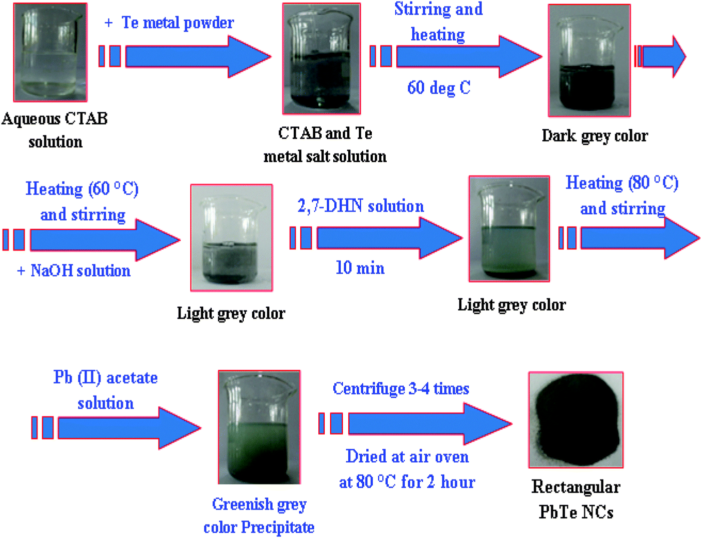 | ||
| Scheme 1 A schematic presentation of the overall preparation process for the formation of PbTe NCs. | ||
Preparation of the synthesized PbTe NCs for thermoelectric measurements
The two differently sized CTAB stabilized rectangular PbTe NCs were tested for their TE performance. The PbTe NCs were prepared in pellet form by loading them into a graphite die and consolidating them with spark plasma sintering (SPS) apparatus at different temperatures. The same amount of each sample was taken and the graphite die was placed in the SPS chamber for sintering. In the SPS process, the PbTe alloys were sintered at 300 °C under 40 MPa of uniaxial pressure for 5 min. The sintering temperature was dependant on the phase diagram of the PbTe. TE measurements were taken below the sintering temperature because this was the safe temperature range at which the specimens would not show any premature melting, thereby entering the mushy zone (solid + liquid). High DC current was passed between the graphite electrodes and axial pressure was simultaneously applied from the beginning of the sintering cycle. Finally, after sample preparation, the materials were analyzed to determine their thermal diffusivity, electrical conductivity, Seebeck coefficient and ZT value, which has been discussed in the following sections.The thermal conductivity (κ) values of the PbTe NCs were evaluated from the thermal diffusivity α, heat capacity Cp and sample density ρ, based on the relationship κ = α·Cp·ρ. The thermal diffusivity was determined via a laser flash method using a flash line 3000 system and the measurements were taken in the temperature range of room temperature (RT) to 1000 °C. In this methodology, one side of the sample with a defined thickness was heated using a short light pulse and the resulting increase in temperature on the other side was detected via a contactless infrared detector. Subsequently, the bulk density of the sample was measured using a standard Archimedes method. The heat capacity was measured using modulated differential scanning calorimetry (MDSC) methodology and a TA instrument Q2000 modulated DSC in the temperature range of −180 to 725 °C with an accuracy of ±0.1 °C. In modulated DSC heat is applied simultaneously and measurements are taken to determine how the rate of heat flow is affected. Compared to standard DSC, modulating the heating rate allows the measurement of both the heat flow that responds to the heating rate (reversing signal) and the heat flow that responds to absolute temperature/time (non-reversing signal). The heat capacity (Cp) is contained within the reversing signal:

Preparation of the samples for characterization
The shape-selective CTAB–PbTe NCs were characterized using UV-vis, TEM, EDS, XRD and XPS techniques, thermal analyses and FT-IR studies. The PbTe NCs obtained after successive centrifugation and drying were used for measurements in the UV-vis spectrophotometer after dispersion in aqueous solution. Solid PbTe powder was mixed with DI water, sonicated for 30 min, and used for TEM sample preparation and other thin film preparations. The TEM samples were prepared by placing a drop of the corresponding PbTe NC solution onto a carbon coated Cu grid followed by slow evaporation of the solvent under ambient conditions. For EDS, XRD and FT-IR analyses, glass slides were used as the substrates for thin film preparation. The slides were cleaned thoroughly in acetone and sonicated for about 30 min. The cleaned substrates were covered with PbTe NC solution and then dried in air. After the first layer was deposited, subsequent layers were deposited by repeatedly adding more PbTe NC solution and drying. The final samples were obtained after 4–5 depositions and then analyzed using the aforementioned techniques. For FE-SEM and AFM, the samples were prepared from the same drop casting method over glass slides but low concentrations were used, unlike those used for XRD and FT-IR. For XPS and TGA/DTA analyses, the as prepared PbTe nanopowders were directly used for the measurements. The sample preparation for the thermoelectric ZT measurements has already been discussed in previous section.Results and discussion
UV-vis spectroscopic analysis
In our present route, the PbTe NCs were synthesized by the reaction of Pb-acetate with Te metal powder in the presence of alkaline 2,7-DHN in CTAB micellar medium. In a typical synthesis, 15 mL of 0.1 (M) CTAB was mixed with 0.6 g of Te metal powder, 100 mL of NaOH solution, 20 mL of 2,7-DHN solution and 60 mL of Pb-acetate solution. Fig. 1 shows the UV-vis absorption spectra of different solution mixtures for the synthesis of the PbTe NCs. Curve a in Fig. 1 shows the absorption band of aqueous CTAB solution alone, which has no specific bands in the UV-vis region. Curve b shows the absorption band of aqueous 2,7-DHN solution alone, which has three distinct absorption peaks at 282 nm, 311 nm and 324 nm. All of these peaks appeared due to the presence of aromatic benzene rings within the structure, as reported earlier.44 Curve c is the absorption band of the Te metal powder in water, which has no distinct absorption bands, but the broad hump peaking near 311 nm might be due to the formation of oxide or hydroxide compounds in water. Curve d is the absorption band of the Pb acetate solution, which has a strong peak at 207 nm and a small hump at 258 nm that might be due to ligand to metal charge transfer (LMCT). Curve e shows the absorption band of a mixture of CTAB, 2,7-DHN, Te metal powder and Pb acetate salt solution, which gives two small absorption bands at 291 nm and 344 nm and a strong peak at 241 nm. These peaks are shifted compared to the pure 2,7-DHN peaks indicating that there is an interaction among the components, possibly the absorption of metal ions onto the positively charged surfactant or the occurrence of a chemical reaction among the components. After completion of the reaction, the product was washed, centrifuged and re-dispersed in aqueous solution. Curves f and g show the absorption bands of the PbTe NCs with the two different morphologies, those with the small sized rectangular PbTe NCs and those with the larger size, respectively. In both of the curves, there are no specific peaks but there are broad humps ranging from 350–760 nm with maxima at 487 nm (small size) and 503 nm (large size). As there are no reports on the electronic absorption spectra of PbTe nanomaterials, we are unable to compare our absorption data with the literature. The peak maxima for both morphologies nicely match with the changes in the absorption band positions with particle size and shape.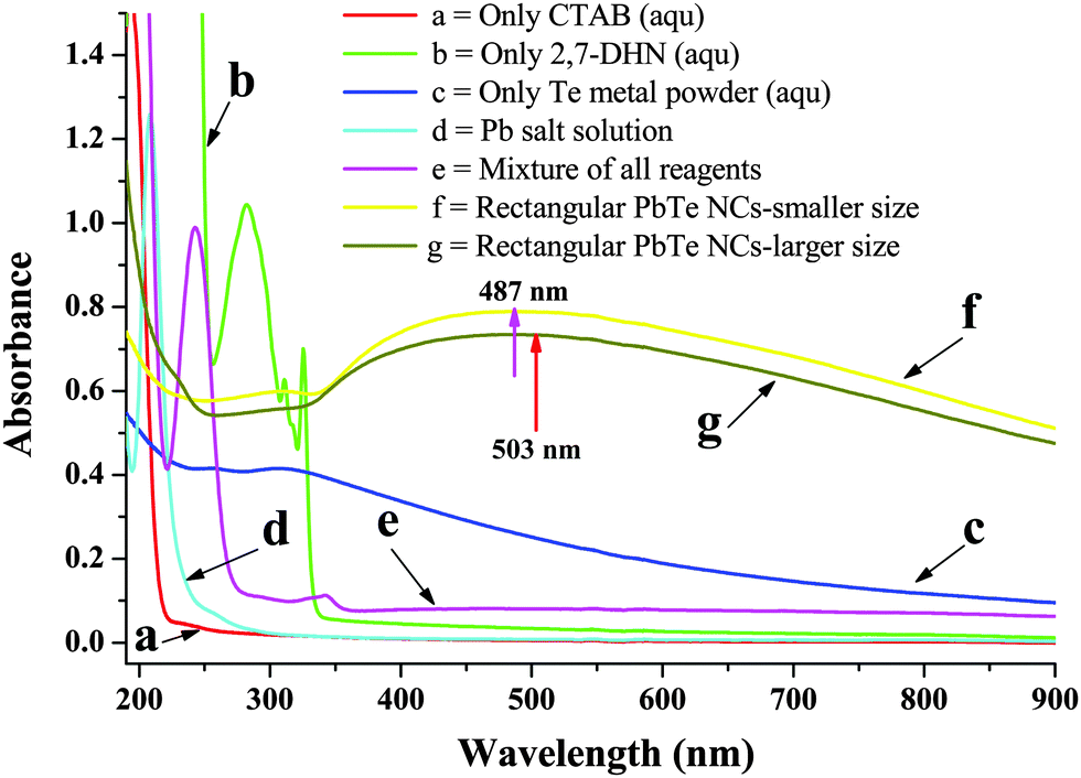 | ||
| Fig. 1 UV-visible absorption spectra of solutions containing different mixtures for the synthesis of PbTe NCs. Curve (a) shows the absorption band of CTAB solution; curve (b) shows the absorption band of aqueous 2,7-DHN solution; curve (c) shows the absorption band of Te metal powder in water; curve (d) shows the absorption band of Pb acetate solution; curve (e) shows the absorption band of the solution containing a mixture of CTAB, 2,7-DHN, Te metal powder and Pb acetate salt solution and curves (f) and (g) show the absorption bands of the PbTe NCs with the two different morphologies, the small sized and large sized rectangular PbTe NCs, respectively. | ||
Morphological analysis using transmission electron microscopy (TEM), field-emission scanning electron microscopy (FE-SEM) and energy dispersive X-ray spectroscopy (EDS)
The transmission electron microscopy (TEM) and field-emission scanning electron microscopy (FE-SEM) images of the PbTe NCs are shown in Fig. 2 and 3, respectively. Fig. 2A and B show the low and high magnification images of the rectangular PbTe NCs with the smaller size, corresponding to curve f in Fig. 1. Fig. 2A is the low magnification image and Fig. 2B is the high magnification image. From the images, the side lengths of the rectangular NCs were calculated. For the smaller sized rectangular PbTe NCs, the side lengths were 260 ± 5 nm (longer side) and 190 ± 20 nm (shorter side). From the images, it is clear that all of the particles formed were almost uniform in size and shape. Fig. 2B shows the image of a single NC. The inset of Fig. 2B shows the corresponding selected area electron diffraction (SAED) pattern, which shows that the particles are crystalline in nature. Clear rectangular diffraction spots are observed in the diffraction pattern indicating the shape effect in SAED. Similar types of shape effect SAED patterns were observed earlier by Kundu et al.41 for the synthesis of triangular Au nanoprisms. Fig. 2C and D show the low and high magnification TEM images of the rectangular PbTe NCs with the larger size, corresponding to curve g in Fig. 1. Fig. 2C is the low magnification image, while Fig. 2D is the image of a single NC. From the image, the average lengths of the rectangular NCs were 390 ± 20 nm (longer side) and 230 ± 10 nm (shorter side). The inset in Fig. 2D shows the corresponding SAED pattern, which shows that the particles are singly crystalline in nature. Here also we have observed a rectangular SAED pattern, as discussed before. From all the TEM images, it is clear that the particles are separated from each other, which might be due to the presence of the stabilizing agent CTAB, which capped the particles on their surface. Similar types of observations have been noticed by others during the synthesis of metal NPs using CTAB and other different organic ligands.33–35 Moreover, in between the particles there is some free surfactant (less contrast) observed, which we were unable to remove by repeated washing and centrifugation. Fig. 3 shows the FE-SEM images of the synthesized rectangular PbTe NCs with the two different morphologies. Fig. 3A shows the high magnification FE-SEM image of the small sized NCs. From the image, it can be seen that all the particles formed perfect rectangular shapes and they aggregated together, either due to the high concentration during sample preparation or due to the slow drying process during water evaporation. The average size of the particles was calculated and matched nicely with the results obtained for the TEM analysis in Fig. 2. Similarly, Fig. 3B shows the FE-SEM image of the rectangular PbTe NCs where the sizes of the particles are large and they also match nicely with the TEM results, as discussed before. So by analysis of the TEM and FE-SEM images, we could confirm that rectangular PbTe NCs were formed in our synthetic process. The energy dispersive X-ray spectroscopy (EDS) analysis of the PbTe NCs (not shown here) consisted of different peaks corresponding to elements such as Pb, Te, C, O and Br, which were present in our synthesized products. The high intensity Pb and Te peaks resulted from the synthesized PbTe NCs, while the C and O peaks probably arose from the metal salts or surfactant used during the synthesis. The small intense Br peak came from the excess CTAB which was used as the capping agent during the synthesis of the rectangular PbTe NCs.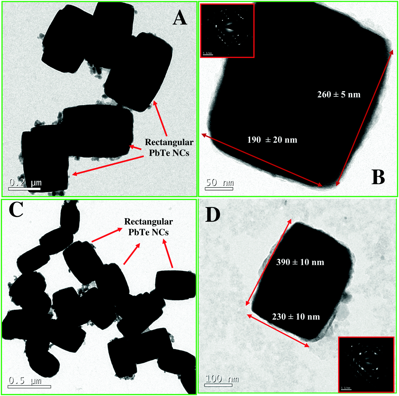 | ||
| Fig. 2 Transmission electron microscopy (TEM) images of the PbTe NCs. (A) and (B) show the low and high magnification TEM images of the smaller sized rectangular PbTe NCs, whereas (C) and (D) show the larger sized rectangular PbTe NCs. The insets in (B) and (D) show the corresponding selected area electron diffraction (SAED) patterns. | ||
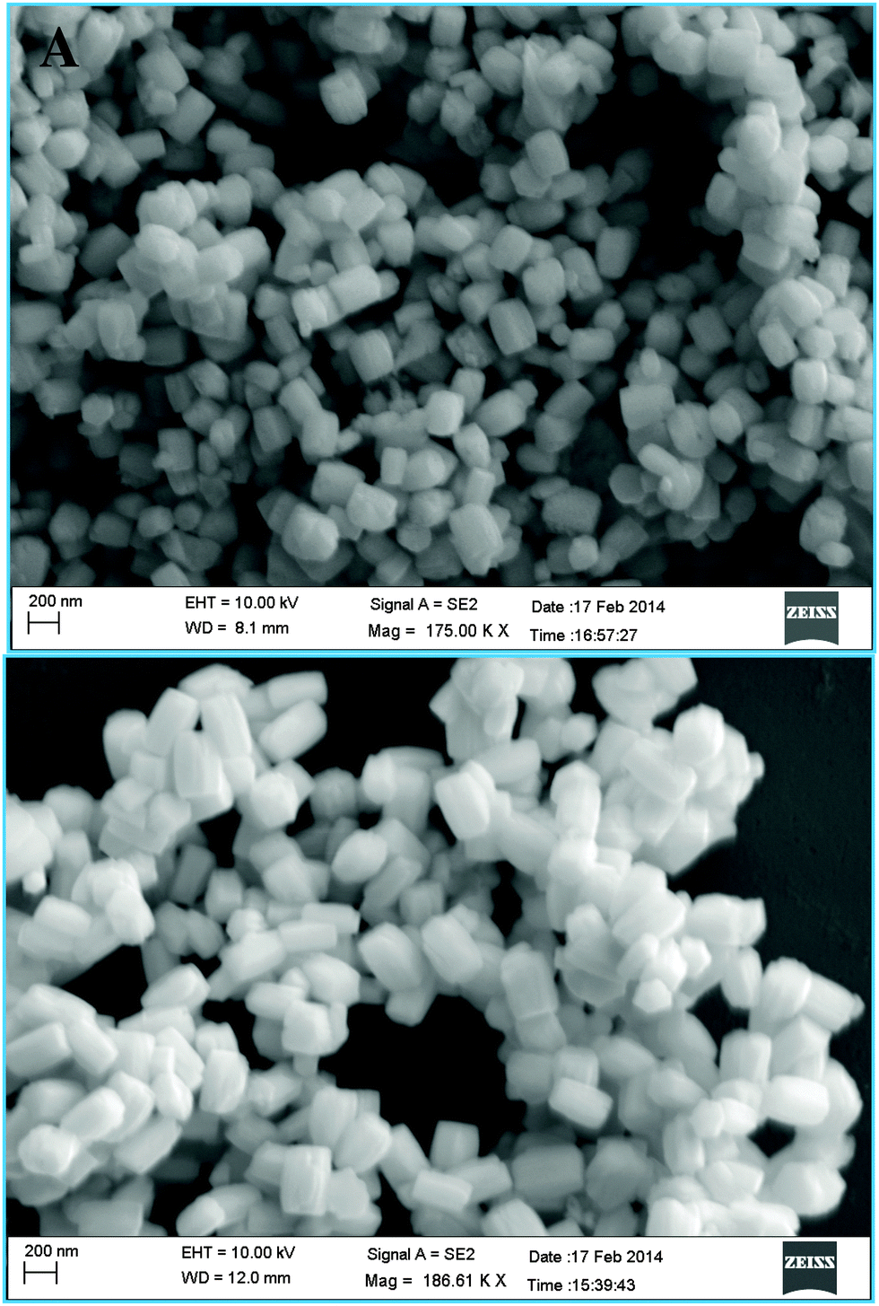 | ||
| Fig. 3 Field-emission scanning electron microscopy (FE-SEM) images of the rectangular PbTe NCs. (A) and (B) show the high magnification FE-SEM images for the smaller sized and larger sized PbTe NCs, respectively. | ||
Analysis of the PbTe NCs by X-ray diffraction (XRD)
The X-ray diffraction (XRD) patterns of the PbTe NCs are shown in Fig. 4. In Fig. 4, curves a and b indicate the XRD patterns of the small and large sized PbTe NCs, respectively. In both cases, we observed similar types of XRD patterns in terms of peaks but with intensity changes. The XRD curves are plotted in the 2θ range of 15–80 degrees. The diffraction peaks originate from the (111), (220), (200), (311), (222), (400), (331), (420) and (422) planes of the PbTe NCs within the experimental error (sys: cubic, S. G.: a = 6.459 Å). All the diffraction peaks are nicely matched with the joint committee for powder diffraction standard (JCPDS) file number 38-1435.16,19 Similar XRD patterns for cubic PbTe NCs have been reported before by Pan et al.16 and Hu et al.19 for their syntheses of PbTe nanomaterials of different morphologies. Zhu et al. have synthesized PbTe nanomaterials that have a face centered cubic (fcc) structure corresponding to JCPDS value 78-1905.28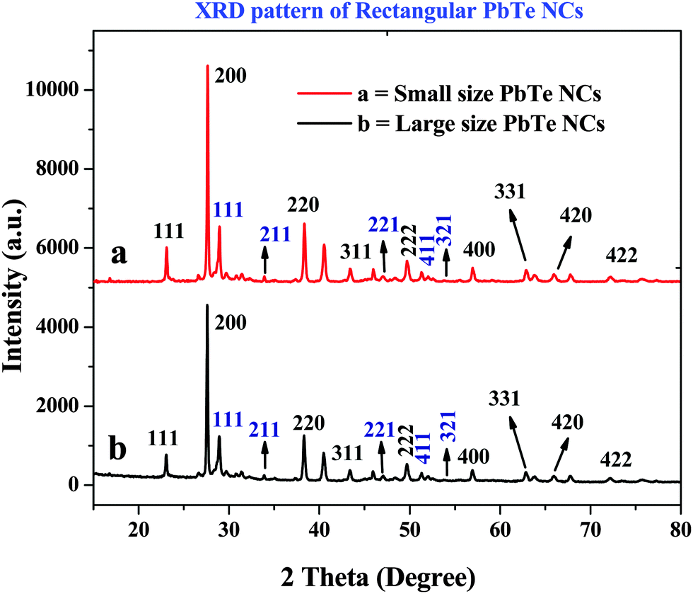 | ||
| Fig. 4 The X-ray diffraction (XRD) patterns of the rectangular PbTe NCs, where (a) portrays the small sized PbTe NCs and (b) the larger sized PbTe NCs. | ||
In our study, other than the original PbTe peaks, a few other low intensity peaks were also observed due to the presence of impurities, such as TeO2 having the JCPDS file no: 52-0795. In the XRD patterns in Fig. 4 the TeO2 crystal planes are indicated by a blue color. By comparing the features of the two XRD patterns, it can be seen that the relative intensity ratios of the strongest two peaks, which are the (200) and (220) peaks, for the as-synthesized PbTe products are 100![[thin space (1/6-em)]](https://www.rsc.org/images/entities/char_2009.gif) :27.42 (small size) and 100:26.73 (large size). The ratio of these two peaks for the standard PbTe powder in the JCPDS card is 100:75, suggesting that the synthesized PbTe products exhibited preferential crystallographic orientation of the (200) plane, when compared to the standard PbTe powder.19 The XRD patterns of the final materials after the spark plasma sintering (SPS) process have been recorded (not shown here) and the average crystal domain sizes of the two materials (before and after SPS) were compared. Before SPS, the average crystal domain sizes were 235 nm and 264 nm for the smaller and larger sized PbTe NCs, respectively. After SPS, the average crystal domain sizes were 295 nm and 320 nm for the smaller and larger sized PbTe NCs, respectively, according to the Scherrer equation. The increases in the crystal domain sizes were due to particle fusion, the particles compacting, gain growth and the increase in density while applying temperature and pressure during the SPS process. Hence, we confirmed that the synthesized PbTe NCs grew preferentially along the (200) plane, rather than the (220) plane, and that rectangular shapes were generated.
:27.42 (small size) and 100:26.73 (large size). The ratio of these two peaks for the standard PbTe powder in the JCPDS card is 100:75, suggesting that the synthesized PbTe products exhibited preferential crystallographic orientation of the (200) plane, when compared to the standard PbTe powder.19 The XRD patterns of the final materials after the spark plasma sintering (SPS) process have been recorded (not shown here) and the average crystal domain sizes of the two materials (before and after SPS) were compared. Before SPS, the average crystal domain sizes were 235 nm and 264 nm for the smaller and larger sized PbTe NCs, respectively. After SPS, the average crystal domain sizes were 295 nm and 320 nm for the smaller and larger sized PbTe NCs, respectively, according to the Scherrer equation. The increases in the crystal domain sizes were due to particle fusion, the particles compacting, gain growth and the increase in density while applying temperature and pressure during the SPS process. Hence, we confirmed that the synthesized PbTe NCs grew preferentially along the (200) plane, rather than the (220) plane, and that rectangular shapes were generated.
Analysis of the PbTe NCs by X-ray photoelectron spectroscopy (XPS)
Fig. 5 shows the X-ray photoelectron spectroscopy (XPS) images of the PbTe NCs. In Fig. 5, spectrum a represents the survey spectrum, while spectra b, c and d represent the high resolution spectra for Pb (4f), Te (3d) and O (1s), respectively. The survey spectrum in Fig. 5a consists of the characteristic peaks for Te (3d) at 581.2 eV, O (1s) at 530.2 eV, Pb (4d) at 419.45 eV, C (1s) at 285.2 eV, Pb (4f) at 146.2 eV and O (2s) at 26.6 eV. Fig. 5b shows the high resolution XPS scan for Pb 4f, which shows a doublet that originates from the spin–orbit coupling between the Pb 4f5/2 and Pb 4f7/2 peaks. The Pb 4f5/2 peak appears at a binding energy of 150.1 eV, while the Pb 4f7/2 peak appears at a binding energy of 145.3 eV. All the high resolution XPS spectra are deconvoluted and fitted with background spectra to clearly understand the exact peak positions. Fig. 5c shows the high resolution XPS spectrum for Te 3d, which also shows a doublet due to spin–orbit coupling between the Te 3d3/2 and Te 3d5/2 peaks. The Te 3d3/2 peak appears at a binding energy of 586.6 eV and the Te 3d5/2 peak appears at a binding energy of 576.2 eV. There are two other peaks that also appear at binding energies of 592.5 eV for Te 3d3/2 (TeO2) and 582.2 eV for Te 3d5/2 (TeO2).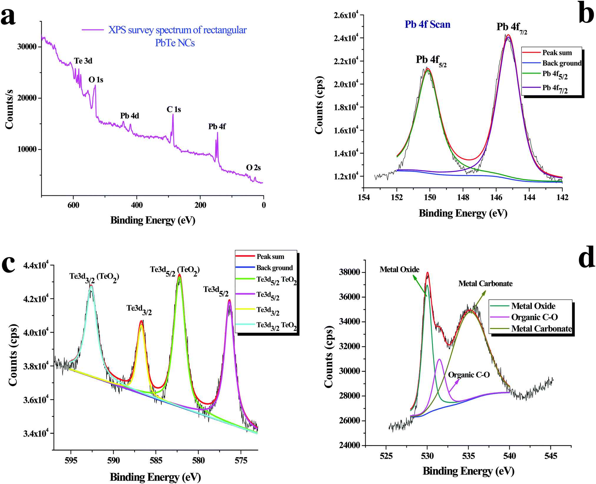 | ||
| Fig. 5 X-ray photoelectron spectroscopy (XPS) analysis of the PbTe NCs. (a) The survey spectrum, (b) the high resolution scan for Pb 4f, (c) the high resolution scan for Te 3d and (d) the high resolution scan for O 1s. | ||
Fig. 5d shows the high resolution spectrum of the O (1s) scan. Three different O peaks appear at binding energies of 530 eV for metal oxide, 531.5 eV for organic C–O and 535.2 eV for metal carbonate species. From the XPS analysis we concluded that within the PbTe nanomaterials, a small amount of TeO2 was present as an impurity, which was further supported by the XRD analysis (discussed before). Similar types of XPS spectra for PbTe have been reported earlier.33,34
Thermal analysis
The crystallization process of the as-prepared PbTe NCs was determined by thermogravimetric analysis (TGA) and differential thermal analysis (DTA) using a solid as-prepared PbTe sample of 2.66 mg. The sample was heated in the air up to 1000 °C at a heating rate 10 °C per minute. In Fig. 6, curve A is the TGA curve, while curve B is the DTA curve. From the TGA curve, we can see that the first weight loss took place near 109 °C and might have been due to the removal of moisture from the sample. The second weight loss took place at 327 °C due to the removal of excess organic moieties and excess surfactant molecules. There was another weight loss that took place near 503 °C, which was most probably due to the melting of excess Te metal powder in the sample. The final weight loss started at 763 °C and continued until the end, which might have been due to the melting of PbTe. Curve B shows the DTA curve, where there is an endothermic peak at 323 °C and a strong exothermic peak at 470 °C. This was probably due to the evaporation of excess CTAB or excess metal salt precursor. The final exotherm near 910 °C was due to melting of the synthesized PbTe NCs. Similar types of thermoelectric analyses have been reported earlier by others.21,35 From the thermal analysis we could see that after starting our reaction with 2.66 mg of sample and heating it up to 1000 °C, the amount of sample remaining was 0.733 mg. Hence the % weight loss during this process was 72.44%.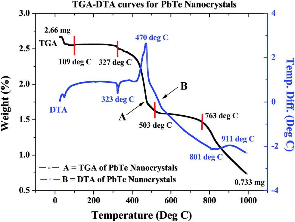 | ||
| Fig. 6 Thermal analysis of as-synthesized PbTe NCs, where curve A is the TGA curve and curve B is the DTA curve. | ||
FT-IR analysis
The FT-IR analyses of CTAB alone and the CTAB capped PbTe NCs are shown in Fig. 7. We have plotted both the CTAB and CTAB capped PbTe spectra together, which not only supports the presence of surfactant on the PbTe NC surfaces, but also indicates the nature of the interaction taking place among them. We checked that both of the rectangular PbTe NC morphologies gave similar types of FT-IR patterns. So here we plot the FT-IR spectrum of the large sized rectangular PbTe NCs. As the transmittance (%) value of the CTAB capped PbTe NCs was less than that of CTAB alone, the intensities of the peaks for CTAB–PbTe were lower compared to CTAB alone when they are plotted together. In the case of the CTAB sample, a small peak at 3470 cm−1 appeared, which was due to the –OH stretching originating from water molecules or the moisture adsorbed during the analysis. The broad peak at 3331 cm−1 was due to the well-known –N–H stretching vibration of pure CTAB molecules. Three strong and intense peaks appeared for the CTAB sample, at 3012 cm−1, 2918 cm−1 and 2847 cm−1, which were due to –C–H stretching and anti-stretching vibrations in the –CH2 group of the CTAB molecule. The 3331 cm−1 peak was not observed in the case of the CTAB bound PbTe sample, instead several low intensity peaks appeared in the 3536–3170 cm−1 region indicating the interaction of CTAB with the PbTe NCs. The –C–H stretching and bending peaks were also shifted in the case of the CTAB–PbTe sample, to 2926 cm−1 and 2846 cm−1, indicating the interaction of the surfactant with the PbTe NCs. In the case of the CTAB sample, a few other peaks appeared in the 1350–1800 cm−1 region at 1795 cm−1, 1628 cm−1, 1470 cm−1 and 1391 cm−1, which might have originated from –C–N stretching, the –CH2 scissoring mode of vibration and the –OH bending mode of water around the bound head group. All of these peaks were shifted or not visible in the case of the CTAB bound PbTe sample indicating the interaction among the components. In the case of the CTAB–PbTe sample, peaks appeared at 1739 cm−1 and 1397 cm−1. In the lower wavenumber region of 600–1000 cm−1, specifically at 955 cm−1, 906 cm−1 and 724 cm−1, peaks appeared due to the stretching vibration of the tertiary amine [RN(CH3)3+] and the –CH2 rocking, which was not at all visible in the case of the CTAB bound PbTe sample. Most of the peaks for CTAB and the CTAB capped PbTe NCs described above matched with earlier reports for CTAB capped metal and metal oxide nanostructures. Therefore, after analyzing the FT-IR data, it was clear that CTAB capped the PbTe NCs and stabilized them after the synthesis. Similar types of ligand stabilized PbTe NCs were reported earlier.21,36 The specific FT-IR peaks for CTAB (reported values),37 the FT-IR peaks for CTAB observed experimentally and the corresponding peak assignments are summarized in Table 2.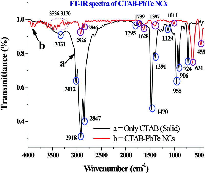 | ||
| Fig. 7 The Fourier-transform infrared (FT-IR) spectra of CTAB (curve a) and the CTAB bound PbTe NCs (curve b) in the wavenumber range of 400–4000 cm−1. | ||
| FT-IR band (cm−1) (experimentally observed) | FT-IR frequency range (cm−1) (reported value)37 | Absorbing bonds/vibration types |
|---|---|---|
| Reference: L. Huang, X. Chen and Q. Li, J. Mater. Chem., 2001, 11, 610. | ||
| 3331 | 3330 | –N–H stretching vibration |
| 3012 | 2959, 2870 | –CH3– anti-symmetric and symmetric stretching |
| 2918, 2847 | 2916, 2828 | –(CH2)– anti-symmetric and symmetric stretching |
| 1391 | 1376 | –CH3– symmetric deformation |
| 1129, 1253, 1284 | 1300–1000 (1041, 1151, 1265) | –(CH2)– out-plane swinging |
| 1034 | 1040 | Symmetric stretching vibration C–N bonds |
| 906, 955, 1470 | 908, 961, 1472 | Tertiary amine [RN(CH3)3+] |
| 724 | 720, 728 | –(CH2)– in-plane swinging |
Mechanism for the formation of rectangular PbTe NCs
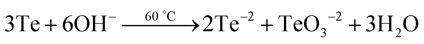
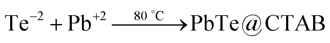
The rectangular PbTe NCs were formed by the reaction of Te metal powder with lead acetate solution in the presence of alkaline 2,7-DHN in CTAB micellar medium at low-temperature by heating at 80 °C. Two different sized but similarly rectangular morphologies were formed just by tuning the CTAB to metal salt precursor molar ratio. In our study, we conducted some control experiments to check the roles of all of the reagents used. We have seen that by keeping all of the reaction parameters fixed, but excluding CTAB, PbTe nanomaterials were formed but they had no specific size and shape and instead they were agglomerated after formation due to the absence of any specific stabilizing agent, as observed in the TEM analysis (image not shown here). On the other hand in the absence of alkaline 2,7-DHN, no reaction took place because there was no reducing agent in the solution for the reduction of the Te metal powder to generate Te2− ions. So, suitable concentrations of all the reagents were extremely necessary for the formation of specific shaped PbTe NCs. In our experiments, we checked the pH of the different solution mixtures during the synthesis. The pH of the Te metal powder aqueous solution was 5.38, the pH of Pb-acetate solution was 6.04, the pH of the alkaline 2,7-DHN solution was 13.20, the pH of the CTAB solution was 5.66 and the pH of a mixture of all the reagents, containing Te metal powder, Pb acetate, 2,7-DHN, NaOH and CTAB, was 11.65. Therefore, the overall reaction was taking place at basic pH. After the formation of the two different morphologies, we checked the pH values of aqueous dispersions of the PbTe NCs, which were 8.23 and 8.54 for the small and large sized rectangular PbTe NCs, respectively. In our studies, we did the experiments at a low temperature of ∼80 °C, so we believe that only ionic processes were taking place. Zhu et al.28 reported earlier that while the reaction takes place at a high-temperature in the presence of sodium borohydride as the reducing agent, both ionic and atomic processes take place during the formation of the PbTe NCs. In their reaction, they added all of the precursor at once and autoclaved at a higher temperature so that both atomic and ionic processes could contribute to the formation of the PbTe NCs. Moreover, Zhu et al. also reported that when the same reaction was carried out at low temperature (∼70 °C), they did not observe PbTe but they got PbO, tellurium oxide and even Te if the reaction time was increased to 24 hours.28 Hence we confirmed that in our present study at low temperature, the sequential addition of reagents could only contribute to ionic processes for the generation of the PbTe NCs. The possible chemical reactions that took place in our study are:

Therefore, in the proposed reaction, we believe that completely ionic processes were involved in generating PbTe and a small amount of tellurium oxide impurity was present in the final products, which was confirmed by XPS and XRD analyses. Zhu et al.28 mentioned that at lower temperature, if all the reagents are added at once, there is the possibility of partial lead reduction from Pb2+, which does not then completely react with Te and is easily oxidized to PbO during the filtering and drying processes. So, in our reaction the alkaline 2,7-DHN acted as a mild reducing agent, which converted TeO32− to Te2−, and CTAB acted as a shape-directing35 and capping agent for the generation of the PbTe NCs. It has already been reported previously that compounds having hydroxyl groups in their structure, like TX-100,38 ascorbic acid,39 2-naphthol35 and poly vinyl alcohol40 can act as reducing agents for the reduction of metal ions to metal NPs. Kundu et al. have also observed before that 2,7-DHN in alkaline conditions can reduce metal salts of Au,41 Ag,42 Pd43 and Os44 to their corresponding metal NPs. It is also reported that even deoxyribonucleic acid (DNA) with hydroxyl groups on its sugar analogue can be used to reduce metal ions to generate DNA-templated metal NPs.45–47 So in our present process, once the Te metal has been reduced by alkaline 2,7-DHN to form Te2− and the lead salt has been added to the reaction mixture, they react with each other immediately and generate PbTe nuclei. Once the PbTe nuclei are formed, they grow indiscriminately accumulating more Te2− ions and creating a void space surrounding the fully grown particles. The PbTe nuclei are formed close to the interface and favor crystallization in a preferential direction. With increasing time, the formation of the PbTe nuclei reduces and finally a slow crystallization process takes place and all the PbTe nuclei are converted to PbTe particles with rectangular shapes. As the solution already contains the CTAB surfactant, micelles get adsorbed onto particular facets of the PbTe crystals and direct the 3D growth of the evolved NPs to give the desired rectangular shape. It is reported in the literature that the formation of a specific shape depends upon two key factors; one is the faceting tendency of the stabilizing agent and the other is the growth kinetics, that is the rate at which PbTe(0) is supplied to the different crystallographic planes.48 The CTAB surfactant adsorbs onto the surfaces of these crystalline particles and slows down the growth rate of the different crystal facets. We observed that for both of the CTAB concentrations, rectangular PbTe particles were formed although the sizes of the particles were smaller at the higher CTAB concentration, while the sizes of the particles were larger at the low CTAB concentration. It is reported that when the growth rates of the (111) and (100) planes are almost the same, nanocubes are mostly formed but once the growth rate is slightly more or less in any one of the planes, a rectangular morphology can be formed. Hence in our case we confirmed that the growth rates of the two facets were not completely equal resulting in the rectangular shaped particles. Xia's group have also reported before that when the growth rate is predominant in either the (100) or (111) directions, anisotropic shapes like tetra-pods and octa-pods are mostly formed.49,50 Murphy et al.18 have also reported that high surface energy {111} face growth in the 〈111〉 direction is faster relative to that of the large surface energy {100} face growth in the 〈100〉 direction, which favors the growth of the {100} face more and generates cubic morphology. In our case, at a high CTAB concentration, the growth rate in both crystal faces was somehow restricted and resulted in the smaller sized rectangular PbTe NCs, while at the comparatively lower CTAB concentration, the growth in both faces was greater and resulted in the large sized rectangular PbTe NCs. The evolved rectangular PbTe NCs were well separated from each other due to the fact that the CTAB surfactant was adsorbed onto the particle surfaces, which may have formed capping shells, generating regular inter-particle spacing and preventing the rectangles from undergoing random agglomeration.51 At this point, the exact bonding geometry and the nature of the selective interaction between the crystallographic planes are still not fully clear and further study is necessary, which will be conducted in near future. Next, we took the two different morphologies of PbTe NC and we studied their applications in a thermoelectric power generation study, as discussed below.
Thermoelectric applications of rectangular PbTe NCs
In our present study, we synthesized two different sizes of rectangular shaped PbTe NCs using a wet-chemical route. The wet-chemical route easily produced material with nanoscale dimensions that could be used to reduce the thermal component via phonon scattering and by decoupling electrical and thermal conductivities.52 Even though there are a few reports available on the synthesis of PbTe nanomaterials, we focused here on the effect of nanomaterial size on TE behaviour. The synthesized PbTe NCs were analyzed to determine their thermal diffusivity, electrical conductivity Seebeck coefficient and finally concluding with their ZT values. Theoretical and experimental reports on different TE materials say that high phonon anharmonicity is the most important consideration when designing highly TE materials.53–58In the present analysis, we compared the TE properties of two differently sized rectangular shaped PbTe NCs. For the TE measurements, all of the samples were subjected to SPS consolidation at 300 °C under 400 MPa pressure for 5 minutes and the relative densities of the samples were about 98.5%. Fig. 8A shows the electrical conductivity measurements of the small (a) and large (b) sized rectangular PbTe NCs with respect to temperature. The small sized PbTe NCs showed typical semiconductor behavior in the temperature range of 300–380 K because increasing the temperature also increases the electrical conductivity. After 380 K, the sample showed metallic behaviour because with increasing temperature, the conductivity was decreasing. For the small sized rectangular NCs in the region of 380 K, a structural phase transition may have occurred, as was also observed in an earlier report and was shown to occur at around 410 K for the Ag2Te alloy structure, which changed from β-Ag2Te to α-Ag2Te due to a large decrease in carrier concentration.59 However, the small sized rectangular PbTe NCs had a noticeable flattening, which started at 400 K and indicated degenerate semiconductor behavior at high temperatures due to the decrease in electron–electron and electron–phonon scattering conductivities. Finally, at a temperature of 480 K, the small sized rectangular PbTe NCs showed high electrical conductivity behavior. The large sized rectangular PbTe NCs initially showed metallic behaviour but after a certain temperature, this changed to semiconducting in nature. At high temperatures, as the carrier concentration increased, the Seebeck values decreased as shown in Fig. 8B. As we can note from the Seebeck coefficient versus temperature graphs, the small (a) and large (b) sized samples showed degenerate (highly doped) behavior, which means that as the temperature increased, the Seebeck values were also increased.
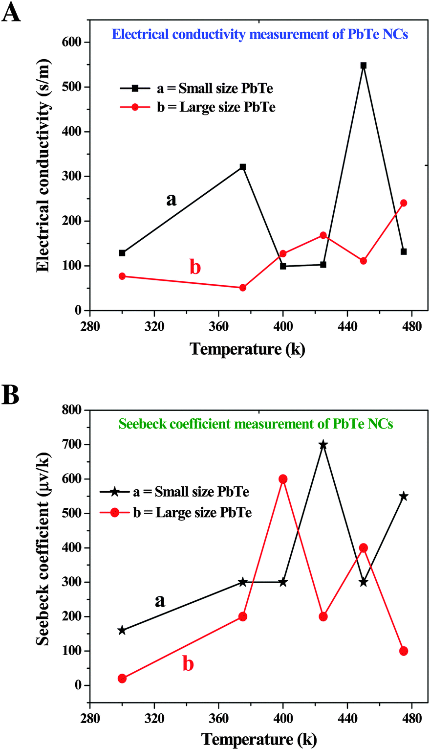 | ||
| Fig. 8 Thermoelectric behavior of the synthesized small (a) and large (b) sized rectangular PbTe NCs. (A) Electrical conductivity measurements and (B) Seebeck coefficient variation with change in temperature. | ||
Both of the samples showed typical intrinsic semiconductor behavior results through the decrease of their Seebeck coefficients at high temperatures. The Seebeck coefficients also depend on the electrical conductivities of the materials. From the curves, we can see that sudden increases and decreases took place in the range of ∼370–460 K in both samples, which may be due to structural phase transitions, as observed in an earlier report.59 The high Seebeck coefficient values obtained at high temperature are due to the well-known contribution of the two valence bands present in PbTe.57
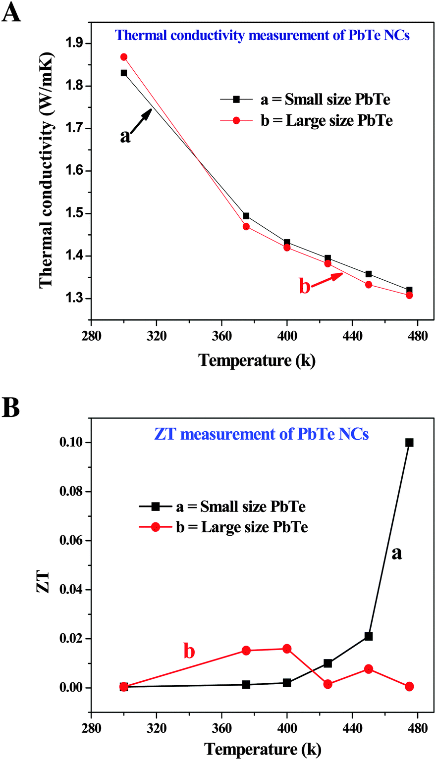
The changes in the thermal conductivity values as a function of temperature are shown in Fig. 9A. The thermal behavior of both the small (a) and large (b) sized rectangular PbTe NCs gradually decreased with increasing temperature. All of the κ values decreased for both sizes of PbTe system indicating Umklapp scattering (phonon–phonon scattering) at high temperatures. At a temperature of 475 K, the small and large sized PbTe NCs showed nearly the same thermal conductivity of around 1.3 W m−1 K−1. In the case of nanomaterials, when their grain sizes are smaller than 5 μm, then the lattice thermal conductivity is reduced by ca. 28% compared to the bulk material. Particles with sizes in the range of 30–200 nm and crystallites of 5–15 nm in size show boundary scattering of phonons, thereby reducing their thermal conductivity by ca. 46%, which leads to reduced electron mobility and enhanced ZT values.60 Generally, a low lattice thermal conductivity is obtained when the phonons are scattered by impurities present in a sample.61
 | ||
| Fig. 9 Thermoelectric behavior of the synthesized small (a) and large (b) sized rectangular PbTe NCs. (A) Thermal conductivity measurements and (B) figure of merit (ZT) values with change in temperature. | ||
Fig. 9B shows the temperature dependent ZT values of the two different sized PbTe NCs. The small sized (a) rectangular PbTe NCs achieved a maximum ZT value of ∼0.1 at 475 K, while the larger sized (b) NCs showed a maximum ZT value of ∼0.015 at 400 K. We compared the values at different temperatures because the larger sized NCs gave a much lower ZT value at 475 K. The ZT value of the small sized PbTe NCs showed a linear increment with increasing temperature. From the electrical conductivity measurements, it has already been observed that the small sized rectangular PbTe NCs showed a higher electrical conductivity than the large sized PbTe NCs (Fig. 7a). The Seebeck coefficient value reduced at ∼440 K, indicating the high conductivity behaviour of the sample. Low dimensional nanostructured materials show phonon-glass/electron-crystal (PGEC) behavior that leads to a high TE performance.52,62,63 In summary, all of the above analyses indicate that the small sized PbTe NCs exhibit a higher power factor value, as well as a lower thermal conductivity value, compared to the large sized PbTe NCs, which in-turn results in a higher ZT value in comparison to the large sized rectangular PbTe NCs.
Conclusion
In conclusion, we report for the first time, a low-temperature route for the successful generation of rectangular PbTe nanocrystals within a short time under heating at 80 °C. PbTe nanocrystals were formed by the reaction of Te metal powder with Pb-acetate salt in the presence of alkaline 2,7-dihydroxy naphthalene solution and in a cetyl trimethyl ammonium bromide micellar medium. Two different sized rectangular PbTe nanocrystals were formed just by tuning the cetyl trimethyl ammonium bromide to metal salt precursor molar ratio and by controlling the other reaction parameters. The average size of the small sized rectangular nanocrystals was 260 ± 5 nm (longer side) by 190 ± 20 nm (shorter side) and the large sized rectangular nanocrystals were 390 ± 20 nm (longer side) by 230 ± 10 nm (shorter side). The optical properties, thermal stabilities and electronic properties of the PbTe nanocrystals were studied in detail utilizing various instrumental techniques. The growth mechanism for the formation of the rectangular PbTe nanocrystals has been elaborated in detail. Finally, both of the morphologies have been assessed for their application as thermoelectric materials. It was observed that both sizes of rectangular PbTe nanocrystals could be used as thermoelectric materials and among the two morphologies, the smaller sized rectangular PbTe nanocrystals gave a better thermoelectric figure of merit value compared to the larger size at 475 K. The achievement of a higher efficiency in the case of smaller sized rectangular PbTe nanocrystals was due to their higher power factor value and low thermal conductivity properties. In the future, we will try to improve the observed efficiency to a great extent by controlling the nanomaterial morphology through the introduction of impurities or dopants within the synthesized material.Acknowledgements
S. Kundu wishes to acknowledge Dr Vijayamohanan K. Pillai, Director, and Dr M. Jayachandran, HOD, of the ECMS division, CSIR-CECRI for their continuous support and encouragement. U. Nithiyanantham wishes to thank CSIR-CECRI for a research-intern fellowship. Critical discussions with Prof. H. Liang at TAMU and Ede Sivasankara Rao and S. Anantharaj at CSIR-CECRI are greatly acknowledged. The institute start up funding (Project number IHP 0067, DU No 5, old number OLP-0067), support from the Central Instrumental Facility (CIF) and help from Mr A. Rathishkumar (TEM in-charge), Mr J. Kennedy (XPS in-charge), Mr V. Prabu (FE-SEM in-charge, CIF), CSIR-CECRI, Karaikudi are greatly appreciated.References
- M. Fardy, A. I. Hochbaum, J. Goldberger, M. M. Zhang and P. Yang, Adv. Mater., 2007, 19, 3047 CrossRef CAS.
- H. J. Goldsmid, in CRC Handbook of Thermoelectrics, ed. D. M. Rowe, Boca Raton, FL, CRC Press, 2006 Search PubMed.
- M. Baleva and E. Mateeva, Phys. Rev. B: Condens. Matter Mater. Phys., 1994, 50, 8893 CrossRef CAS.
- G. L. Benneu, in CRC Handbook of Thermoelectrics, ed. D. M. Rowe, CRC, New York, 1995, p. 515 Search PubMed.
- L. D. Hicks and M. S. Dresselhaus, Phys. Rev. B: Condens. Matter Mater. Phys., 1993, 47, 12727 CrossRef CAS.
- F. Gao, Q. Lu, X. Liu, Y. Yan and D. Zhao, Nano Lett., 2001, 1, 743 CrossRef CAS.
- K.-S. Cho, D. V. Talapin, W. Gaschler and C. B. Murray, J. Am. Chem. Soc., 2005, 127, 7140 CrossRef CAS PubMed.
- K. L. Hull, J. W. Grebinski, T. H. Kosel and M. Kuno, Chem. Mater., 2005, 17, 4416 CrossRef CAS.
- E. Lifshitz, M. Bashouti, M. V. Kloper, A. Kigel, M. S. Eisen and S. Berger, Nano Lett., 2003, 3, 857 CrossRef CAS.
- C. Zhang, Z. Kang, E. Shen, E. Wang, L. Gao, F. Luo, C. Tian, C. Wang, Y. Lan, J. Li and X. Cao, J. Phys. Chem. B, 2006, 110, 184 CrossRef CAS PubMed.
- L. Zhang, J. C. Yu, M. Mo, L. Wu, K. W. Kwong and Q. Li, Small, 2005, 1, 349 CrossRef CAS PubMed.
- J.-P. Ge, J. Wang, H.-X. Zhang, X. Wang, Q. Peng and Y.-D. Li, Chem. – Eur. J., 2005, 11, 1889 CrossRef CAS PubMed.
- H. Q. Liu, F. X. Hao, J. Guo, Y. J. Gu, Q. K. He and H. Z. Cui, Proc. 2012 Int. Conf. on 3M-NANO, Xi'an, China, August–September 2012, IEEE, 382–384.
- H. Li, K. F. Cai, J. L. Yin, H. F. Wang, X. L. Li, Y. Y. Wang and C. W. J. Zhou, J. Nanosci. Nanotechnol., 2010, 10, 5831 CrossRef CAS PubMed.
- L. Ao, L. J. Wang and W. Z. Wang, Micro Nano Lett., 2012, 7, 621 Search PubMed.
- Y. Pan, H. Bai, L. Pan, Y. Li, M. C. Tamargo, M. Soheld and J. R. Lombardiab, J. Mater. Chem., 2012, 22, 23593 RSC.
- T. Mokari, M. Zhang and P. Yang, J. Am. Chem. Soc., 2007, 129, 9864 CrossRef CAS PubMed.
- J. E. Murphy, M. C. Beard, A. G. Norman, S. P. Ahrenkiel, J. C. Johnson, P. Yu, O. IMicic, R. J. Ellingson and A. J. Nozik, J. Am. Chem. Soc., 2006, 128, 3241 CrossRef CAS PubMed.
- J. Hu, Z. Chen, H. Jiang, Y. Sun, Y. Bandoc and D. Golberg, J. Mater. Chem., 2009, 19, 3063 RSC.
- S. Chen, K. F. Cai and F. Y. Li, Mater. Res. Innovations, 2014, 18, S4–S97 CAS.
- C. Papageorgiou, J. Giapintzakis and T. Kyratsi, J. Electron. Mater., 2013, 42, 1911 CrossRef CAS.
- J.-F. Li, W.-S. Liu, L.-D. Zhao and M. Zhou, NPG Asia Mater., 2010, 2, 152 CrossRef.
- G. A. Tai, B. Zhou and W. L. Guo, J. Phys. Chem. C, 2008, 112, 11314 CAS.
- N. Zhou, G. Chen, X. Yang and X. Zhang, J. Phys. Chem. Solids, 2012, 73, 280 CrossRef CAS.
- T. J. Zhu, X. Chen, X. Y. Meng, X. B. Zhao and J. He, Cryst. Growth Des., 2010, 10, 3727 CAS.
- H. Cao, Q. Gong, X. Qian, H. Wang, J. Zai and Z. Zhu, Cryst. Growth Des., 2007, 7, 425 CAS.
- Q. Li, Y. Ding, M. Shao, J. Wu, G. Yu and Y. Qian, Mater. Res. Bull., 2003, 38, 539 CrossRef CAS.
- T. J. Zhu, Y. Q. Liu and X. B. Zhao, Mater. Res. Bull., 2008, 43, 2850 CrossRef CAS.
- H. Du, C. Chen, R. Krishan, T. D. Krauss, J. M. Harbold, F. W. Wise, M. G. Thomas and J. Silcox, Nano Lett., 2002, 2, 1321 CrossRef CAS.
- F. Soofivand, F. Mohandes and M. Salavati-Niasari, Micro Nano Lett., 2012, 7, 283 Search PubMed.
- D. Zhang, H. Fu, L. Shi, C. Pan, Q. Li, Y. Chu and W. Yu, Inorg. Chem., 2007, 46, 2446 CrossRef CAS PubMed.
- F. Mohandes and M. Salavati-Niasari, Ultrason. Sonochem., 2013, 20, 354 CrossRef CAS PubMed.
- R. Jin, G. Chen, J. Pei, J. Sun and Q. Wang, CrystEngComm, 2012, 14, 4461 RSC.
- W. Zhao, P. Y. Ge, J. J. Xu and H. Y. Chen, Langmuir, 2007, 23, 8597 CrossRef CAS PubMed.
- S. Kundu, S. Panigrahi, A. Pal, S. Basu, S. Praharaj, S. K. Ghosh and T. Pal, Nanotechnology, 2007, 18, 75712 CrossRef PubMed.
- S. AhMadian-Fard-Fini, M. Salavati-Niasari and F. Mohandes, Bull. Mater. Sci., 2014, 37, 753 CrossRef CAS.
- L. Huang, X. Chen and Q. Li, J. Mater. Chem., 2001, 11, 610 RSC.
- S. Kundu, K. Wang and H. Liang, J. Phys. Chem. C, 2009, 113, 134 CAS.
- A. Pal and T. Pal, J. Raman Spectrosc., 1999, 30, 199 CrossRef CAS.
- S. Kundu, D. Huitink, K. Wang and H. Liang, J. Colloid Interface Sci., 2010, 344, 334 CrossRef CAS PubMed.
- S. Kundu, L. Peng and H. Liang, Inorg. Chem., 2008, 47, 6344 CrossRef CAS PubMed.
- S. Kundu, K. Wang and H. Liang, J. Phys. Chem. C, 2009, 113, 134 CAS.
- S. Kundu, K. Wang, S. Lau and H. Liang, J. Nanopart. Res., 2010, 12, 2799 CrossRef CAS.
- S. R. Ede, U. Nithiyanantham and S. Kundu, Phys. Chem. Chem. Phys., 2014, 16, 22723 RSC.
- S. Kundu, Phys. Chem. Chem. Phys., 2013, 15, 14107 RSC.
- D. Majumdar, A. Singha, P. K. Mondal and S. Kundu, ACS Appl. Mater. Interfaces, 2013, 5, 7798 CAS.
- U. Nithiyanantham, S. R. Ede and S. Kundu, J. Mater. Chem. C, 2014, 2, 3782 RSC.
- J. M. Petroski, Z. L. Wang, T. C. Green and M. A. El-Sayed, J. Phys. Chem. B, 1998, 102, 3316 CrossRef CAS.
- T. Herricks, J. Chen and Y. Xia, Nano Lett., 2004, 4, 2367 CrossRef CAS.
- B. Lim, X. Lu, M. Jiang, P. H. C. Camargo, E. C. Cho, E. P. Lee and Y. Xia, Nano Lett., 2008, 8, 4043 CrossRef CAS PubMed.
- C. B. Murray, C. R. Kagan and M. G. Bawendi, Annu. Rev. Mater. Sci., 2000, 30, 545 CrossRef CAS.
- C. Kim, D. H. Kim, H. Kim and J. S. Chung, ACS Appl. Mater. Interfaces, 2012, 4, 2949 CAS.
- H. Zhang and D. V. Talapin, Angew. Chem., Int. Ed., 2014, 53, 9126 CrossRef CAS PubMed.
- H. Liu, X. Shi, F. Xu, L. Zhang, W. Zhang, L. Chen, Q. Li, C. Uher, T. Day and G. J. Snyder, Nat. Mater., 2012, 11, 422 CrossRef CAS PubMed.
- C. Wood, Rep. Prog. Phys., 1988, 51, 459 CrossRef CAS.
- G. H. Dong, Y. J. Zhu and L.-D. Chen, J. Mater. Chem., 2010, 20, 1976 RSC.
- K. Biswas, J. He, I. D. Blum, C. I. Wu, T. P. Hogan, D. N. Seidman, V. P. Dravid and M. G. Kanatzidis, Nature, 2012, 489, 414 CrossRef CAS PubMed.
- L. D. Zhao, S. H. Lo, Y. Zhang, H. Sun, G. Tan, C. Uher, C. Wolverton, V. P. Dravid and M. G. Kanatzidis, Nature, 2014, 508, 373 CrossRef CAS PubMed.
- J. Pei, G. Chen, D. Jia, Y. Yu, J. Sun, H. Xu and Z. Qiu, New J. Chem., 2014, 38, 59 RSC.
- P. Vaqueiro and A. V. Powell, J. Mater. Chem., 2010, 20, 9577 RSC.
- P. Zhu, Y. Imai, Y. Isoda, Y. Shinohara, X. Jia and G. Zou, Mater. Trans., 2005, 46, 1810 CrossRef CAS.
- K. Kurosaki, T. Matsuda, M. Uno, S. Kobayashi and S. J. Yamanaka, J. Alloys Compd., 2001, 319, 271 CrossRef CAS.
- S. Paschen, V. Pacheco, A. Bentien, A. Sanchez, W. C. Cabrera, M. Baenitz, B. B. Iversen, Y. Grin and F. Steglich, Physica B, 2003, 328, 39 CrossRef CAS.
| This journal is © The Royal Society of Chemistry and the Centre National de la Recherche Scientifique 2016 |