
Highly sensitive and uniform surface-enhanced Raman spectroscopy from grating-integrated plasmonic nanograss†
Yang
Shen
ab,
Xizhe
Cheng
a,
Guozhen
Li
a,
Qiangzhong
Zhu
a,
Zhenguo
Chi
b,
Jianfang
Wang
*c and
Chongjun
Jin
*a
aState Key Laboratory of Optoelectronic Materials and Technologies, School of Materials Science and Engineering, Sun Yat-sen University, Guangzhou 510275, China. E-mail: jinchjun@mail.sysu.edu.cn
bSchool of Chemistry and Chemical Engineering, Sun Yat-sen University, Guangzhou 510275, China
cDepartment of Physics, The Chinese University of Hong Kong, Shatin, Hong Kong SAR, China. E-mail: jfwang@phy.cuhk.edu.hk
First published on 4th May 2016
Abstract
Surface-enhanced Raman scattering (SERS) spectroscopy has found a wide range of applications in biomedicine, food safety and environmental monitoring. However, to date, it is difficult for most SERS substrates to provide an extremely sensitive and highly uniform Raman response simultaneously. Here, we developed a sensitive and uniform SERS sensing strategy based on grating-integrated gold nanograsses (GIGNs), which can amplify the SERS signal up to 10-fold compared to the nanograss without grating (namely on the flat substrate) experimentally. Numerical simulation results show that such an improvement of SERS sensitivity arises from the enhanced hotspots relying on the strong coupling between the localized surface plasmon resonances of individual stripe-regulated gold nanorod assemblies and Wood’s anomalies in air and dielectric grating. Importantly, these hotspots on the substrate can be flexibly tailored by adjusting the height and periodicity of the loaded grating. The SERS performances of the GIGNs have further been successfully demonstrated with the label-free detection of adenine and cytosine (DNA bases) molecules at the nanomolar level. Moreover, the GIGNs also presented the uniform spot-to-spot and sample-to-sample SERS signals of the analyte molecules (relative standard deviations down to ∼11% and 13%, respectively). These advantages suggest that our GIGN substrates are of great potential for SERS-related sensing.
Conceptual insightsThis work introduces a method in the design and fabrication of a low-cost SERS-active substrate with highly sensitive and uniform Raman response simultaneously. Very different from the nanoparticle assembly in a flat substrate, our non-planar counterpart, called grating-integrated gold nanograss (GIGN), boosts its SERS performance relying on the strong couplings between the localized surface plasmon resonances (LSPRs) from the gold nanograsses and Wood’s anomalies of the grating. Through controlling the height and periodicity of the grating, one can tailor the resonant modes as well as the associate local hotspots distribution, and finally manipulate the SERS response of the GIGNs. Moreover, the local hotspot distributions that are dominated by the grating effect will minimize the degradation in signal uniformity caused by structural inhomogeneity. The highly sensitive and uniform SERS response, together with the compatibility with low-cost fabrication methods (such as self-assembly of metal nanoparticles and oblique angle deposition), paves the way for the development of practical SERS-related applications. |
Surface-enhanced Raman scattering (SERS) allows for the identification of single or few molecules located at an electromagnetic “hotspot” very efficiently through their unique vibrational fingerprints.1–3 An ideal SERS-active substrate for sensing and imaging applications should possess a giant signal enhancement, a highly uniform and reproducible response, and an easy fabrication method simultaneously.4 A drastic local electromagnetic (EM) field enhancement acting on the molecules, driven by the localized surface plasmon resonances (LSPRs) from the metallic nanostructures, is widely considered to be a main origin for the amplification of the cross-section of this inelastic scattering.5 In this regard, great efforts have been devoted to maximizing local fields within metallic nanostructures.6–36 An effective approach is to use the nanoparticles and nanostructures that contain sharp edges,6,7 few-nanometer gaps8–19 and conductive nanobridges.4,20 For example, some novel nanostructures such as “flower-like” nanoparticles,21 hollow nanourchins,6 nanostar dimers,11 nanobridged particles4 and nanosnowman structures20 have been synthesized chemically or fabricated lithographically for SERS purpose. Another challenge is how to obtain a highly uniform and reproducible SERS signal, i.e. generation of a narrow distribution of high enhancement factor values, which is indispensable for reliable quantitative detection in practice.4,37,38 Unfortunately, chemically prepared hotspots in solutions are generally random and uncontrollable owing to their variability in particle distance, surface, size and shape.4 In contrast, the high-resolution lithographic techniques enable a precise control of particle shape, size and gap distance, and thus higher probe stability, but it is costly and time-consuming.9 Furthermore, limited by the nature of the fabrication method, the lithographically prepared nanostructures hardly provide a dense hotspots distribution. This may hamper sensing single/few molecules at ultralow concentrations even if the hotspots are precisely prefabricated, because the molecules are probably located outside the hotspots regions. To date, the most efficient solution to the aforementioned problems is assembling the nanoparticles into close-packed arrays at solid substrates6,7,22–24 and liquid/liquid or liquid/air interfaces.25–28 Through the production of multiple hotspots in a large area, this strategy has demonstrated an extreme SERS sensitivity that is enough even for probing a single molecule.28 However, in these cases, the densities of these hotspots and interaction between the nanoparticles are ultimately limited to a two-dimensional plane.29 Recently, new types of non-planar SERS substrates, including three-dimensional hotspot matrix29 and nanoparticle assemblies on the structured substrates (such as metallic grating,30 nanocavity arrays31 and non-metallic nanosphere arrays32), have been used for SERS and have demonstrated a further improvement in the SERS signal.
Quasi-randomly arranged gold nanorod assemblies, achieved in glass35,39–41 or flexible substrates42,43 using oblique angle deposition (OAD), have shown excellent SERS performances. Here we demonstrate a highly sensitive and uniform SERS spectroscopy using a novel structure that consists of such a quasi-randomly arranged gold nanorod assembly, the so-called nanograss, supported by a dielectric grating. In this grating-integrated gold nanograss (GIGN), an enhancement factor of ∼10 in SERS intensity for R6G was obtained, which is higher than that of the non-grating-integrated gold nanograss (NGIGN, namely a gold nanograss on a flat substrate). The numerical simulations show that the boost of SERS sensitivity is caused by the two additional field enhancement channels relying on the lateral and vertical coupling between the grating-regulated gold nanorod assemblies, respectively. In addition, the narrow distributions of spot-to-spot and sample-to-sample SERS signals of the R6G with the relative standard deviations down to ∼11% and 13% are demonstrated, respectively. Finally, biosensing based on the GIGN is demonstrated with its detection limits down to 10 nM and 100 nM for detecting adenine and cytosine, respectively.
Fig. 1a depicts the fabrication scheme used to generate GIGN over a large area. We employed two-beam interference lithography to pattern a grating of photoresist stripes in advance, followed by molding of its complementary structure with PDMS (polydimethylsiloxane) elastomer.44 Finally, a glancing electron beam evaporation of 5 nm nickel and 120 nm gold along the direction of the grooves was applied to form the oriented gold nanograss on the groove-embedded PDMS substrate, namely GIGN. Fig. 1b and c show the cross-sectional scanning electron microscopy (SEM) images of a grating of photoresist stripes on a quartz substrate and its inverse version made of PDMS elastomer, respectively. Fig. 1d highlights a typical sample size (up to 3 cm2) that can be readily reproduced on the flexible PDMS substrates. Fig. 1e and f show the SEM images of a GIGN and a NGIGN, which are taken from the regions indicated by the red and blue squares in Fig. 1d, respectively. As shown in Fig. 1d, the grating-integrated area exhibits a strong diffraction of light. In contrast, it shows no diffraction from the unstructured area on the edge of the sample. The lattice constant of the grating a is 450 nm, and the height, top and bottom widths of the stripes (h, w1 and w2) are 150, 250 and 320 nm, respectively. The length l and diameter d of the gold nanorods are 120 ± 15 and 25 ± 5 nm respectively and their tilting angle θ with respect to the surface plane is 15°. The average separations between the nanorods in x and y axes, sx and sy, are 37 and 80 nm, respectively. The sizes of gold nanorods are obtained from the top-view and cross-sectional SEM images of the GIGNs (Fig. S1, ESI†). It should be noted that the gold nanograsses and the underneath thin gold film with a thickness of ∼30 nm were formed simultaneously due to the nature of glancing gold deposition. That is to say, the base of each tilting nanorod sticks on the surface of the thin gold film. In addition, the bottom of each PDMS stripe is larger than the top, leading to a cover of the gold nanorods on the side walls of the PDMS stripe during electron beam evaporation of gold. The entire structure looks like a gold nanograss grown on a groove-embedded PDMS substrate. The detailed fabrication procedure can be found in the ESI.†
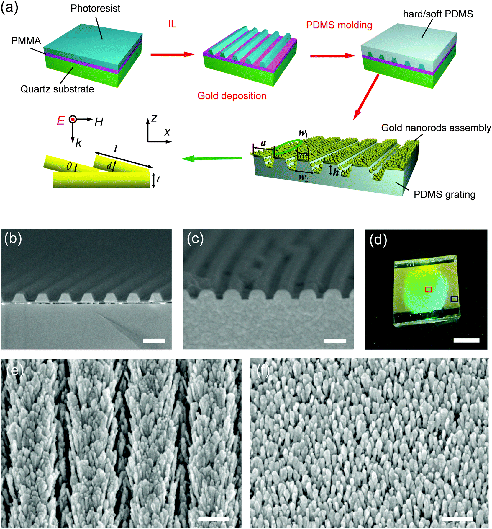 | ||
| Fig. 1 GIGNs. (a) Schematic showing the fabrication procedure of GIGNs. IL stands for interference lithography. PMMA and PDMS refer to poly(methyl methacrylate) and polydimethylsiloxane, respectively. (b) Cross-sectional SEM image of a photoresist grating (lattice constant a = 450 nm and stripe height h = 150 nm) formed by interference lithography. (c) Cross-sectional SEM image of a PDMS grating (a = 450 nm, h = 150 nm, w1 = 250 nm, w2 = 320 nm) after molding. (d) Optical photograph of a GIGN on a flexible PDMS substrate with the periodic grooves. (e and f) Top-view SEM images of a GIGN and a NGIGN, corresponding to the regions indicated by the red and blue squares on the same sample in (d), respectively. The thickness t of the bottom gold layer is 30 nm. The length l and diameter d of gold nanorods are 120 ± 15 and 25 ± 5 nm respectively and their tilting angle θ with respect to the surface plane is 15°. The average separations sx and sy between the nanorods in x and y axes are 37 and 80 nm, respectively. (b and c) Scale bar: 400 nm. (d) Scale bar: 1 cm. (e and f) Scale bar: 200 nm. | ||
To predict the optical properties of the GIGNs, we calculated the absorption spectra and corresponding electric field intensity distributions using the finite-difference time-domain (FDTD) method. It should be noted that absorption is defined as A = 1 − R − T in this work, and we obtained the absorption spectra through simulation or measurement of the corresponding reflection and transmission spectra, respectively. Here, to explore the role of the grating acting on the optical properties of the GIGNs, we simplified the structure by replacing the randomly but parallel arranged nanorod array with a regular one. This simplification is based on the fact that the separations between the nanorods are much smaller than the wavelength of light used in the experiments, so only average values of nanorod assembly parameters are important, and the deviations of the separations between the nanorods only have limited influence on the overall optical properties of an assembly of Au nanorods45–47 (comparison of the simulated optical properties on uniform and random GIGNs can be seen in Fig. S2, ESI†). Fig. 2 presents a side-by-side comparison of the simulated far-field and near-field optical properties of a GIGN (Fig. 2b) and a NGIGN (Fig. 2f) with the same size, shape and rod-to-rod separation. The simulated zero-order absorption spectra at a normal incidence with a p-polarized incident wave (the electric field is perpendicular to the grating, ensuring the LSPRs from the stripe-regulated gold nanorod assemblies can be excited efficiently) for the GIGN and NGIGN are shown by the red and black curves in Fig. 2a, respectively. The simulations show that the GIGN and NGIGN both exhibit a peak at the wavelength of 523 nm (marked by P1). This mode is referred to as transverse resonance, which is caused by the surface plasmon excitation perpendicular to the nanorod long axis,37–39 as confirmed by the electric field distributions at P1 in Fig. 2c and g. Interestingly, instead of a flat curve with low absorption for the NGIGN, there are two unexpected peaks (marked by P2 and P3) located at the wavelengths of 665 and 832 nm in the GIGN. For P2, the local hotspots are mainly confined to the top gold nanorod layer (Fig. 2d), indicating that the absorption peak is resulted from an in-plane diffraction in air driven by the grating effect (Wood’s anomaly). For P3, the hotspots are found to be localized at the gold nanorods on the bottom and side walls of the PDMS grooves (Fig. 2e), which implies that P3 is ascribed to the interaction between the upper and lower gold nanorod assembly via diffraction in the periodic grooves.48 To identify P2 and P3, we also performed the FDTD simulations for the related structure that contains a gold striped grating but without nanorods (Fig. S3, ESI†). This structure shows the two similar peaks P2′ and P3′ located at the wavelengths of 600 and 709 nm respectively, which are caused by the coupling between the LSPRs from the individual gold stripes and Wood’s anomalies in air and PDMS grooves, as revealed by the electric field distributions (Fig. S3, ESI†). Compared with P2′ and P3′, P2 and P3 of GIGN are both pushed to longer wavelengths, which is believed to be caused by the LSPRs of the gold nanorod assemblies. In contrast, the NGIGN exhibits a strong light reflection at the same wavelengths (Fig. 2h and i). It means that the presence of dielectric grating can indeed offer these two additional channels to enhance the electric field intensity of gold nanorods.
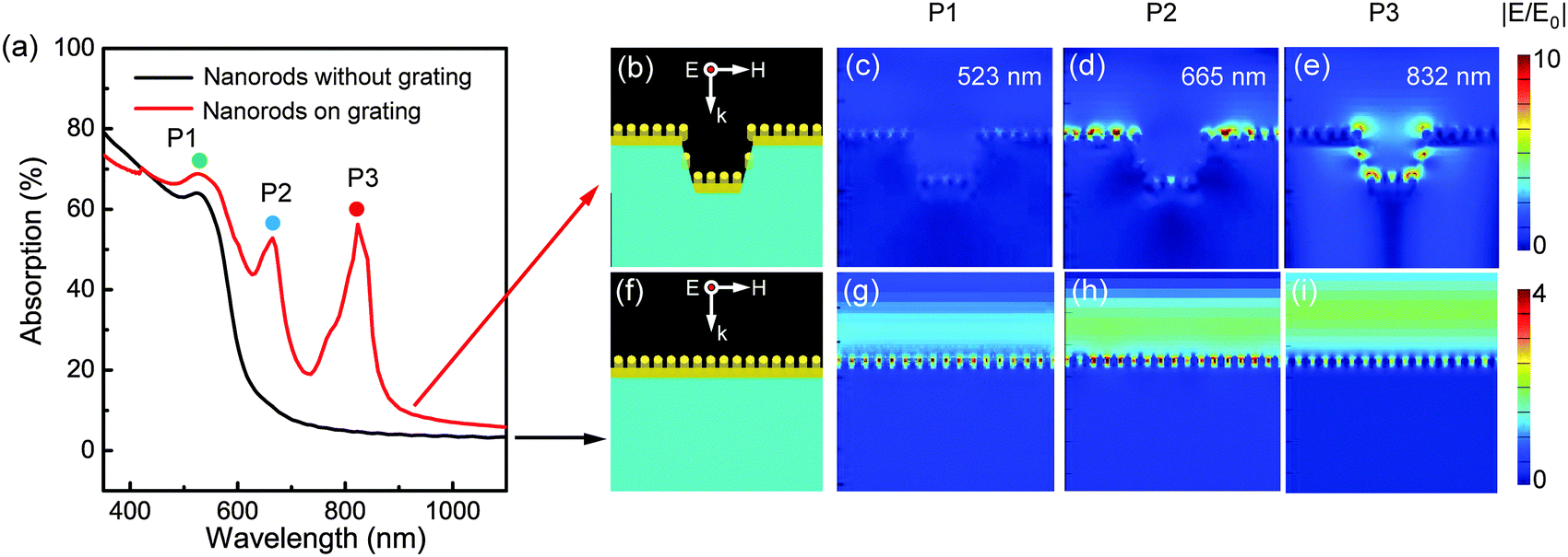 | ||
| Fig. 2 Local hotspots on grating-coupled gold nanorod assembly are much stronger than those on the flat substrate with the same size, shape and rod-to-rod separation. (a) Simulated absorption spectra at normal incidence with p-polarization for the uniform gold nanorod assembly on a grating of PDMS grooves (red curve) and a flat PDMS substrate (black curve), respectively. (b–e) Schematic and simulated electric field intensity distributions of the grating-integrated gold nanorod assembly at P1, P2 and P3 peaks, respectively, at the linear scale. (f–i) Schematic and simulated electric field intensity distributions of the gold nanorod assembly on a flat substrate at the same wavelength, at the linear scale. The sizes of the grating-integrated nanorod assembly are a = 600 nm, h = 150 nm, w1 = 400 nm, w2 = 470 nm, l = 120 nm, d = 25 nm, θ = 15°, sx = 37 nm and sy = 80 nm. | ||
Through controlling the height and periodicity of the PDMS grooves, we can flexibly tune the grating-related plasmon modes (i.e. P2 and P3) of the GIGNs. Fig. 3a shows an evolution of the measured optical absorption under a p-polarized wave at normal incidence, as the height of the groove is varied from 125 to 170 nm (a is fixed to 450 nm). It is clear that P3 shifts from 675 to 746 nm as the height is increased (Fig. 3c), suggesting P3 is associated with the vertical interaction between the top and bottom gold nanorod assemblies while P2 is nearly stable with increasing height, suggesting P2 is a pure lattice-induced mode. In addition, we also examined the influence of the periodicity of the grating on the optical absorption of GIGNs as shown in Fig. 3b. With the increasing periodicity from 350 to 600 nm (h is fixed to 150 nm), the wavelengths of P2 and P3 are both found to red-shift ranging from 529 to 724 nm and 574 to 885 nm, respectively (Fig. 3c). It is believed that these two modes are associated with the in-plane diffractive couplings in air and dielectric, respectively.
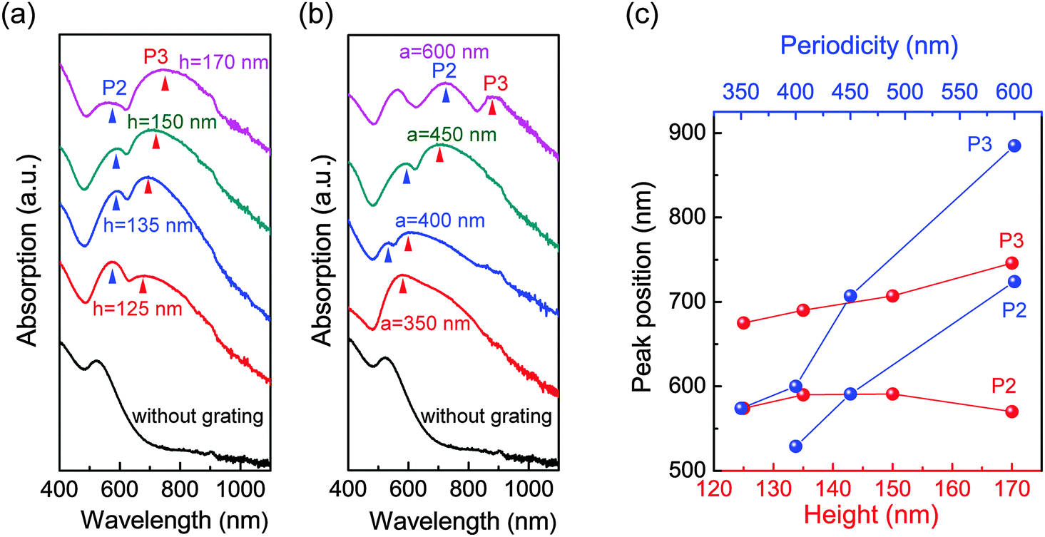 | ||
| Fig. 3 Height- and lattice-dependent plasmon resonances of GIGNs. (a) Measured height-modulated absorption spectra of the GIGNs (a = 450 nm, l = 120 nm, d = 25 nm, θ = 15°, sx = 37 nm and sy = 80 nm). The heights of the grating are 125, 135, 150 and 170 nm, respectively. (b) Measured periodicity-modulated absorption spectra of the GIGNs (h = 150 nm, l = 120 nm, d = 25 nm, θ = 15°, sx = 37 nm and sy = 80 nm). The periodicities of the grating are 350, 400, 450 and 600 nm, respectively. (c) Resonant wavelengths of P2 and P3 as a function of height (red) and periodicity (blue) of the gratings, respectively. | ||
To demonstrate the grating-based modulations on SERS signals, we examined Raman scattering from the Rhodamine 6G (R6G) molecules (Fig. 4a) adsorbed on the samples involved in Fig. 3a and b. To adsorb the target analytes, the surfaces of the substrates were covered by R6G aqueous solution (10−6 M) for 1 h, then washed with deionized water and finally dried with flowing nitrogen. The SERS measurements were performed on a Raman spectrometer (LabRAM HR, HORIBA Scientific). The excitation laser with the wavelength of 633 nm was used. The laser power and signal acquisition time were 0.06 mW and 10 s, respectively. Five measurements were made to determine the standard deviations of the Raman intensity for each sample (the details on adsorptions of probe molecules and SERS measurements can be found in the ESI†). We also measured the SERS spectra under 514 nm excitation, and it is found that, compared to NGIGN, there is no obvious signal amplification effect in GIGN due to the absence of strong coupling between LSPR and Wood’s anomaly near this wavelength (Fig. S4, ESI†). Fig. 4b illustrates the measured SERS spectra taken from the R6G-modified GIGNs, all with a = 450 nm, but with the varying groove heights of 125, 135, 150, 170 and 225 nm, respectively. In addition, the corresponding Raman spectra of the R6G molecules on the NGIGN (red) and pure gold film (black) were also recorded for references respectively. R6G is a kind of dye and has been extensively studied as a model system for SERS sensing. In the measured SERS spectra of R6G, the peaks at 614 cm−1 and 1573 cm−1 are assigned to the C–C–C and C–O–C bond stretching vibrations, respectively. The peaks at 1313, 1361, 1512, and 1649 cm−1 correspond to C–C stretching modes. The peak at 775 cm−1 represents the out-of-plane vibration of deformed C–H bonds.33 As shown in Fig. 4b, compared to the NGIGN and pure gold film, the GIGN presents a remarkable enhancement on Raman intensity. The strongest Raman signal is obtained at the height of 150 nm (dark cyan curve in Fig. 4b). We performed the FDTD simulations on the absorption spectra and electric field intensity distributions of the GIGNs with varying grating height (Fig. S5, ESI†). At the wavelength of the involved P3 mode, as h = 150 nm, the hotspots are localized at both the bottom and side walls of the groove (Fig. S5d, ESI†). In contrast, the shallower and deeper grooves both do not show any hotspots at the side walls of the grooves (Fig. S5c and e, ESI†). It is understood that as h is too small, the grating effect is feeble and the GIGNs are inclined to behave as nanorod assemblies on a flat substrate. When h is too large, the GIGNs begin to weaken the coupling between the top and bottom nanorods. These two effects both hamper the hotspot generation at the side walls of the groove as well as total Ramen efficiency. That is to say, there exists a trade-off in height in approaching the optimal hotspot distributions, for example h = 150 nm in our experiment. At fixed h = 150 nm, we also measured the SERS spectra taken from the R6G-modified GIGNs with various groove periodicities of 350, 400, 450 and 600 nm, respectively (Fig. 4c). The highest Raman enhancement occurs at the periodicity of 400 nm. It is because that the wavelength of P3 mode (600 nm) in the sample with a = 400 nm is closer to the excitation wavelength (633 nm) than the ones with other periodicities. However, the samples with other periodicities also exhibit the high enhancement factors even though slightly lower than the one with a = 400 nm, leading to an inapparent periodicity-based modulation on the SERS intensity. It can be ascribed to the excitation manner in our experiment. In our confocal microscopy system, a large fraction of the focusing light illuminates the sample normally, but it also contains many other components with a series of incident angles (<64°). It means that for a certain periodicity, there always exist some components that can satisfy the conditions of coupling to Wood’s anomalies (P2 or P3 modes)49,50 at the excitation wavelength of 633 nm. For those periodicities, the non-normal-incidence couplings make the main contribution to enhancing the SERS signals. The height- and periodicity-modulated signal enhancements, defined as the Raman intensity ratio of GIGN and NGIGN, are summarized in Fig. 4d. A highest enhancement factor up to 9.6 times is achieved in the GIGN with a = 400 nm and h = 150 nm. Such an enhancement factor mainly arises from the electric field enhancement in P3 mode due to the interaction between the upper and lower gold nanorod assemblies via diffraction in the dielectric grating.
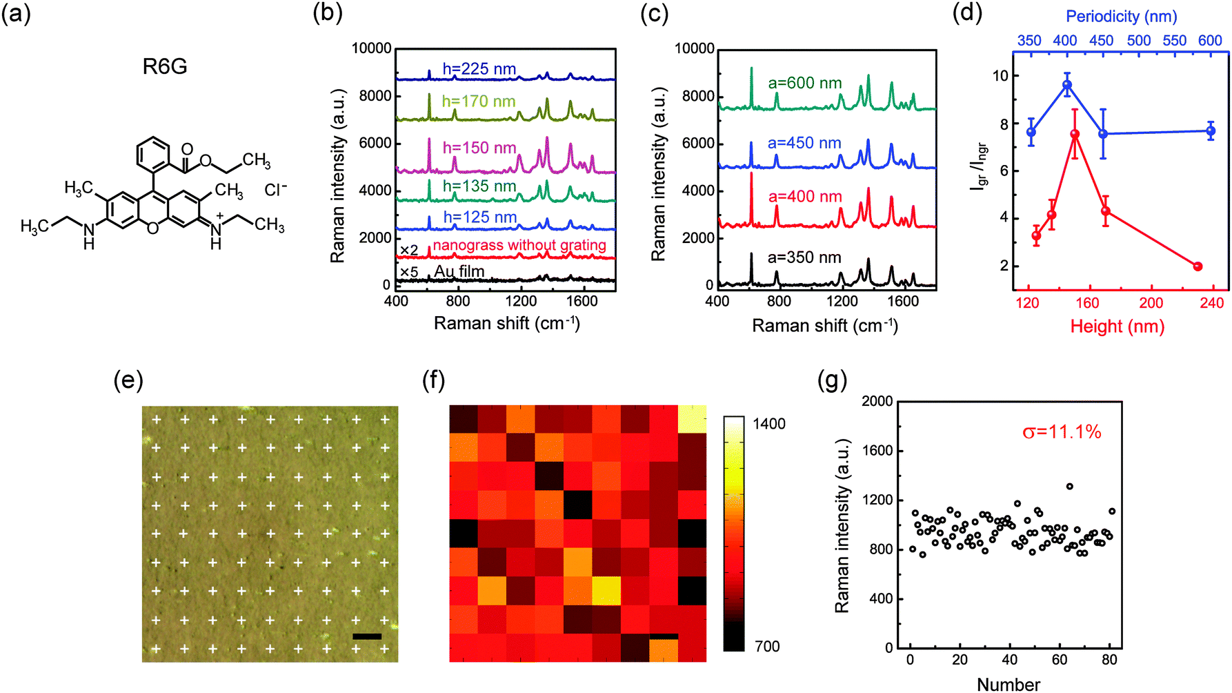 | ||
| Fig. 4 R6G detection. (a) Structural formula of a R6G molecule. (b) SERS spectra of various GIGNs (a = 450 nm, l = 120 nm, d = 25 nm, θ = 15°, sx = 37 nm and sy = 80 nm) with different grating heights of 125, 135, 150, 170 and 225 nm, respectively. The corresponding Raman spectra of the NGIGN (red) and pure gold film (black) were also recorded respectively for references. (c) SERS spectra of various GIGNs (h = 150 nm, l = 120 nm, d = 25 nm, θ = 15°, sx = 37 nm and sy = 80 nm) with different grating periodicities of 350, 400, 450 and 600 nm, respectively. (d) The Raman intensity ratio of the GIGN and NGIGN at the 1361 cm−1 band as a function of height (red) and periodicity (blue) of the grating. (e) Optical micrograph of a GIGN (a = 400 nm and h = 150 nm) covered by R6G molecules. The white crosses represent the collecting points illuminated by the laser spot during the Raman spectra being recorded. The scanning step size is 10 μm. (f) Intensity mapping of R6G for the area as shown in (e) at the 1361 cm−1 band. (g) SERS intensity distribution of R6G in mapping. The relative standard deviation is 11.1% (the relative standard deviations recorded from other more intrinsic Raman peaks are reported in Fig. S6, ESI†). All samples were treated by the R6G aqueous solution with the concentration of 10−6 M. For the height- and periodicity-resolved SERS spectra, the error bars indicate standard deviations of five measurements for each sample. (e and f) Scale bar, 10 μm. | ||
For practical purposes, a uniform and reproducible response is critical for SERS-related applications. In fact, the LSPRs from a single nanoparticle (or aggregate) strongly depend on its geometric factors such as particle size, shape and interparticle gap distance. Surprisingly, in our scheme, the local hotspots can be fully manipulated by controlling the height and periodicity of the loaded dielectric grating. This advantage can substantially eliminate the effect of random fluctuations in the morphology and arrangement of the nanoparticle assemblies. In this regard, this grating-based design is naturally compatible with the low-cost and large-area fabrication methods, such as self-assembly of metal nanoparticles and oblique metal deposition. To demonstrate this inherent benefit of loading a dielectric grating, we performed a SERS intensity mapping of R6G for the GIGN samples (Fig. 4f). In the mapping, the point by point scanning mode with the step size of 10 μm was carried out for the area as shown in Fig. 4e. The measurement configuration at each collection point is identical to the aforementioned description for the R6G detections. Fig. 4f displays the highly uniform SERS intensity mapping of R6G (10−6 M) molecules at 1361 cm−1 bands. According to the statistics at the 1361 cm−1 band, the relative standard deviation of 11.1% is determined (Fig. 4g). This deviation value is remarkably small compared to the traditional metal nanoparticle assemblies on a flat dielectric substrate (∼28%),22 the hierarchical porous metamaterial structure (∼21%)36 and commercial Klarite substrate (∼45%).36 Such an excellent uniformity of SERS signal may be attributed to the following two aspects: first, the local hotspots in our protocol are dominated by the strong coupling between periodically groove-regulated gold nanorod assemblies laterally or vertically rather than the optical properties of an individual gold nanorod. This feature will minimize the effect caused by structural inhomogeneity. Second, our substrate provides a high-density spot distribution (>200 hotpots per μm−2), which improves the uniformity of the SERS signal due to a large reduction in the sensitivity to the hotspot site for target molecules. In addition, we also investigated the reproducibility of GIGNs in terms of sample-to-sample Raman intensity variations. Five samples were fabricated under the same conditions. It can be found that the spectral position of P3 varies within 12 nm among the different samples and a small sample-to-sample relative standard deviation of ∼13% was achieved (Fig. S7, ESI†).
To further demonstrate the versatility and sensitivity of the GIGN, a water-soluble dye, malachite green isothiocyanate (MGITC), was also used. Fig. 5a depicts the SERS spectra of a sample (a = 400 nm, h = 150 nm, w1 = 220 nm, w2 = 280 nm, l = 120 nm, d = 25 nm, θ = 15°, sx = 37 nm and sy = 80 nm) treated by a series of diluted MGITC aqueous solutions with varying concentrations from 10−7 to 10−10 M. The SERS measurement method of this sample for MGITC is identical to what is described above for R6G, with the exception of acquisition time of 20 s. MGITC resonantly absorbs light near the 633 nm wavelength of the excitation source used in the experiments, and its typical vibrational bands at 1180 cm−1 (in-plane benzene ν9 mode), 1367 cm−1 (phenyl-N stretching), 1392 cm−1 (in-plane C–C and C–H stretching) and 1618 cm−1 (phenyl-N + C–C stretching mode) are identified.51 As expected, a decrease in analyte concentrations resulted in a decreasing Raman signal, and at the concentration of ∼10−10 M, the intrinsic Raman peaks of MGITC (763, 801, 918, 1297, 1392, and 1618 cm−1) are very weak but remain observable. The achieved limit of detection approaches down to the level of 100 pM, which is comparable to that of gold nanoparticle assembly on a PMMA template.52 We also performed a mapping of the SERS intensity for MGITC at the concentration of 10−7 M. The deviations of the Raman signal are determined to be around 14% (Fig. S8, ESI†).
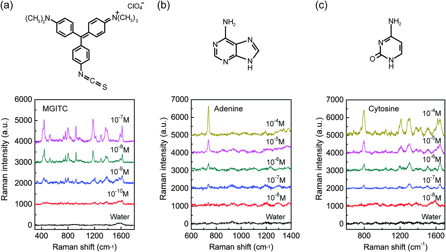 | ||
| Fig. 5 Concentration-dependent SERS spectra recorded for different molecules adsorbed on the GIGNs. (a) MGITC (10−7–10−10 M). (b) Adenine (10−4–10−8 M). (c) Cytosine (10−4–10−8 M). The recorded Raman spectra (black curves) of the GIGNs treated without any target molecules but water are provided for references. The sizes of the GIGNs a = 400 nm, h = 150 nm, w1 = 220 nm, w2 = 280 nm, l = 120 nm, d = 25 nm, θ = 15°, sx = 37 nm and sy = 80 nm. The figures at the top of the panel show the chemical structures of MGITC, adenine and cytosine, respectively. | ||
To investigate their feasibility in biological sensing, we further demonstrated the detection of adenine and cytosine using GIGNs. Adenine and cytosine are two of the four DNA bases, which are parts of the nucleotides in nucleic acids. The detection and identification of these molecules is extremely important for DNA and genome research, such as rapid DNA sequencing and detection of DNA hybridization.53,54 In this study, adenine and cytosine molecules are nonresonant with respect to the laser source. The SERS spectra of adenine and cytosine aqueous solutions with different concentrations (10−4 –10−8 M) are displayed in Fig. 5b and c, respectively (excitation wavelength: 633 nm; laser power: 0.06 mW; and acquisition time: 40 s). The Raman signature peak of adenine at 738 cm−1 in ring breathing mode55 is still distinguishable at the concentration of 10−8 M. Akin to adenine, the characteristic Raman modes of cytosine, such as 796 cm−1 (ring breathing), 1302 cm−1 ((C–NH2) + in-plane (ring)) and 1643 cm−1 (in-plane δ(NH2)),55 are visible for a concentration of 10−7 M. These detection limits at the nanomolar level are comparable to the silver nanoislands on glass nanopillar arrays (10 nM for adenine and 100 nM for cytosine),56 and superior to the silver nanoparticle assemblies on the PMMA fiber tip (215 nM for adenine and 337 nM for cytosine).57 Compared with the patterned glass substrate that requires a relatively expensive step of reactive ion etching, our substrate is low-cost, reproducible (PDMS replica molding) and stable. In addition, considering that silver devices possess higher SERS sensitivities than those for gold ones, the SERS signals could be further improved by replacing GIGNs with the silver counterparts.
Conclusions
In summary, we have developed a grating-integrated strategy for the enhancement of Raman signals of planar SERS-active substrates. Specifically, we have demonstrated the grating-integrated plasmonic nanograss to achieve a 10-fold enhancement factor of Raman signal intensity compared to the same nanograss on a flat substrate. Such a push of SERS sensitivity is attributed to the strong coupling between the periodically grating-regulated gold nanorod assemblies laterally and vertically, which can be totally controlled by tailoring the height and periodicity of the loaded dielectric grating. In addition, the grating-integrated strategy also allows the narrow distributions of spot-to-spot and sample-to-sample SERS signals of the target molecules (relative standard deviations down to ∼11% and 13%, respectively), which is derived from the high-density local hotspot distributions mediated by the dielectric grating and the robust fabrication method, respectively. We have further demonstrated the GIGN as a SERS biosensor for the detection of adenine and cytosine, with their detection limits down to 10 nM and 100 nM, respectively. Finally, our concept presented here provides a universal platform that can be extended to arbitrary metal nanoparticle assemblies or surface roughness systems defined by the low-cost and large-area fabrication methods (e.g. self-assembly or oblique metal deposition). These advantages suggest that our scheme is beneficial for the reliable, sensitive and low-cost SERS-related detection.Acknowledgements
The authors acknowledge the financial support from the National Natural Science foundation of China (11374376, 11174374, 11574406, and 11504437), the Key project of DEGP (No. 2012CXZD0001), Hong Kong RGC (Ref. No.: CUHK1/CRF/12G) and China Postdoctoral Science Foundation (2015M580745).Notes and references
- D. A. Long, Raman Spectroscopy, McGraw-Hill, New York, 1977 Search PubMed.
- S. Nie and S. R. Emory, Science, 1997, 275, 1102–1106 CrossRef CAS PubMed.
- K. Kneipp, W. Yang, H. Kneipp, L. T. Perelman, I. Itzkan, R. R. Dasari and M. S. Feld, Phys. Rev. Lett., 1997, 78, 1667–1670 CrossRef CAS.
- D. K. Lim, K. S. Jeon, J. H. Hwang, H. Kim, S. Kwon, Y. D. Suh and J. M. Nam, Nat. Nanotechnol., 2011, 6, 452–460 CrossRef CAS PubMed.
- M. Fleischmann, P. J. Hendra and A. J. McQuillan, Chem. Phys. Lett., 1974, 26, 163–166 CrossRef CAS.
- Z. Liu, Z. B. Yang, B. Peng, C. Cao, C. Zhang, H. J. You, Q. H. Xiong, Z. Y. Li and J. X. Fang, Adv. Mater., 2014, 26, 2431–2439 CrossRef CAS PubMed.
- J. X. Fang, S. Y. Du, S. Lebedkin, Z. Y. Li, R. Kruk, M. Kappes and H. Hahn, Nano Lett., 2010, 10, 5006–5013 CrossRef CAS PubMed.
- N. A. Hatab, C. H. Hsueh, A. L. Gaddis, S. T. Retterer, J. H. Li, G. Eres, Z. Y. Zhang and B. H. Gu, Nano Lett., 2010, 10, 4952–4955 CrossRef CAS PubMed.
- J. Theiss, P. Pavaskar, P. M. Echternach, R. E. Muller and S. B. Cronin, Nano Lett., 2010, 10, 2749–2754 CrossRef CAS PubMed.
- D. X. Wang, W. Q. Zhu, Y. Z. Chu and K. B. Crozier, Adv. Mater., 2012, 24, 4376–4380 CrossRef CAS PubMed.
- M. Chirumamilla, A. Toma, A. Gopalakrishnan, G. Das, R. P. Zaccaria, R. Krahne, E. Rondanina, M. Leoncini, C. Liberale and F. De Angelis, Adv. Mater., 2014, 26, 2353–2358 CrossRef CAS PubMed.
- H. Lee, J. H. Lee, S. M. Jin, Y. D. Suh and J. M. Nam, Nano Lett., 2013, 13, 6113–6121 CrossRef CAS PubMed.
- H. Im, K. C. Bantz, S. H. Lee, T. W. Johnson, C. L. Haynes and S. H. Oh, Adv. Mater., 2013, 25, 2678–2685 CrossRef CAS PubMed.
- K. D. Osberg, M. Rycenga, N. Harris, A. L. Schmucker, M. R. Langille, G. C. Schatz and C. A. Mirkin, Nano Lett., 2012, 12, 3828–3832 CrossRef CAS PubMed.
- N. Guarrotxena and G. C. Bazan, Adv. Mater., 2014, 26, 1941–1946 CrossRef CAS PubMed.
- T. Ding, L. O. Herrmann, B. de Nijs, F. Benz and J. J. Baumberg, Small, 2015, 11, 2139–2143 CrossRef CAS PubMed.
- P. Kuhler, E. M. Roller, R. Schreiber, T. Liedl, T. Lohmuller and J. Feldmann, Nano Lett., 2014, 14, 2914–2919 CrossRef PubMed.
- V. V. Thacker, L. O. Herrmann, D. O. Sigle, T. Zhang, T. Liedl, J. J. Baumberg and U. F. Keyser, Nat. Commun., 2014, 5, 3448 Search PubMed.
- T. Siegfried, Y. Ekinci, O. J. F. Martin and H. Sigg, Nano Lett., 2013, 13, 5449–5453 CrossRef CAS PubMed.
- J. H. Lee, M. H. You, G. H. Kim and J. M. Nam, Nano Lett., 2014, 14, 6217–6225 CrossRef CAS PubMed.
- H. Y. Liang, Z. P. Li, W. Z. Wang, Y. S. Wu and H. X. Xu, Adv. Mater., 2009, 21, 4614–4618 CrossRef CAS.
- X. Wang, M. H. Li, L. Y. Meng, K. Q. Lin, J. M. Feng, T. X. Huang, Z. L. Yang and B. Ren, ACS Nano, 2014, 8, 528–536 CrossRef CAS PubMed.
- H. Wang, C. S. Levin and N. J. Halas, J. Am. Chem. Soc., 2005, 127, 14992–14993 CrossRef CAS PubMed.
- B. Yan, A. Thubagere, W. R. Premasiri, L. D. Ziegler, L. Dal Negro and B. M. Reinhard, ACS Nano, 2009, 3, 1190–1202 CrossRef CAS PubMed.
- K. Kim, H. S. Han, I. Choi, C. Lee, S. Hong, S. H. Suh, L. P. Lee and T. Kang, Nat. Commun., 2013, 4, 2182 Search PubMed.
- M. P. Cecchini, V. A. Turek, J. Paget, A. A. Kornyshev and J. B. Edel, Nat. Mater., 2013, 12, 165–171 CrossRef CAS PubMed.
- A. Boker, J. He, T. Emrick and T. P. Russell, Soft Matter, 2007, 3, 1231–1248 RSC.
- P. P. Patra, R. Chikkaraddy, R. P. N. Tripathi, A. Dasgupta and G. V. P. Kumar, Nat. Commun., 2014, 5, 4357 CAS.
- H. L. Liu, Z. L. Yang, L. Y. Meng, Y. D. Sun, J. Wang, L. B. Yang, J. H. Liu and Z. Q. Tian, J. Am. Chem. Soc., 2014, 136, 5332–5341 CrossRef CAS PubMed.
- Y. Zhou, X. H. Li, X. G. Ren, L. B. Yang and J. H. Liu, Analyst, 2014, 139, 4799–4805 RSC.
- S. Mahajan, J. J. Baumberg, A. E. Russell and P. N. Bartlett, Phys. Chem. Chem. Phys., 2007, 9, 6016–6020 RSC.
- N. G. Greeneltch, M. G. Blaber, A. I. Henry, G. C. Schatz and R. P. Van Duyne, Anal. Chem., 2013, 85, 2297–2303 CrossRef CAS PubMed.
- P. Wang, O. Liang, W. Zhang, T. Schroeder and Y. H. Xie, Adv. Mater., 2013, 25, 4918–4924 CrossRef CAS PubMed.
- X. N. Wang, Y. Y. Wang, M. Cong, H. B. Li, Y. J. Gu, J. R. Lombardi, S. P. Xu and W. Q. Xu, Small, 2013, 9, 1895–1899 CrossRef CAS PubMed.
- Y. J. Liu, H. Y. Chu and Y. P. Zhao, J. Phys. Chem. C, 2010, 114, 8176–8183 CAS.
- X. Y. Zhang, Y. H. Zheng, X. Liu, W. Lu, J. Y. Dai, D. Y. Lei and D. R. MacFarlane, Adv. Mater., 2015, 27, 1090–1096 CrossRef CAS PubMed.
- X. M. Qian and S. M. Nie, Chem. Soc. Rev., 2008, 37, 912–920 RSC.
- Y. Fang, N.-H. Seong and D. D. Dlott, Science, 2008, 321, 388–392 CrossRef CAS PubMed.
- Y. Z. He, J. X. Fu and Y. P. Zhao, Front. Phys., 2014, 9, 47–59 CrossRef.
- Y. J. Liu, Z. Y. Zhang, Q. Zhao, R. A. Dluhy and Y. P. Zhao, J. Phys. Chem. C, 2009, 113, 9664–9669 CAS.
- Q. Zhou, Y. J. Liu, Y. P. He, Z. J. Zhang and Y. P. Zhao, Appl. Phys. Lett., 2010, 97, 121902 CrossRef.
- J. P. Singh, H. Y. Chu, J. Abell, R. A. Tripp and Y. P. Zhao, Nanoscale, 2012, 4, 3410–3414 RSC.
- L. Polavarapu and L. M. Liz-Marzan, Phys. Chem. Chem. Phys., 2013, 15, 5288–5300 RSC.
- D. Qin, Y. N. Xia and G. M. Whitesides, Nat. Protoc., 2010, 5, 491–502 CrossRef CAS PubMed.
- A. V. Kabashin, P. Evans, S. Pastkovsky, W. Hendren, G. A. Wurtz, R. Atkinson, R. Pollard, V. A. Podolskiy and A. V. Zayats, Nat. Mater., 2009, 8, 867–871 CrossRef CAS PubMed.
- G. A. Wurtz, W. Dickson, D. O'Connor, R. Atkinson, W. Hendren, P. Evans, R. Pollard and A. V. Zayats, Opt. Express, 2008, 16, 7460–7470 CrossRef CAS PubMed.
- W. Dickson, G. A. Wurtz, P. Evans, D. O'Connor, R. Atkinson, R. Pollard and A. V. Zayats, Phys. Rev. B: Condens. Matter Mater. Phys., 2007, 76, 115411 CrossRef.
- T. R. Liu, Y. Shen, W. Shin, Q. Z. Zhu, S. H. Fan and C. J. Jin, Nano Lett., 2014, 14, 3848–3854 CrossRef CAS PubMed.
- W. L. Barnes, W. A. Murray, J. Dintinger, E. Devaux and T. W. Ebbesen, Phys. Rev. Lett., 2004, 92, 107401 CrossRef CAS PubMed.
- H. Gao, J. M. McMahon, M. H. Lee, J. Henzie, S. K. Gray, G. C. Schatz and T. W. Odom, Opt. Express, 2009, 17, 2334–2340 CrossRef CAS PubMed.
- W. N. Leng and P. J. Vikesland, Langmuir, 2014, 30, 8342–8349 CrossRef CAS PubMed.
- L. B. Zhong, J. Yin, Y. M. Zheng, Q. Liu, X. X. Cheng and F. H. Luo, Anal. Chem., 2014, 86, 6262–6267 CrossRef CAS PubMed.
- A. Barhoumi and N. J. Halas, J. Am. Chem. Soc., 2010, 132, 12792–12793 CrossRef CAS PubMed.
- S.-J. Park, A. A. Lazarides, J. J. Storhoff, L. Pesce and C. A. Mirkin, J. Phys. Chem. B, 2004, 108, 12375–12780 CrossRef CAS.
- Y. Badr and M. A. Mahmoud, Spectrochim. Acta, Part A, 2006, 63, 639–645 CrossRef CAS PubMed.
- Y.-J. Oh and K.-H. Jeong, Adv. Mater., 2012, 24, 2234–2237 CrossRef CAS PubMed.
- P. Rajapandiyan and J. Yang, Anal. Chem., 2012, 84, 10277–10282 CrossRef CAS PubMed.
Footnote |
| † Electronic supplementary information (ESI) available. See DOI: 10.1039/c6nh00059b |
| This journal is © The Royal Society of Chemistry 2016 |