
Aligned metal oxide nanotube arrays: key-aspects of anodic TiO2 nanotube formation and properties
Francesca
Riboni
a,
Nhat Truong
Nguyen
a,
Seulgi
So
a and
Patrik
Schmuki
*ab
aDepartment of Materials Science WW4-LKO, University of Erlangen-Nuremberg, Martensstrasse 7, 91058 Erlangen, Germany. E-mail: schmuki@ww.uni-erlangen.de
bDepartment of Chemistry, Faculty of Science, King Abdulaziz University, P.O. Box 80203, Jeddah 21569, Saudi Arabia
First published on 26th May 2016
Abstract
Over the past ten years, self-aligned TiO2 nanotubes have attracted tremendous scientific and technological interest due to their anticipated impact on energy conversion, environment remediation and biocompatibility. In the present manuscript, we review fundamental principles that govern the self-organized initiation of anodic TiO2 nanotubes. We start with the fundamental question: why is self-organization taking place? We illustrate the inherent key mechanistic aspects that lead to tube growth in various different morphologies, such as ripple-walled tubes, smooth tubes, stacks and bamboo-type tubes, and importantly the formation of double-walled TiO2 nanotubes versus single-walled tubes, and the drastic difference in their physical and chemical properties. We show how both double- and single-walled tube layers can be detached from the metallic substrate and exploited for the preparation of robust self-standing membranes. Finally, we show how by selecting specific growth approaches to TiO2 nanotubes desired functional features can be significantly improved, e.g., enhanced electron mobility, intrinsic doping, or crystallization into pure anatase at high temperatures can be achieved. Finally, we briefly outline the impact of property, modifications and morphology on functional uses of self-organized nanotubes for most important applications.
 Francesca Riboni | Francesca Riboni studied Chemical Sciences at the University of Milan, Italy, and obtained her PhD in Chemistry from the University of Milan, Italy, in 2014. She joined the group of Prof. Schmuki at the University of Erlangen-Nuremberg, Germany, in 2015 as a postdoctoral fellow. Her research interests include the synthesis of functional nanomaterials by electrochemical processes and their application as energy conversion and storage devices. |
 Nhat Truong Nguyen | Nhat Truong Nguyen studied Chemical Engineering at Ho Chi Minh University of Technology, Vietnam and obtained his MSc degree in Material Engineering from University of Science and Technology, Korea, in 2012. He is currently a PhD student in the group of Prof. Schmuki at the University of Erlangen-Nuremberg in Germany. His research interests include the synthesis and functionalization of semiconductor nanomaterials for energy conversion applications. |
 Seulgi So | Seulgi So obtained her MSc degree in Materials Chemistry from Korea University, Korea in 2011 and her PhD degree in Materials Science and Engineering from University of Erlangen-Nuremberg, Germany, in 2015. She worked as postdoctoral fellow in the groups of Prof. Schmuki at the University of Erlangen-Nuremberg, Germany, and of Prof. Sadoway at the Massachusetts Institute of Technology, US. She is currently a postdoctoral fellow in the group of Prof. Corn at the University of California Irvine, US. Her research interests include the synthesis of functional nanomaterials by electrochemical processes and their application in various energy conversion fields. |
 Patrik Schmuki | Patrik Schmuki obtained his PhD from ETH Zurich, Switzerland, in 1992. From 1994–1997 he worked at Brookhaven National Laboratory, US, and at the Institute for Microstructural Sciences of the National Research Council of Canada. From 1997–2000, he has been an Associate Professor for Microstructuring Materials at EPFL, Switzerland, and since 2000 he has been Full Professor and Head of the Institute for Surface Science and Corrosion at the Department of Materials Science and Engineering of the University of Erlangen-Nuremberg. His research interests target electrochemistry and materials science at the nanoscale, with a particular focus on functional materials and self-organization processes. |
1. Introduction
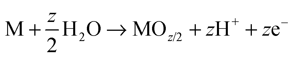
One-dimensional (1D) nano-architectures exhibit a unique set of properties that attracts a great deal of scientific and technological interest. In particular, 1D-nanotube (NT) arrays have gained increasingly more attention as they provide an exceptional combination of optical, electrical and chemical properties with extreme geometry that has inspired remarkable advances in recent nanotechnology and microelectronics. Compared to bulk materials, NTs can feature characteristics such as high electron mobility and quantum size related effects, along with very high specific surface area and mechanical strength that are highly relevant for numerous applications in physics, chemistry, materials science, and medicine.1–4Upon the discovery of carbon nanotubes,5 and following their large impact on nanotechnology,6–12 research efforts have also been extended to a large number of inorganic materials, mainly oxides and sulfides of metals and transition metals.13–19 For oxide/sulfide nanotubes, a variety of synthesis routes has been reported such as hydrothermal,20–22 sol–gel or template-assisted methods.23–26 In recent years, another most frequently adopted and straightforward approach for growing highly ordered 1D-nanostructures is self-organizing electrochemical anodization (SOA).27,28 It allows the fabrication of vertically oriented, size-controlled and back-contacted (i.e., anchored to a metallic substrate) nanostructured arrays (e.g., aligned pores, nanochannels, and nanotubes) on various metals and alloys (Fig. 2).29–37 As illustrated in Fig. 1a and b and described in more details in the following sections, anodizing can be carried out in a simple anode/cathode arrangement, where the metal of interest (M) serves as anode. The oxide growth process is based on the oxidation of M (M → Mz+ + ze−) and its conversion to metal oxide (MOz/2) under a suitable voltage, the source of oxygen ions being typically H2O in the electrolyte.
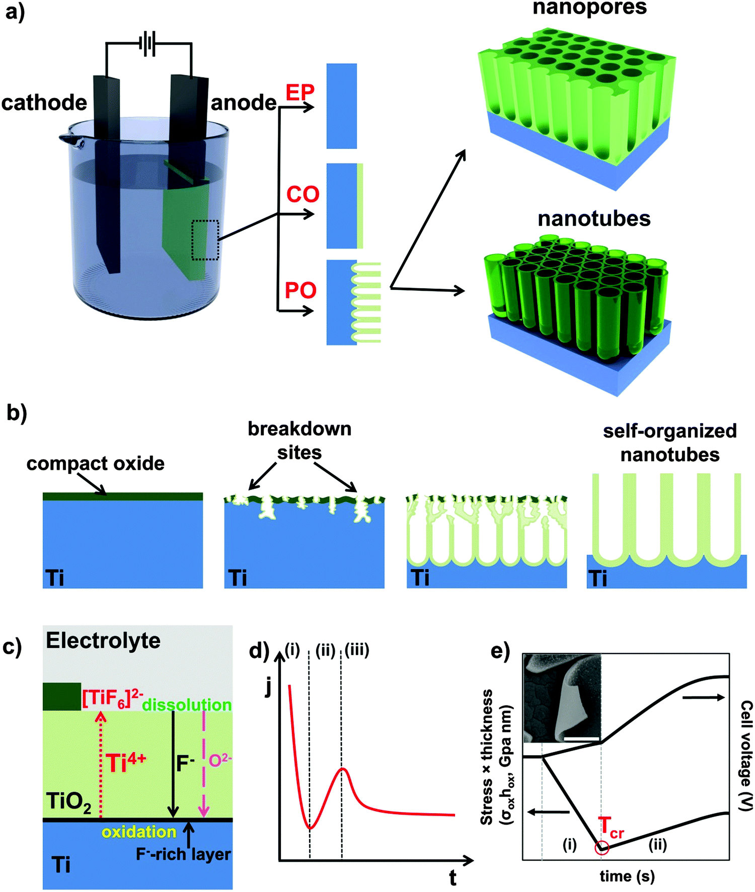 | ||
| Fig. 1 (a) Typical 2-electrode electrochemical anodization set-up and possible anodic morphologies: (EP) metal electropolishing, (CO) formation of a compact anodic oxide, (PO) self-ordered nanostructured oxide (nanopores or nanotubes). (b) Schematic representation of the TiO2 nanotube formation process: first a compact layer is grown; afterwards, breakdown of the barrier film occurs and an ordered porous structure, covered with the thin initial layer, forms; finally, under an optimized set of experimental parameters, regular self-organized TiO2 nanotubes are obtained. (c) High field oxide formation in the presence of fluoride ions: a steady-state is established between the oxide formation at the inner interface and its dissolution at the outer interface (due to dissolution/complexation of Ti4+ as TiF62−). Rapid fluoride migration leads to the formation of a fluoride-rich layer at the Ti/TiO2 interface. (d) Typical current–time (j–t) characteristics and different stages in nanotube formation: (i) initial formation of a compact oxide layer; (ii) initiation of irregular nanoscale pores under optimized anodizing conditions; (iii) formation of a regular nanoporous/nanotubular layer. (e) Time evolution of stress × thickness (σoxhox, left axis) and cell voltage (right axis) during self-organizing anodization of a Ti thin film under galvanostatic condition. The inset shows the instantaneous roll-up of a thin NT layer (∼200 nm) detached from the metallic substrate that is indicative of a residual compressive stress (scale bar of the SEM image 5 nm). | ||
Historically, landmarks on the growth and use of such electrochemical nanostructures were certainly represented by the initial reports of Rummel38 and Baumann39 on the fabrication of porous-type aluminum oxide layers, and by the work of Thompson and Wood40 who first highlighted the great potential of porous alumina for organic dyes or inorganic pigment loading as well as corrosion protection. Another cornerstone towards functional uses of porous alumina was the report of Masuda et al. in 1995 that demonstrated a virtually perfect hexagonal arrangement of closely-packed cells if porous alumina is grown under optimized conditions in acidic electrolytes.41 Over the last 20 years, porous alumina has been extensively applied as a template for the synthesis of functional nanomaterials, particularly for the fabrication of nanorods, nanowires and nanotubes by deposition of metals, semiconductors or polymer materials.41–45 In addition, also the direct use of nanoporous Al2O3 for decorative, wear- and corrosion-resistant applications, as a filter or as a photonic crystal, has been strongly developed.46 Over decades, aluminum was considered the only metal that can form anodic self-ordered oxide structures and early works by Assefpour-Dezfuly47 and Zwilling48 on TiO2 nanotube formation on Ti went almost unnoticed. A few years later, this type of first generation of TiO2 nanotubes grown in acidic aqueous electrolytes was further investigated and essentially confirmed the earlier findings.49,50 However, all these layers were not highly organized, limited in length to ∼500 nm, and with considerable wall inhomogeneity, but anyway proved that the key-factor for growing self-organized TiO2 nanotubular arrays is the addition of fluoride species to the electrolyte. Reasoning for this specific role of fluorides is that they provide the feasibility to establish an equilibrium between anodic oxide formation and chemical dissolution (Ti4+ is relatively easily solvatized by F− in the form of [TiF62−]). Further significant improvements were the introduction of electrolyte pH mediation,51 the use of non-aqueous fluoride electrolytes (glycerol, ethylene glycol, DMSO),52–55 and fine tuning of voltage control and alteration procedures,56–58 that allowed a higher degree of self-ordering and a strongly enhanced morphology control. Progressively, the use of fluoride-based electrolytes was shown to enable the growth of similar nanotubular anodic oxides also on a wide palette of metals, such as Fe,59–61 W,62,63 Nb,64,65 V,66 Co,67 Ta,68–71 Zr,72–74 Hf75,76 as illustrated in Fig. 2 and even metal-alloys, such as Ti–Nb,29,77–82 Ti–Zr,83 Ti–Ta,34,84–86 Ti–W,37 Ti–Cr,87 Ti–Mo,88 Ti–V,78 Ti–Ru.89 In particular, anodizing metal-alloys turned out to be a unique and elegant way of direct doping the tube oxide layer by introducing well-defined amounts of a secondary species in the oxide, or to intrinsically decorate tubes with noble metal nanoparticles.90,91
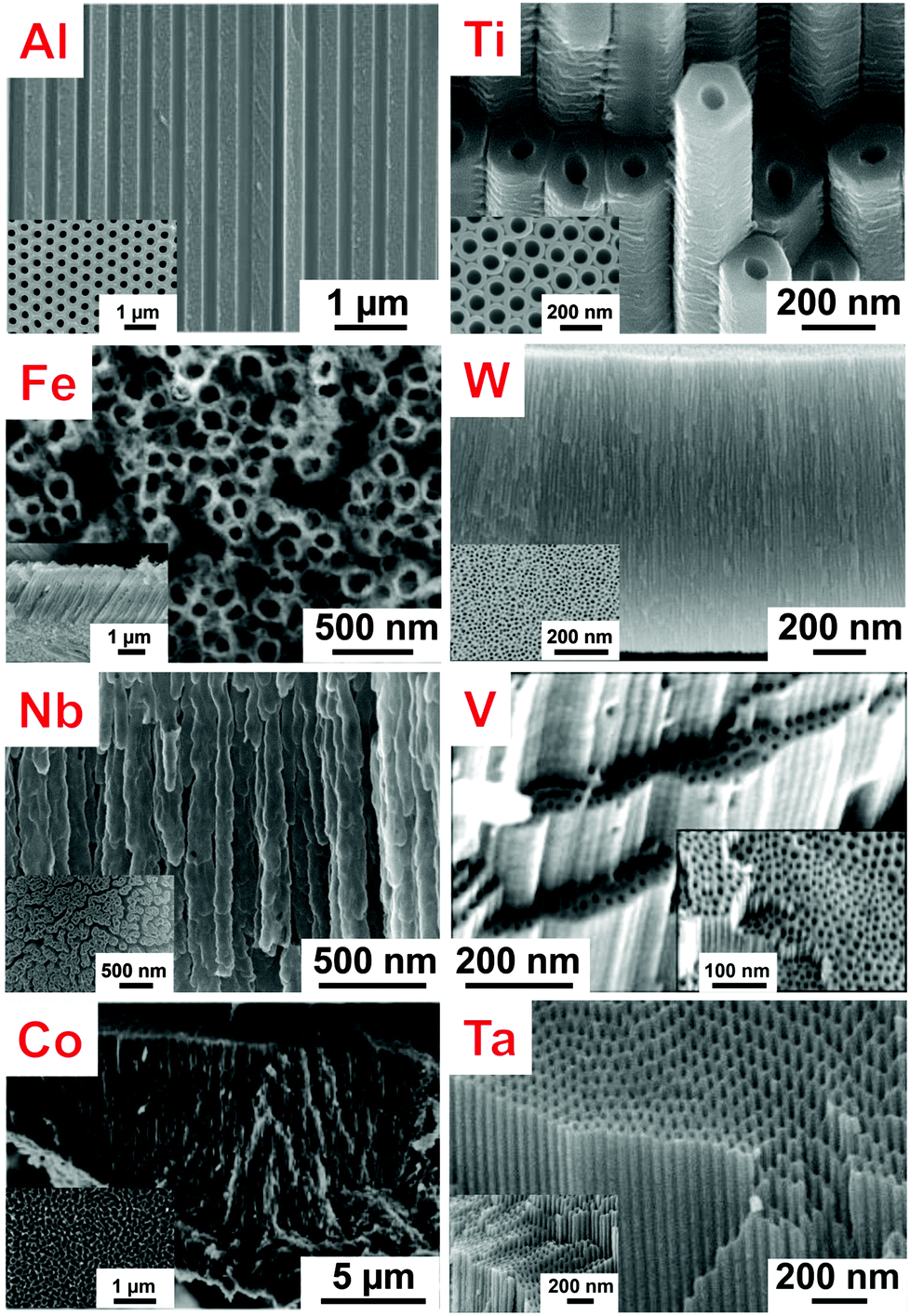 | ||
| Fig. 2 SEM images illustrating the structure of ordered oxide nanotube and nanopore layers electrochemically grown on different valve metals. Al: Reproduced with permission from ref. 33. Ti: Reproduced from ref. 146 with permission from the Royal Society of Chemistry; inset: Reproduced with permission from ref. 150. W: Reproduced with permission from ref. 98. Nb: Reproduced from ref. 65 with permission from the Royal Society of Chemistry. V: Reproduced with permission from ref. 66. Co: Reproduced with permission from ref. 67. Ta: Reproduced with permission from ref. 35. | ||
Owing to the extended control over nanoscale geometry, direct back-contacting, and due to the large versatility of this approach to grow nanotubular structures of various metal oxides and mixed oxide compounds, electrochemical anodization is in many cases a most straightforward nanotube synthesis path. Therefore, self-organized nanotubular structures find application in a variety of fields: TiO2 nanotubes are extensively investigated in solar cells (DSSCs), photocatalysis and biomedical applications, α-Fe2O3 and Ta3N5 NTs as anode for (photo)electrochemical water splitting reactions,60,61,92–95 ordered nanoporous V2O5 and Co3O4 structures for batteries and ion intercalation devices or as oxygen evolution catalysts,66,67 WO3 nanochannels for gas sensing and electrochromic applications,96–98etc.
However, TiO2 represents by far the most investigated metal oxide.28,50,60,65,66,98,99 This can be ascribed to the outstanding breadth of properties of this compound: classically used for its non-toxic, environmentally friendly, corrosion-resistant and biocompatible characteristics, many functional applications rely on the specific ionic and electronic properties of TiO2. Among these, a wide range of photo-electrochemical applications (photocatalytic splitting of water into oxygen and hydrogen, self-cleaning surfaces, organic pollutant degradation) or the use of TiO2 in solar cells (most frequently in Grätzel-type DSSCs) are most common.100,101 Aligned one-dimensional arrangements are particularly beneficial for the performance in (photo)electrochemical applications, as orthogonal carrier separation in these structures is facilitated, i.e., electrons and holes are driven apart (that is, e− are collected at the back contact and h+ accumulated at the semiconductor/electrolyte interface). This particularly helps overcoming the limitations of a short diffusion length of holes in TiO2 (∼10 nm) while exploiting the comparably long electron diffusion length (∼20 μm in TiO2 nanotubes).102 As TiO2 nanotubular structures simultaneously combine the highly functional features of TiO2 with a regular and controllable nanoscale geometry (that is, tube-length, -diameter, and self-ordering that can be tailored over large length scales), intense research activities have been devoted to anodic TiO2 nanotubes over the last ten years (see, for instance, research trends reported in ref. 28 and 103).
While a number of recent reviews focus on properties and applications of TiO2 nanotubes and other aligned channels,27,28,104 the present review mainly focuses on mechanistic aspects of nanotube growth and self-organization: why do tubes (not pores) form, what are the critical factors to achieve self-organization and how to improve it, why is the tube wall morphology sometimes rippled sometimes smooth, how to grow multi-layered tubes, why are single-walled TiO2 nanotubes so superior compared to double-walled tubes? Along with the factors determining nanotube formation and leading to various tube morphologies, we will also briefly discuss the significance of various types of tubes and tube features for electric, electronic and optical properties that in turn dramatically affect the performance of tube arrays in virtually any (photo)electrochemical application.
2. Stages and key aspects of nanotube formation
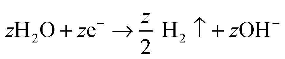
As mentioned, anodization is frequently carried out in a 2-electrode electrochemical arrangement as illustrated in Fig. 1a, with the metal of interest (M) as working electrode (anode) and a counter electrode (typically platinum or carbon) as cathode. Overall, the process can be described in terms of following equations:| M → Mz+ + ze− | (1) |
 | (2) |
| 2H2O → O2(g) + 4H+ + 4e− | (3) |
 | (4) |
On various metals (valve metals), oxidation (1) and conversion to a thick metal oxide (2) can be achieved in an aqueous electrolyte at sufficiently high anodic voltages. For non-valve metals, only thin oxides can grow, as O2 evolution (3) is the preferred anodic reaction.27,104,105 In either case, a counter reaction, typically the reduction of H+ (from the electrolyte) to gaseous H2(4), takes place at the cathode.27,28 Depending on the electrolyte and on several anodization conditions, three different scenarios are possible: (i) if the oxide is completely soluble (Mz+ ions are entirely solvatized) in the electrolyte, the layer is continuously etched and metal corrosion (or electropolishing, EP) is observed (Fig. 1a, EP); (ii) if the formed oxide is entirely insoluble in the electrolyte, a compact oxide (CO) layer is formed on the surface of the metal (Fig. 1a, CO); (iii) if the oxide is partially soluble (Mz+ cations can be solvatized) and under a specific set of experimental conditions, a steady-state between oxide formation and dissolution can be established and a porous or tubular metal oxide can grow (Fig. 1a, PO).
Mechanistically, anodic oxide formation is controlled by a high-field ion formation/transport process, where the kinetics of oxide growth (at the metal/oxide or at the oxide/solution interface) depends to a large extent on the rate of ion migration where Mz+ migrates with the field outward and O2− (abstracted from water) inward (see Fig. 1c). Ion movement is influenced by the relative mobility of the cation and the anion in the oxide. Accordingly, the film can grow at the inner and outer interface.106 Generally, the overall oxide growth (as long as high field conditions hold) is related to the electric field (E = ΔU/d) applied across the oxide layer:
I = A![[thin space (1/6-em)]](https://www.rsc.org/images/entities/char_2009.gif) exp(BE) = Aexp(BΔU/d) exp(BE) = Aexp(BΔU/d) | (5) |
 | (6) |
| Experimental parameters | TiO2 nanotubes | Ref. | |||
|---|---|---|---|---|---|
| Length | Diameter | Additional features | |||
| Electrolyte | H2O-based | Max ∼2.5 μm (limited thickness due to high chemical etching rate) | 10–150 nm (voltage-dependent) |
– Rippled-walls
– Longer tubes grown at neutral pH |
220 |
| • H3PO4/HF | 20 nm−1 μm (1–25 V, 0.3 wt% HF) | 15–120 nm (1–25 V, 0.3 wt% HF) | 144 | ||
| 200 nm (15 V, 3 M HF) | 80 nm (15 V, 3 M HF) | – Highly ordered and short aspect ratio NTs | 158 | ||
| Organic-based | Up to several 100 μm | Up to 800 nm | – “nanograss” formation on NT tops, due to long anodization time | 157 | |
| • Ethylene glycol | Dependent on anodization time and applied voltage | V-shaped morphology (i.e., thinner wall at NT top) |
– Double-walled NTs
– Carbon-rich layer (inner shell) |
221, 222 | |
| • DMSO | ∼15 μm | 200 nm | – Single-walled NTs | 54, 55, 157 | |
| • F− content | Thicker layers are grown at higher F− conc. (e.g., 25–30 μm, 0.2 M HF − 120 V) | Depends to a certain extent on the F – conc. due to chemical etching | – For too high F− amount, electropolishing takes place | 128 | |
| • H2O content | Highly ordered nanotube arrays for limited H2O amount | Larger diameter with higher H2O content | – Smooth wall NTs (no ripples) | 52, 222 | |
| Temperature | • Low (10 °C) | Slower growth rate (∼7 μm) | 200–230 nm | – Nanocolumn structure at T < 10 °C | 223 |
| • High (>20 °C) | Faster growth rate (∼11 μm) | ∼150 nm | |||
| Additive complexing agent | • EDTA | Fast growth rate (41 μm h−1) | ∼180–200 nm | – No dielectric breakdown events (comparably high voltage, e.g. 120 V, can be applied) | 224 |
| • Lactic acid | Fast growth rate (20 μm min−1) | 220 nm | 225 | ||
| Anodization voltage | • Constant | Linear dependence on applied voltage | –Morphology depends on the electrolyte | 222 | |
| • Alternating | – Bamboo-type, branching-type | 57, 226 | |||
| Anodization time | • Short time | Anodization time influences the NT length, until a steady-state between their growth (at the bottom) and the chemical etching (at the top) is established | – Formation of initiation layer | 222 | |
| • Long time | – Formation of nanograss, due to etching of tube wall | 112 | |||
| Patterned substrates | • Two-step anodization | Maximizing ordering and ideal arrangements | 160, 167, 171 | ||
| • FIB | |||||
| • Nanoimprinting | |||||
A versatile tool to describe thermodynamics and kinetics of electrochemical reactions are current–voltage curves (where the potential can be regarded as thermodynamic axis and the current as kinetic axis).112 To monitor the evolution of nanotubes over time, it is interesting to follow j–t curves. A typical current–time curve (Fig. 1d) that describes the conditions to nanotube formation can be divided into three sections: (i) in the early stage of anodizing, a compact oxide layer is formed; as the barrier layer thickens, j accordingly decreases (this, in line with (5)); (ii) under optimized growth conditions (Table 1), irregular nanoscale pores penetrate into the initial compact oxide; here, the current rises as the reactive area (exposed to the electrolyte) increases; (iii) a regular nanoporous/nanotubular layer forms and the current drops again until a steady-state situation is established between oxide formation at the metal/oxide interface and the dissolution at the oxide/solution interface (Mz+ ions from dissolved oxide and ions directly ejected from the oxide by the high field are solvatized by F−, (6)). Due to this dissolution, a current significantly higher than that corresponding to compact oxide formation (assuming the same applied voltage) is observed. According to (5), this means that under steady-state condition for tube growth a higher field is present at the tube bottom (that drives ion migration).
However, except for this steady-state formation–dissolution equilibrium, a second key factor to tube formation is the buildup of compressive stress during the early stages of anodic oxide formation. As predicted by the Pilling–Bedworth (PB) ratio (Φ, the ratio of oxide volume created by oxidation vs. the metal volume consumed),113 stress is generated by volume expansion (for many metal/oxide systems) when converting the metal to oxide and is due to the constraint of volume conservation at the metal/oxide interface. This stress is present in any anodic film but, if a compact layer is formed, the stress remains “frozen in” or leads to some cracks in the oxide layer. In situ measurements of internal stress evolution (Fig. 1e) reveal that two different characteristic stages are observed when anodizing a metal substrate: in the first stage, a relatively large compressive (d(σoxhox)/dt < 0) internal stress, in the range of 2–4 GPa for anodic TiO2, is observed that has been, except for the PB effect, also attributed to oxygen evolution (OER) from the electrolyte that occurs inside the oxide film. Here the anodization efficiency (ε, that corresponds to the fraction of oxidized metal ions retained in the final anodic film relative to the film dissolution)113 is comparably low (i.e., low dV/dt and ε ∼ 10–20%) as the majority of charge is consumed in the anodic side reaction (OER). The presence of an overall residual compressive stress in the tube layers is most evident from the instantaneous roll-up of thin NT layers when removed from the substrate (inset of Fig. 1e). When the anodic film thickness reaches a certain value (critical thickness, Tcr), OER ceases due to kinetic limitations. At this stage, also the compressive stress disappears and in some cases, an instantaneous tensile stress component is observed. (i.e., to maintain a compressive stress situation, the oxide should not grow thicker than Tcr).114 Or, in other words, only if a steady-state “formation–dissolution equilibrium” is established, compressive stress can permanently act on the continuously formed oxide and finally, in a flow mechanism, shift the oxide up to form tube walls as described in more detail below. Also, it should be noted that during oxide growth a second component of stress, i.e. electrostrictive stress, is acting on the anodic system. The extent of this is not only strongly voltage- but also material-dependent.115,116
2.1 Pore initiation and nanopattern selection
As pointed out above, during self-ordering electrochemical anodization essentially four concomitant reactions occur: (i) formation of metal ions upon metal substrate oxidation (1), (ii) generation of O2− from the reaction of H2O at the film surface (3), (iii) dissolution and loss of metal ions to the electrolyte, driven by field-assisted cation ejection (5), and (iv) chemical dissolution of the film (6). Arguments (i) and (ii) are responsible for forming the film, while (iii) and (iv) lead to oxide loss.Experimentally, in the very early stage of anodization, first the formation of a few nanometer-thick conformal, compact oxide layer (often referred to as “barrier layer”) takes place. Then, morphological instabilities occur, such as a corrugated surface (Fig. 3a). This process leads to a stochastic distribution of sites with “thinned” oxide locations – this surface pattern is in a lateral length scale of some nm to some 10 nm.108,111 This causes electrochemical processes to occur accelerated at the thinner parts of the layer, that is, in the “valleys” (Fig. 3a) where the intensity of the applied electrochemical field is enhanced (5). Noteworthy, at these most active sites also the generation of H+ is enhanced ( ), which may additionally affect the local chemical dissolution (thinning) of the oxide (6).32,108,117
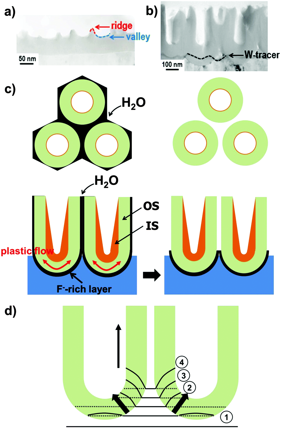 | ||
| Fig. 3 (a) TEM micrograph of an anodic alumina film after anodization, where “ridges” and “valleys” are highlighted. Reprinted with permission from J. Electrochem. Soc., 2010, 157(11), C399. Copyright 2010, The Electrochemical Society. (b) TEM image of Al2O3 nanopores with a tungsten tracer layer. Reprinted with permission from Electrochem. Solid-State Lett., 2006, 9(11), B47. Copyright 2006, The Electrochemical Society. (c) Schematic of TiO2 nanotube formation: displacement of the fluoride-rich layer towards the cell boundaries by a plastic flow mechanism (left-side) and dissolution of the fluoride-rich cell boundaries and consequent formation of nanotubes (right-side). (d) Schematic of the field concentration effects at the bottom of anodic nanotubes and model for length expansion: stress pushes some of the oxide up in the direction of tube walls. Reprinted with permission from J. Electrochem. Soc., 2007, 154(9), C472. Copyright 2007, The Electrochemical Society. | ||
Linear stability analysis, based on perturbation analysis118,119 or numerical treatments,113 indicate that compressive stress in a thick anodic oxide (compact oxide) is rather small and not sustained by a certain flux of ions (electromigration) across the film/electrolyte interface (i.e., formation–dissolution equilibrium). Therefore, only for thin films, conditions are provided for stress evolution sufficient for anodic pattern formation. As outlined above, this is also dictated by oxide dissolution at the oxide/electrolyte interface. Time-evolution of this interface is a function of electric potential, ϕ (i.e., the driving force for metal-ion transport), and of oxygen chemical potential, μOX (or driving force for oxygen-ion transport). Both ϕ and μOX are uniform at the oxide/solution interface, that is, ϕ is set to zero as all the small potential drops through the interfacial electrical double layer do not affect the interface dynamics, and μOX is also zero as the oxide surface is assumed stress-free; therefore, ϕ and μOX gradients within the film are distorted. In particular, their gradient is maximized at valleys and attenuated at ridges (Fig. 3a). Correspondingly, both metal and oxygen ions migrate more rapidly at valleys than at ridges. However, given a distinct volume change when a specific metal is converted to oxide (corresponding to a certain Pilling–Bedworth ratio Φ), only a limited set of parameters, and thus of efficiency ε, applies for pattern selection and formation of nanoporous film. For instance, in the case of TiO2, ε = 0.50–0.65 was determined under various experimental conditions for nanotube growth,120 which is in good agreement with theoretical predictions.113 According to this model, if the efficiency lies outside the predicted range, no ordered nanotubes would be obtained. In particular, at lower efficiencies the fraction of oxidized metal atoms retained in the oxide is small and, therefore, the dynamics of the oxide/solution interface is dominated by oxygen migration that leads to valleys recession and deepening, destabilizing the interface (i.e., extensive etching of the oxide and, ultimately, corrosion and/or electropolishing are observed). By contrast, at higher efficiencies the interface evolution is regulated by the deposition rate of new oxide and the upper limit is represented by ε approaching 100%, where a compact (thickness-limited) anodic film is formed as any depressions on the oxide/solution interface instantly fill with new material. Thus, nanoporous pattern selection (i.e., an optimal ε range) is governed by a combination of oxygen flow (μOX), responsible for destabilizing the interface, and of metal ion flow (ϕ) that promotes stability.113,120,121
2.2 Growth of nanostructured oxide
Further steady growth of nanotubes is explained in literature by two common models: (i) either assuming an enhanced field-assisted dissolution of titania along with a field-assisted ejection of Ti4+ ions at the base of the pores,122–124 or (ii) a field-assisted viscous flow of film material from the barrier layer towards the cell wall regions.106,125–127 In either case, field enhancement at the curved bottom oxide (Fig. 3d) or flow, self-organization can be achieved only for an optimized set of parameters (e.g., applied potential, current density, temperature and fluoride concentration)128 which in turn reflect that a set of conditions needs to be established to adjust an optimal oxide formation–dissolution equilibrium. This is consistent with the frequent observation of a tube-bottom-oxide layer that is thinner than an equivalent compact oxide under the same applied voltage conditions. The final thickness of compact anodic oxide on Ti is usually d = f × U.108 In other words, the thinner oxide at the tube bottom reflects that a high field is present that cannot be lowered by oxide growth as the corresponding dissolution rate prevents this. In pure field driven models, such as established by Gösele et al.,129 the enhanced field (see distribution in Fig. 3d) promotes ejection of Ti4+ species to the electrolyte and this would be a sufficient condition for continuous growth. However, recently established models estimate that the forces in the growing oxide are sufficiently high to cause viscous flow of the oxide. While a number of arguments such as the introduction and distribution of incorporated electrolyte ions can be explained by both approaches, there are a number of findings supporting the presence of a field-assisted flow:(i) An experiment carried out using a thin W-tracer layer in an Al substrate and then growing Al2O3 nanopores through this127,130 (similarly for TiO2 nanotubes)106 showed a flow-type distribution of the tungsten metal oxide tracer from the barrier layer towards and up the cell walls (Fig. 3b).
(ii) Some reports present data that, at this stage of the tube growth, cation ejection to the electrolyte is negligible131 and inward migration of anion species mainly contributes to the ionic current in the high-field barrier oxide. Therefore, the formed oxide must be pushed out of the way, i.e. up the wall.
(iii) The nanotube or nanopore film thickness (the tube length) exceeds the expected thickness of a corresponding compact oxide. For anodic TiO2, the thickness of a compact film is 2.43 times that of the consumed titanium (corresponding to the Pilling–Bedworth ratio (PBR)). The PBR can be measured or calculated assuming a certain oxide density.106 If the oxide growth would be ruled by a high field oxidation process only, then the tube or pore length would be 2.43 times the amount of metal consumed. Nevertheless, for Al and Ti the corresponding tubes or pores are longer. (According to models that are restricted to the high field oxidation, an explanation of this finding requires an assumption of an oxide density that is lower than usually reported for amorphous anatase or rutile material.)106 In flow models, this length extension is ascribed to a stress-induced viscous flow of oxide vertically to the metallic film. In other words, TiO2 nanotube growth occurs, at least partially, by a flow of TiO2 up the wall (any lateral expansion of the oxide is negligible).132 This is illustrated in Fig. 3d where broken and solid lines represent the position of the atoms before and after oxidation, respectively. As the reaction proceeds (stages 1–4), increasingly larger stress is generated in the oxide (i.e., solid lines bend to the vertical axis) and the bent location shifts to the center between two adjacent tubes.108,126,132,133 Measured expansion factors, Fm (estimated as the thickness of the film relative to that of the oxidized metal) can be expressed as a function of the total volume of the film (P), influenced by incorporated contaminants (k):
 | (7) |
2.3 Nanopores vs. nanotubes
A main difference in porous alumina and TiO2 nanotubes is that, for TiO2, the tube morphology is created by the presence of a fluoride species and the formation and dissolution of a fluoride rich layer at the bottom and around the tubes. In terms of tube growth, the formation of a fluoride-rich layer at the tube bottoms and walls can be explained by the fact that F− ions compete with O2− inward migration (Fig. 1c) and that the rate of inward migration of F− ions is clearly higher than that of O2−.134 As a result, a TiF4 (or oxyfluoride) layer forms at the metal/oxide interface. As anodization proceeds, this layer also decorates the tube walls (Fig. 3c).106,127 Experimental evidence for the formation of a distinct fluoride-rich layer at the bottom and in-between the TiO2 nanotubes has been provided by means of high resolution scanning Auger Electron Spectroscopy (AES) and TEM analysis with elemental mapping.135 AES allows a detailed mapping of compositional variations (both horizontal and vertical mappings, Fig. 4a and b) across self-organized TiO2 nanotube layers grown in fluoride containing organic-based electrolytes.135,136 Concentration scans of fluoride signal are superimposed on the original SEM images for both horizontal (Fig. 4a) and vertical (Fig. 4b) modes. Clearly, the fluoride concentration peaks in-between individual tubes (Fig. 4a) and at the bottom of tubes (Fig. 4b). Moreover, Ti and O signals recorded in horizontal mapping mode follow the same trend as F, while C-rich regions correspond to remnants in the inner tube shell (Fig. 4a).136 High-angle annular dark field scanning TEM (Fig. 4c) and elemental mapping (Fig. 4d) also point out that the distribution of F element is higher approaching the tube walls, which confirms the comparably higher concentration of F− in-between tubes.135 As most Ti fluorides or oxy-fluorides are water soluble, this fluoride-rich layer is prone to chemical dissolution in aqueous electrolytes. As a result, this layer is permanently etched out – the faster, the higher the water content in the electrolyte, and this leads to a transition of nanopores-into-nanotubes. This pore-wall-splitting is apparent in Fig. 3c and in line with various experimental findings. In general (for various porous/tubular oxides), the solubility of the cell walls in an anodizing electrolyte is the critical factor that decides whether self-ordered oxide tubes or pores are formed.32,117 Firstly, with a decreasing water content in an ethylene glycol electrolyte at a distinct concentration of 0.7 vol% H2O, the dissolution stops and a nanoporous TiO2 layer is obtained rather than a tube layer.117 Thus, water not only plays a crucial role during anodization being the source of oxygen to grow the oxide, but it is also an essential factor for the formation of tubes rather than pores. Accordingly, for Al anodized in acidic electrolytes a self-organized porous nanostructure is obtained.31,32 But even if alumina is anodized in fluoride solutions, pores (not tubes) are observed as Al forms water-insoluble fluoride compounds.32 Also the effect of an increased F− concentration in the electrolyte (0.025 M–0.20 M) was found in line with the incorporation into the cell boundaries of TiF4 species, as it leads to clearly larger splitting of adjacent pores.117 These observations show that transitions from porous to tubular morphologies are gradual, with a decisive factor being the solubility of cell boundaries in the anodization electrolyte. However, if anodization is carried out in water-based electrolytes, the dissolution of the fluoride is so high that splitting down the tubes can be faster than growth of tubes. This leads to a rippled morphology of the walls of those tubes (as we discuss below). | ||
| Fig. 4 High resolution Auger Electron Spectroscopy (AES) scans of different elements (Ti, O, C and F) recorded for a TiO2 nanotube layer in (a) horizontal and (b) vertical modes. (c) High angle annular dark field scanning TEM (HAADF-STEM) image and (d) F elemental mapping of a double-walled TiO2 nanotube. (a) Reproduced with permission from ref. 136. (b–d) Reproduced with permission from ref. 135. | ||
Noteworthy, by thermal annealing in air (typically performed at 450–500 °C) not only amorphous-into-crystalline conversion of TiO2 nanotubes is achieved, but also a loss of the fluoride-rich layer at tube bottoms occurs. This may be ascribed to the relatively low sublimation temperature of TiF4 (i.e., 285 °C).137
3. Various tube morphologies
Above we discussed mainly the formation of straight, smooth-walled tubes. Variations in experimental conditions can yield specific morphologies, such as the occurrence of side wall ripples,52 bamboo-type tubes,56 double/single-walled tubes,54,55 top-open/partially top-closed tubes,138–140 branched-tubes,57 inter-tubes58,141 and tubes-in-tubes.135 The formation of ripples along tube walls is a result of the competition between tube growth and splitting speed.52,142,143 When the fluoride rich layer between the tubes is dissolved faster than the tubes grow, this leads to a situation where the electrolyte between the tubes reaches the underneath metal. This in turn causes a local rapid oxide formation (a repassivation spike) and a sealing of this point by oxide – a rib is formed. For some time, this point seals the intertube space while the tubes continue to grow, until the oxide “seal” (the rib) gets penetrated by the etching action of the electrolyte and a rapid dissolution of the fluoride-rich layer between the tubes occurs again. The repetitive auto-sealing/dissolution cycle leads to periodic ribs (Fig. 5a) that can be accompanied by minor regular current oscillations recorded during anodization experiments. If the water content in the electrolyte is sufficiently reduced, such as for nanotubes grown in typical organic-based electrolytes (glycerol, ethylene glycol, DMSO), no detectable current fluctuations are observed and smooth tubes are obtained.52 Other variations in morphology can be caused by alternation of the applied voltage during anodization. This is based on the fact that the tube diameter of ordered nanotubular layers is closely related with the anodic growth factor (f) of the metal. Assuming that anodization starts from a frontier spot on the metal surface (e.g., an oxide breakdown site), the oxide grows in all directions starting from this source point and a hemispherical shaped dome with radius r, given by r = f × ΔU, will form. This, to a large extent, determines the diameter of growing tubes. Diameter control is of great significance for various applications of TiO2 tubes, e.g. when nanotube layers are used as morphology-directed template, hierarchical structure, size-selective flow-through membrane, or for their interaction with living matter in biological applications.32,108,112,144–146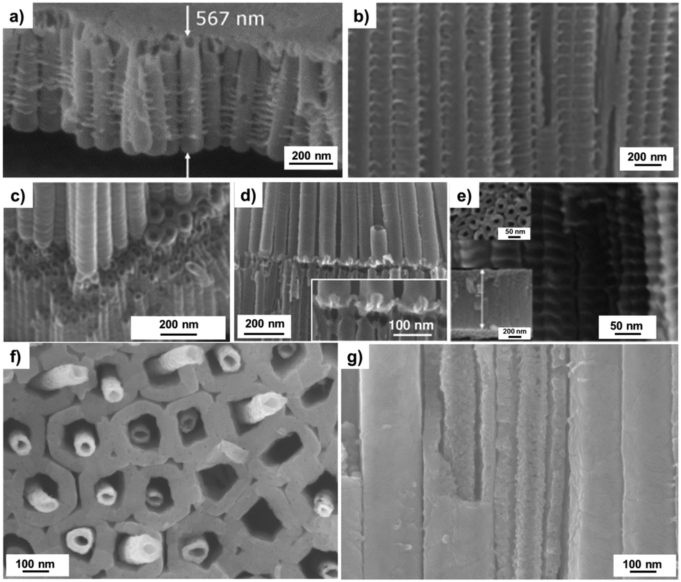 | ||
| Fig. 5 SEM images of: (a) TiO2 nanotubes with a rippled-wall morphology, (b) bamboo-type tubes, (c) branched-tubes, (d) inter-tubes, (e) TiO2 and Ta2O5 superlattice tubular oxide. (f and g) Top and cross sectional views, respectively, of tubes-in-tubes. (a) Reproduced with permission from ref. 142. (b and c) Reproduced with permission from ref. 57. (d) Reproduced with permission from ref. 58. (f and g) Reproduced with permission from ref. 135. | ||
Bamboo-type tubes,142,143 branched and inter-tubes,57,58,147 as well as tube stacks81,83,141,148 can be grown by a stop and continuation of the anodization, or pulsing the voltage during anodizing. By using appropriate alternating voltage cycling, a morphology that resembles bamboo is formed (Fig. 5b). With this approach, oxide that connects tubes at their bottom is grown at each voltage step and by using different anodization durations the distance between the stratification layers can be adjusted.56 By reducing the voltage to distinct lower voltage,57,58 also branched tubes can be grown with distinct lower tube diameters. Depending on the anodization conditions, the second tube layer is either grown through the bottom of the first layer (Fig. 5c)57 or in the gaps between the existing tubes of the upper layer, that is, inter-tubes are formed (Fig. 5d).58,147 Heteromaterial superlattices can be produced using sputter-deposited multilayer metal stacks as substrate for anodization – this has been shown for alternating metal layers (e.g., Ti–Ta, Ti–Nb, Ti–Zr).81,83,148 Key is that experimental conditions can be established that lead for both elements to a self-organized tubular nanostructure (Fig. 5e). Given the large number of materials for which self-organized oxide nanostructures can be grown, this technique can produce a wide palette of multilayered nanostructures. A peculiar morphology are tube-in-tube structures as shown in Fig. 5f and g that can be regarded as a special case of double-walled nanotubes as discussed below. More detailed descriptions of different tube morphologies can also be found in ref. 27, 28, 52, 57, 103, 149.
4. Double- vs. single-walled
An important aspect of tube growth that is widely neglected or overlooked in literature is the self-induced double-layered, or double-walled, morphology of anodic oxide nanotubes grown in many organic electrolytes, which for several applications is detrimental. We will discuss, in the following, the origin of these double-walled tubes (Fig. 6a–d) and ways to produce single-walled tubes (Fig. 6e and f) of a much higher oxide quality.53–55,146,150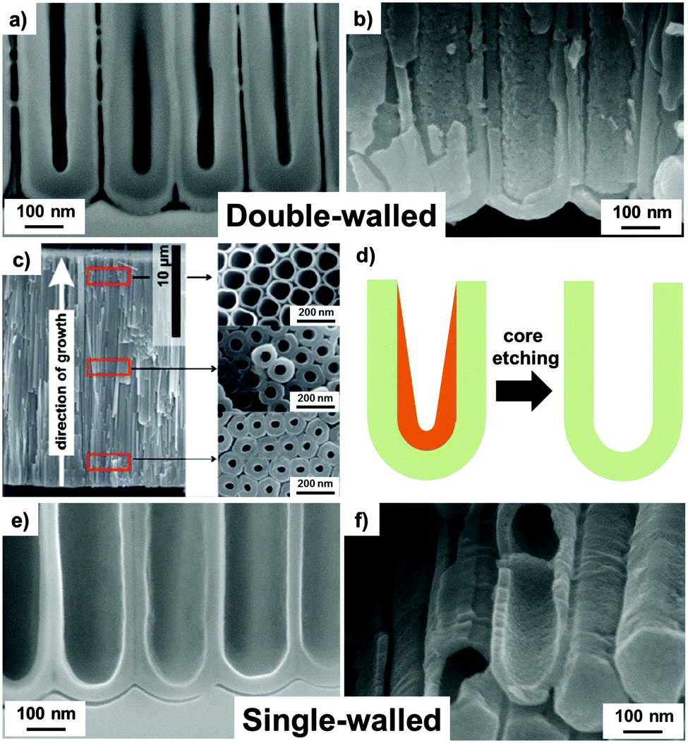 | ||
| Fig. 6 Cross-sectional SEM images of ion-milled (a) “as formed” and (b) annealed tubes (showing the typical double-walled morphology). (c) Full cross-sectional SEM image of a double-walled TiO2 nanotube layer (formed in EG-based electrolyte) with top-view SEM images taken at the top, from the fractures in the middle, and close to the bottom of a tube layer. (d) Schematic drawing of inner layer removal through chemical etching with a 1:3 solution mixture of H2O2/H2SO4 for 6 min at 70 °C. (e and f) Single-walled tubes after core removal process leaving behind only the outer tube shell. (a, b and d–f) Reproduced from ref. 146 with permission from the Royal Society of Chemistry. (c) Reproduced from ref. 55 with permission from the Royal Society of Chemistry. | ||
The most widely used electrolytes to grow ordered and seemingly well-defined TiO2 nanotubes are based on ethylene glycol, water and fluorides. While these tubes in top or side view SEM appear uniform, a close look at ion milled cross sections in SEM (Fig. 6a and b) or tubes in TEM (particularly at the lower tube end), reveals that the walls of these TiO2 nanotubes consist of two different types of oxide, namely an outer shell (OS) and an inner shell (IS), as also illustrated in Fig. 3c. The two-shell nature becomes even more apparent when the tubes are annealed to crystallize their tube walls. If the annealing temperature is sufficiently high and/or for a more rapid annealing than ∼10 °C min−1, a clear separation between inner and outer shells can no longer be observed as IS and OS sinter together (maintaining the lower quality oxide characteristics).53–55,151 As discussed in more detail in Section 7, this can be a critical factor in affecting not only the geometry but also the properties of TiO2 nanotube layers. Detailed investigations showed that the as-grown outer shell consists of comparably pure TiO2, while the inner layer is composed of carbon-rich titanium oxide or oxy-hydroxide.53,55,146,152 To a large extent, this TiOxHyCz layer stems from precipitated Ti-ions, ejected from the oxide but not solvatized as TiF62−, combined with carbon species embedded from the electrolyte during the anodization process. This inner layer typically dictates the inner tube morphology as it narrows the inner diameter of the tubes and limits the possibilities of a uniform and functional coating of the inner tube wall.53–55 This inner layer is more sensitive to etching in the fluoride-containing electrolyte, compared with the outer shell TiO2. This results in a V-shaped inner tube morphology (Fig. 3c), while OS preserves a nearly constant thickness along the whole tube length. For tubes grown for some time, a proper evaluation of double wall formation can therefore only be done close to the bottom of the tubes, where the thickness of IS is still maintained (Fig. 6c). The type of electrolyte used has a strong impact on whether or not, or to what extent, an inner contamination shell is formed. As mentioned, the most frequently adopted ethylene glycol (EG)/H2O mixtures that contain NH4F or HF lead to double-walled nanotubes, whereas dimethyl sulfoxide (DMSO) or EG/DMSO mixtures can be applied to grow single-walled tubes. This effect can be ascribed to different reactions of the electrode (anode) with the adjacent electrolyte (DMSO vs. EG) during anodization. High anodic voltages cause Schottky barrier breakdown in the oxide, which generates valence band holes that, similarly to photocatalysis, can react with the environment, either directly with electrolyte species or with H2O, and form OH˙ radicals.55,153 A range of carbonaceous oxidation products can be produced that adsorb on TiO2 and are incorporated in the OS. In contrast to EG, DMSO is capable of capturing radicals nearly 10-times faster154 and the reaction products are solvatized in the electrolyte while, in the case of EG, they are incorporated in the IS.54,55 More recent reports introduced an even more widely useful technique for fabricating single-walled TiO2 nanotubes. It was found that for essentially all double-layered TiO2 nanotubes, the IS can be selectively etched leaving behind the OS, as an intact single wall, by exposing the samples to a piranha solution under optimized etching conditions, as shown in Fig. 6d–f.146 This has been demonstrated recently in detail for tubes grown from EG electrolytes containing NH4F, and lactic acid, LA (here, LA acts as an additive that allows for an unprecedented ultrafast growth of ordered TiO2 nanotubes due to a field supporting effect).150 Noteworthy, the IS-removal process can be carried out successfully over the entire nanotubular layer, for a wide range of tube lengths i.e., from 2.5 μm up to 16 μm as reported in ref. 146 and 152.
A more detailed comparison of the composition of double-walled and single-walled tubes produced by selective etching of IS has been obtained by means of Thermo-Gravimetric Analysis, coupled with Mass Spectrometry (TGA-MS) – characteristic decomposition patterns are shown in Fig. 7a and b. It is apparent that ∼2–3 wt% loss occurs in both layers, owing to water desorption (notably, the desorption of physically adsorbed water occurs at ∼180–200 °C, due to the presence of hydroxyl groups that interact with uncoordinated surface atoms).155 In contrast, a clear difference in CO2 release signals can be observed: CO2 evolution in single-walled tubes produces a relatively low weight loss (∼5 wt%) that can be reasonably explained with the pyrolysis of environmental contaminants that are adsorbed on TiO2 surface,54 while remarkably higher amount of carbon is released as CO2(g) if double-walled tubes are heated up to ∼350–400 °C. This is ascribed to a thermal oxidation of the carbon species in the inner shell of the tubes.135
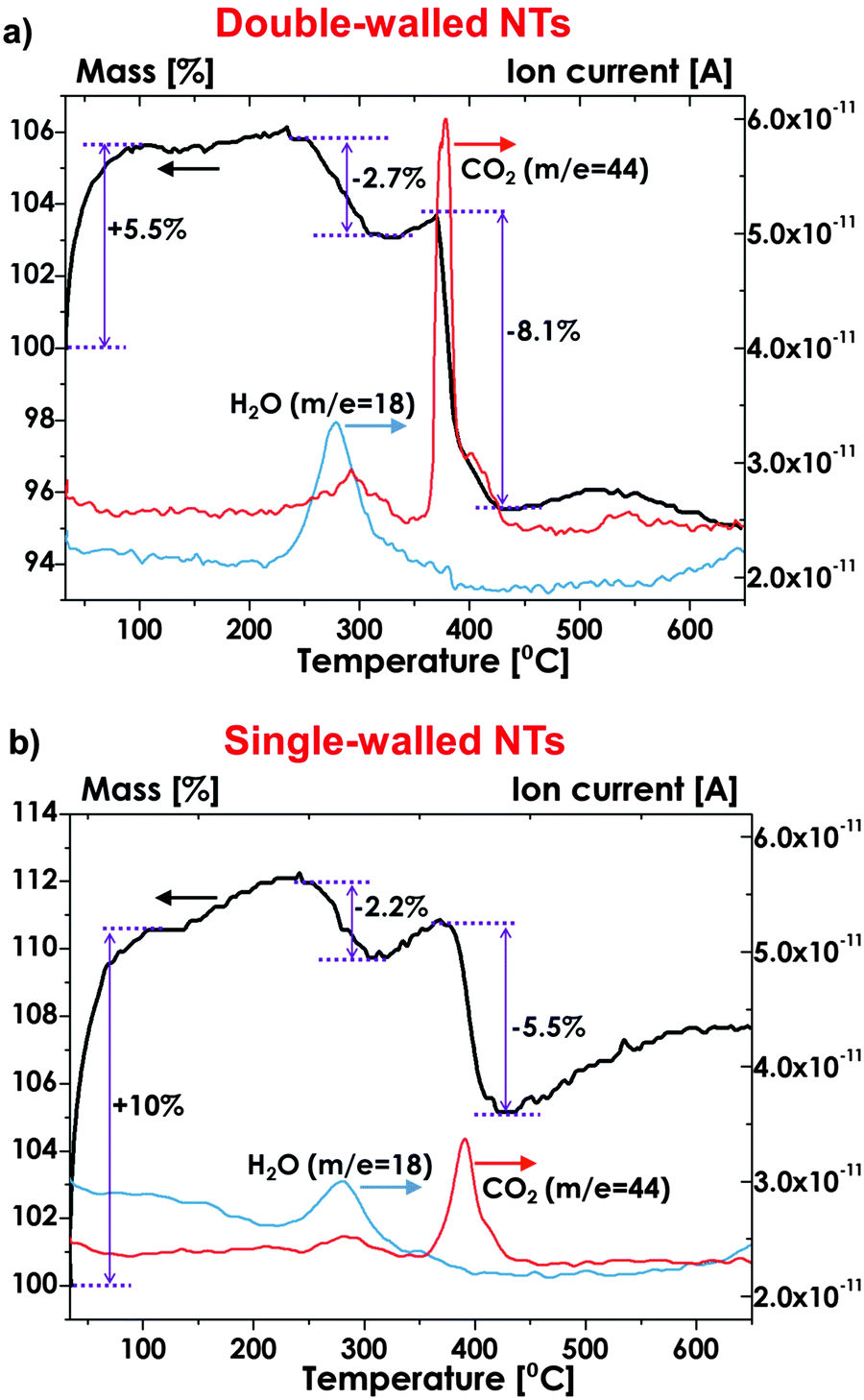 | ||
| Fig. 7 Thermal desorption profile for m/z− = 18 (H2O) and for m/z− = 44 (CO2) measured by Thermo-Gravimetric Analysis coupled with Mass Spectrometry (TGA-MS) for (a) double-walled and (b) single-walled tubes. (a and b) Reproduced with permission from ref. 135. | ||
Finally, the recently reported tube-in-tube morphology (Fig. 5f and g) is an unusual arrangement obtained under conditions similar to that for ultra-fast growth of double-walled TiO2 nanotubes.150 Though more detailed investigations are required, the formation of this unconventional morphology is ascribed to the low temperature adopted during the anodization process that both limits the tube growth speed and enables a particularly slow fluoride-etching of C-rich layers.135
5. Towards maximized ordering and ideal arrangements
Systematic experimental investigations of growth parameters led over the years to a remarkably improved control over the morphology of the tubes, as well as of the degree of self-organization. While the historically first used water-based electrolytes yield nanotube layers with a relatively poor degree of self-ordering,47–50,52 today a variety of electrolytes and conditions112,156,157 can provide virtually ideal hexagonal-order over long surface ranges – but typically ideal order is limited to the size of an individual Ti crystal grain.158 For TiO2 nanotubes, strategies that can provide an extended degree of self-organization have been adopted from approaches developed for ordered porous alumina, e.g., the use of pure and large-grain substrates that reduce the detrimental effect of substrate contaminants, inclusions and grain boundaries on the degree of ordering.159 A most facile fabrication technique for improved order is double-anodization. This multiple-anodization technique was introduced by Masuda et al. for anodic Al2O3.41 The concept is based on the fact that the degree of self-organization in anodic layers is improved as the tubes grow, and gradually increases towards their bottom (misfitting tubes are eliminated). Therefore, if a first grown sacrificial nanotube layer is removed from the metallic substrate, hexagonally ordered footprints (dimples) are left behind that serve as pretextured initiation sites for the following anodization (Fig. 8a). The so-fabricated tubes feature a more regular hexagonal shape (thus, the standard deviation in the tube diameter is narrowed), and the number of defects is strongly decreased (Fig. 8b and c).156,160–162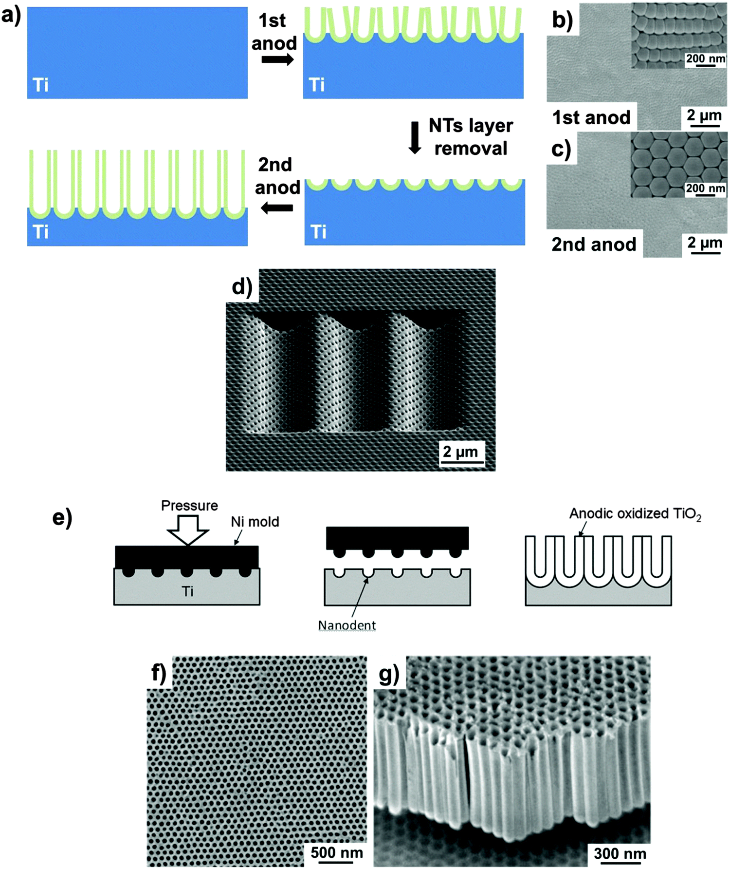 | ||
| Fig. 8 (a) Schematic of the fabrication of TiO2 nanotubes by a double-anodization approach. SEM bottom views of ordered domains of TiO2 NTs after the 1st (b) and 2nd (c) anodization. (d) SEM image of TiO2 nanotubes grown by FIB-guided anodization on a concave pattern. (e) Schematic diagram of the fabrication of an ideally ordered anodic TiO2 layer on a Ti foil pretextured through nanoindentation. (f and g) Typical SEM micrographs of long-range ordered anodic titania nanotubes grown on a nanoindented Ti metal substrate. (b and c) Reproduced with permission from ref. 160. (d) Reproduced with permission from ref. 166. (e–g) Reproduced with permission from ref. 171. | ||
However, long-range ordering, with a narrowly dispersed pore diameter distribution and a domain size larger than substrate grains, is fundamental for some emerging applications such as photonic crystals and high density magnetic storage media.44,163,164 Strategies that can induce long-range surface pretexturing are mold imprinting or focused-ion-beam (FIB) surface nanopatterning. FIB-induced surface pretexturing165 offers the possibility of producing ordered concave arrays as initiation sites for anodization, with uniform and controllable depth, that enables the fabrication of TiO2 nanotubes with different patterns with square, triangular and flower-like cell shapes, also with accurate control on inter-tube distance (Fig. 8d).166–168 Nevertheless, FIB patterning (pixel after pixel) is a time-consuming sequential writing process and thus inadequate for patterning of large areas of a Ti metal substrate. It may be noteworthy that mask-based, and thus parallel ion beam patterning processes have been proposed, but these still are widely unexplored.169
A straightforward parallel process to create initiation sites that keep the registry across Ti metal grains is nanoimprinting the Ti surface with an ordered array of convexes using a metal mold (Fig. 8e–g). In this case, the mold is produced using e-beam lithography. The advantage of this technique is that the mold can be used repeatedly, and spacing and patterns are adjustable by the lithography process that produces the mold. Most inhomogeneity typically observed under non-guided self-organizing anodization (such as initiation layers and the grain-dependent orientation dictated by the polycrystallinity of metallic substrates) is also largely eliminated. However, given the high Young’s modulus of Ti (116 GPa), only molds of very hard materials can be adopted.170,171
6. Advantages of lifted-off TiO2 nanotube layers
The defined geometry of nanotubes and the possibility of controlling their length and diameter make anodic tubes particularly suitable for membrane-type applications that additionally exploit TiO2 functional features, such as flow-through microreactors for photocatalysis and dye-sensitized solar cells.145,146,151,172–175 For solar cells, not only the ease of electrolyte access in a two side open membrane (Fig. 9a) is of advantage, but even more beneficial are the superior electronic properties (lower electrical resistance) provided by bottomless tubes.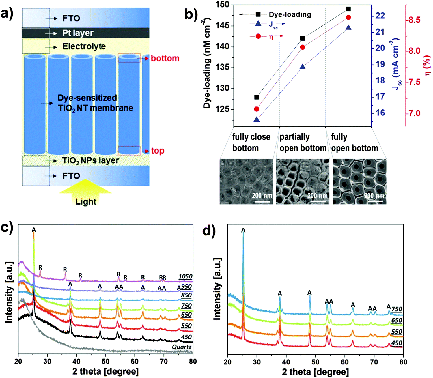 | ||
| Fig. 9 (a) Sketch of anodic TiO2 nanotube-based front-side illuminated DSSC. TiO2 tube arrays are detached from Ti substrates, bottom-opened, and transferred onto FTO slides in a tube-top-down configuration. (b) Dye loading, short-circuit current, and power-conversion efficiency of DSSCs fabricated from tube membranes transferred onto FTO glass in a tube-top-down configuration. The SEM images show a close view of the different degrees of tube bottom opening. Reproduced with permission from ref. 172. (c and d) XRD patterns of membranes annealed at different temperatures and under different atmospheres: (c) 450–1050 °C in air; (d) 450–750 °C in O2 (the patterns were collected after transferring the annealed membranes on quartz glass slides). Reproduced with permission from ref. 175. | ||
Nanotube membranes are produced by separating the anodic tube layer from the metallic substrate, followed by tube bottom opening. Albu et al. reported the first self-organized, free-standing TiO2 nanotube membrane prepared by selectively dissolving the Ti substrate with a metal etching treatment in a CH3OH/Br2 solution. After substrate dissolution, the tubes were still closed; thus exposing the layer to HF vapors was necessary in order to open the bottom.145 Afterwards, a range of different approaches were reported for both lift-off and opening procedures, such as chemical etching, sonication, and voltage alteration.176–178 The main challenge encountered when separating nanotubes from the substrate is due to the relative brittleness of the anodic layer, particularly if the membrane is thinner than 50 μm or when large membrane areas are desired. Also, bottom removal mainly by HF, oxalic acid, H2O2 or other etchants has to be carefully controlled.
More reliable approaches have recently been developed that allow the detachment of TiO2 nanotube layers from the Ti metal substrate to form self-standing membranes as thin as ∼2 μm.151,172,174,179–181 Here an anodization–annealing–2nd anodization sequence is employed: following the first anodization step, the nanotube layers are annealed in air at a comparably low temperature, i.e., 150–300 °C (to make the tubes water-free and partially crystalline); then the second anodization is carried out to produce a thin underlayer of amorphous TiO2 NTs. This second amorphous layer can then be selectively dissolved by a treatment in HF or H2O2 solutions. Due to the much lower etching rate of the annealed layer, the amorphous tubes are selectively dissolved and free-standing membranes can be produced that are defect-free over the entire surface area.175 Noteworthy, only when the lift-off process is performed in H2O2, tube bottom opening is simultaneously achieved.172 Alternatively, the first layer can be produced from a double anodized layer156,160–162 that then is annealed and chemically undermined. This treatment has been applied to self-standing and stable TiO2 NTs membranes of ∼1.8–50 μm thickness.181
A unique possibility offered by bottomless TiO2 NT membranes is the fabrication of size-selective flow-through microreactors that can be used for virtually any photocatalytic reaction (e.g., pollutant degradation and membrane de-clogging in protein separation).145,175,182 For example, if a tube membrane is used to separate two (differently filled) compartments of a flow-through reactor, a concentration gradient is created that governs the solution diffusion until an equilibrium is reached. Interestingly, if the surface of the membrane is illuminated, photocatalysis (and membrane de-clogging that is particularly useful for re-opening of the membrane channels)182 can be activated that, by permanently degrading the arriving reactant molecules, contributes to accelerate the solution diffusion.145,175
Recently, also considerable benefits of using lift-off membranes as anodes for dye-sensitized solar cells (DSSCs) have been reported. To construct photo-anodes such membrane layers are, either with151,174 or without172,173 bottom, glued to a conducting glass surface typically using TiO2 nanoparticle suspensions. These arrangements have several advantages: not only the photo-anodes provide the classic advantage of 1D-nanostructures, namely the one-dimensional transport, but additionally if the anodic TiO2 NT layer is detached from the Ti substrate and transferred onto FTO, the photo-anode can be irradiated through the FTO glass in a “front-side” illumination configuration (Fig. 9a). With this geometry, the DSSC reaches higher efficiency as the light losses typically observed in a back-side application due to light absorption in the electrolyte and by the Pt counter electrode are minimized.151,172,174,183 Moreover, the solar cell efficiency is significantly enhanced for bottom-opened tube membranes (Fig. 9b).172 This has been ascribed to a higher electron mobility within the tube layer, owing to the absence of the high-resistivity tube bottom, and to an optimal electrolyte percolation through the dye-sensitized fully-open tube scaffold. This in turn minimizes charge recombination as, upon electron injection into TiO2, the dye can readily react with the electrolyte in its vicinity; even more, when a bottomless tube configuration is adopted, the ability of the dye solution to penetrate the entire TiO2 structure is significantly enhanced; this also implies that an open-bottom morphology allows for optimal dye-loading.
It should also be mentioned that the detachment of tubes from the metal prevents the formation of rutile at the metal/oxide interface during annealing (rutile is formed by thermal oxidation of Ti metal). Rutile is detrimental for TiO2 in photo-electrochemical applications due to the poor electronic properties compared with anatase.184–186 It is well established that direct annealing of metallic Ti in air at temperatures above 450 °C leads to a relatively thick rutile layer – this also occurs with the metal underneath the tubes. If the metal layer is absent, as in detached membranes, no rutile is detected up to annealing temperature of 950 °C (Fig. 9c and d).174,175 Although no remarkable difference in the phase composition of TiO2 membranes annealed up to such a high temperature can be observed, it is evident that a gradual increase in the crystallinity degree, that is, a more intense main anatase reflection (at 2θ ∼ 25.3°), is obtained when increasing the annealing temperature up to 650 °C.175 This in turn enhances the charge transport properties of the layer as electron transport in the tubes becomes considerably faster (this is advantageous for maximizing charge collection at the oxide/electrode interface in DSSC).174 Finally, also annealing in O2 produces fully anatase TiO2 membranes up to 750 °C (that is, no rutile is detected), if the nanotube layers are detached from the Ti metallic substrate. As discussed below, O2-annealing, for instance, is particularly useful to fill native oxygen vacancies in TiO2 and, hence, produces a “higher quality” oxide, with optimized conductivity.187
7. Tube morphology and optical and electronic properties
Most relevant applications of TiO2 nanotube layers ensue from the beneficial combination of the material’s intrinsic properties with the one-dimensional nanoscale geometry. A key point is that this geometry can in principle provide a directional (i.e., faster) charge transport through the oxide. In any form of TiO2, another factor that strongly affects the electronic properties is the crystal structure of the material. In its amorphous form (such as in as-grown tubes), TiO2 has a mobility gap of 3.2–3.5 eV and a very low electron mobility. Upon crystallization to anatase or rutile (typically achieved under air annealing conditions) an indirect optical band gap of 3.2 eV and 3.0 eV is obtained, respectively.188 Both polymorphs show a higher mobility than amorphous TiO2 but, in particular, a crystallization into anatase is often reported to be crucial to obtain a high electron mobility.189,190 Optical and electronic properties of TiO2 are largely influenced by oxygen vacancies and Ti3+ states in the lattice, that is, electrons may be trapped in the Ti3+ states or holes in the oxygen vacancies and injected in the nearby conduction and valence bands by thermal excitation. The conductivity of TiO2 is dominated by Ti3+ trap states and, in the polycrystalline material, also by grain size. Therefore, a variation in the annealing conditions of TiO2 nanotubes (such as temperature, time, and atmosphere) can alter the layer resistance (and the electron mobility) over several orders of magnitude.191,192As previously pointed out, annealing of TiO2 on the metal substrate (Ti) strongly differs from annealing free-standing membranes. In both cases, upon increasing the annealing temperature (i.e., 250–500 °C) a significant decrease in the tube resistivity can be obtained, owing to amorphous layers being converted to crystalline anatase. However, for TiO2 nanotubes on the Ti substrate, annealing as described above may cause rutile formation due to the thermal oxidation of the metal substrate. As a negative consequence (in view of photo-electrochemical applications), the overall resistivity of these tube layers rises again (Fig. 10a).193 In contrast, free-standing membranes can be annealed up to ∼1000 °C while maintaining a pure anatase phase – rutile is not formed owing to the absence of the Ti metal substrate (Fig. 9c and d), and such layers show clearly improved electronic properties.151,174,175,187
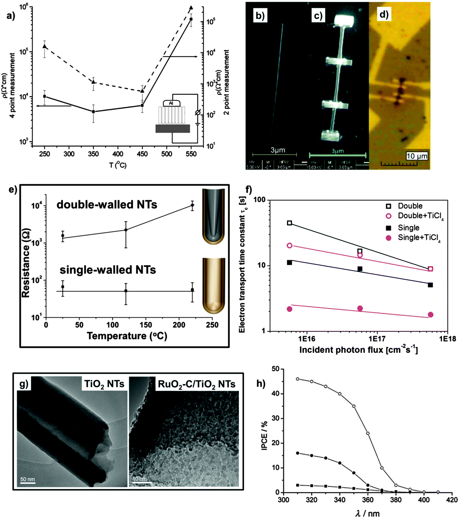 | ||
| Fig. 10 (a) Comparison of specific resistivity values of TiO2 nanotubes vs. annealing temperature obtained by 4-point (left axis) and 2-point (right axis) measurements. Reproduced with permission from ref. 193. (b–d) Procedure of four-point conductivity measurement with a single nanotube: (b) single TiO2 nanotube before fixing it on the substrate, (c) the nanotube fixed with WCx, and (d) after producing the electrical contacts. Reproduced with permission from ref. 194. (e) Comparison of electrical resistance of the single-walled and double-walled nanotube layers measured at different temperatures. Reproduced from ref. 54 with permission from the Royal Society of Chemistry. (f) Electron transfer time (τc) constants obtained from IMPS measurements performed under UV light irradiation (325 nm) for double-walled (double) and single-walled (single) TiO2 nanotubes, also modified with a layer of TiCl4 nanoparticles (double + T1 and single + T1, respectively). Reproduced from ref. 146 with permission from the Royal Society of Chemistry. (g) TEM micrographs of bare TiO2 NTs before annealing (left-side) and of carbon-cladded TiO2 NTs modified with the deposition of RuO2 nanoparticles (right-side). Reproduced from ref. 199 with permission from the Royal Society of Chemistry. (h) Incident Photon-to-Current Efficiency (IPCE) spectra of different C-contaminated TiO2 nanotube layers that show sub-band gap response: (■) amorphous NTs, (●) NTs annealed in air, (○) NTs annealed in CH3OH-containing atmosphere. Reprinted with permission from J. Electrochem. Soc., 2010, 157(3), G76. Copyright 2010, The Electrochemical Society. | ||
Typical resistivity values in the range of 104–105 Ω cm193 are obtained (from both four- and two-point measurements) for anatase tube layers anchored on the metal substrate – four-point measurements may however better reflect the resistivity dependence on the annealing temperature. However, two- and even four-point measurements carried out with metal contacts on the tubes, but the metal substrate underneath, are somewhat ambiguous. Most informative are four-point techniques applied to a single TiO2 nanotube (Fig. 10b–d).194 A crucial finding is that the conductivity measurements in this case show orders of magnitude higher values than measurements on the substrate. This large difference cannot be ascribed to the presence of the rutile underlayer but rather reflects an high resistivity of the tube bottoms (this explains why bottom-opened tubes lead to significantly higher solar conversion efficiencies when used in DSSCs, Fig. 9b). Moreover, the T-dependence of resistance for a single tube was found compatible with a Mott variable range hopping mechanism, that is, conductivity is provided by electron hopping within localized states in a mobility gap.194,195 In other words, these measurements indicate that not grain boundaries (crystal size) in the tube wall are limiting the conductivity, but the intrinsic defect states within TiO2 crystals forming the nanotubes. While these measurements on single tubes are most informative, many data were obtained using a Ti/TiO2/metal top contact two-point measurement – simply due to the facility of this approach. In spite of all the shortcomings of two-point measurements, phenomena such as water loss, anatase/rutile formation and defect-elimination by pure oxygen annealing can be detected and are in line with expectations.193,196,197
Using this two-point approach, the effect of the inner C-rich layer on conductivity was also investigated, by comparing double-walled and single-walled NTs.54 A clear difference in the conductivity can be already observed with as-formed tubes, with the double-layered exhibiting a somewhat lower resistance. However, after annealing, a drastic increase (about 10–100 times) in the conductivity properties is obtained for the single-walled tubes while a resistivity increase is observed for the double-walled tubes (Fig. 10e). Most likely the trend observed for double-walled tubes is due to the high amount of residual water that remains entrapped in the tubes up to ∼180–200 °C, as evident from TGA-MS results and, even more, can be ascribed to the high C-contamination content that originates from the IS layer (Fig. 7a);135 the enhanced electrical conductivity of single-walled tubes therefore indicate that removal of the inner contamination layer leads to beneficial electrical properties in the tubes after crystallization (single-walled tubes show a pure (no contamination) and large crystalline TiO2 structure, whereas in double-walled tubes contamination is still present and a typically smaller TiO2 grain size within the tube wall is observed).135 Nevertheless, even better electron transport properties can be achieved exposing single-walled tubes to a TiCl4 treatment. Not only the tube walls become then decorated with a nanoparticle layer, but the treatment seems also able to passivate defect states, leading to clearly faster electron transport (Fig. 10f).146,198
However, the C-contaminated IS of double-walled tubes has also been used to create beneficial effects when annealing EG-based tubes under inert gas conditions. A thin carbon layer can be formed that uniformly coats the inner walls of TiO2 NTs.54,55,150,199 Such a cladding with a graphitic-like layer leads to enhanced conductivity, and provides a path to attach additional functionalities to the tubes, as the entire chemistry for modifying carbon-based layers becomes accessible200,201 and applicable to TiO2 NTs. This strategy can serve for example to fabricate scaffolds for anchoring a thin layer of RuO2 nanoparticles (i.e., a standard material for supercapacitors, Fig. 10g), and considerable performances of TiO2 NTs as supercapacitor device can be obtained.199
Photo-electrochemistry and, in particular, Incident Photon-to-Current Efficiency (IPCE) measurements (i.e., the photocurrent collected per incident photon flux as a function of illumination wavelength) are generally employed to investigate the optical properties of a semiconductor material, provide quantitative information on its band-gap and evidence true charge conduction at the corresponding wavelength (this in contrast to light absorption measurements).202 Typically, the main mechanism of light absorption in semiconductors is due to inter-band electron transitions. While a number of physical properties may be altered in small nanocrystals,203,204 in TiO2, optical quantum confinement and band-gap widening (that is, a measured Eg of ∼3.8 eV) can be practically observed only in tube walls or nanosheets that are prepared through hydrothermal procedures (that is, in “real nanotubes”) as they feature a wall thickness in the range of atomic sheets,20 while in general nanotubes grown by electrochemical anodization, having a wall thickness typically larger than ∼5 nm, show a band-gap corresponding to that of the bulk material (i.e., Eg ∼3.0–3.2 eV). As TiO2 is an indirect band-gap semiconductor, electronic transitions are phonon-coupled and, for size ranges <20 nm, phonon confinement effects can be observed and identified from TiO2 Raman peak widening and shift. For instance, in TiO2/Ta2O5 superlattice nanotube structure, TiO2 size units are confined to ∼10 nm in two dimensions and typical blue-shift and significant broadening of anatase peak in Raman spectra, as compared to the reference TiO2 material, have been reported.148
Typically, for anodic titania nanotubes, two factors play major role in the light absorption and in affecting photo-induced electrochemistry: (i) a contribution to the photoresponse from tube walls is observed only if NTs are crystalline, (ii) upon annealing, the donor concentration in nanotubes is usually very high (1018–1019 cm−3), i.e., two orders of magnitude higher than for conventional TiO2 nanoparticles.205 Although, compared to nanoparticles, tubes feature more inter-band trap states (e.g., oxygen vacancies) charge carrier transport in NTs is faster than in a nanoparticulate film.192 Electron diffusion lengths reported for nanotubes are 30 times longer than in nanoparticles, particularly under low-intensity irradiation.102
In view of these considerations, another promising way to improve electron transport in TiO2, and hence its performance in photo-electrochemical applications (e.g., DSSCs and photocatalysis), and to extend its light absorption spectrum in view of enabling visible-light photoactivity, is to introduce a dopant (that is, suitable inter-band states) into the TiO2 lattice. The dopant can either be a non-metal or a transition metal cation. In the latter case, metal cations, e.g. Ta and Nb, usually replace Ti in the TiO2 lattice and promote electron conductivity in the NT layer.77,85 For non-metal doping, most frequently investigated are N,206 C,207 S,208 and P209 that either replace O-atoms in the TiO2 structure (substitutional doping) or are stacked in interstitial spaces (interstitial doping), and generate suitable states in the band-gap and increase the conductivity of TiO2 nanotubes (low dopant concentration) or lead to band-gap narrowing (high dopant concentration).
Different approaches are reported to prepare doped TiO2 nanostructures, among which thermal treatment in a suitable gas atmosphere, e.g. NH3, is mostly adopted. Although findings of C-doping in TiO226–28,210,211 are to a certain extent ambiguous,202 C-containing tubes (that is, tubes with a double-walled morphology where carbon-uptake is due to the decomposition of the anodizing organic electrolyte under applied voltage) exhibit a change in the TiO2 optical properties. Light absorption and photocurrent spectra taken for tubes and membranes show that carbon contaminants (∼3 at%) lead to a sub-band gap response (Fig. 10h). Also, the conversion of TiO2 nanotubes to semimetallic TiOxCy, by thermal treatment in an acetylene atmosphere, or to TiN nanotubes, by a high temperature treatment in NH3, drastically changes the electronic properties of the starting material to a semimetallic nature and also improves its mechanical stability.212,213 Most recently, high pressure hydrogenation214 as well as high-energy proton215 and low-dose nitrogen216 implantation into TiO2 tube layers have been reported to alter not only the electronic structures of TiO2, but also to create catalytically active surface sites for improving the photocatalytic H2 evolution of TiO2 NTs.
Finally, a most unique possibility offered by anodic TiO2 nanotubes is the doping of tubes with a certain metal X, using suitable Ti–X alloys as metallic substrate for electrochemical anodization, where the alloyed species gets incorporated into the oxide. A number of reports show doping of tubes with Cr,87 V,78 W,37 Ta84–86 and Nb.77,79,80,82,217 In particular, in optimally doped and annealed TiO2 tubes, both Nb and Ta act as electron donors and hence increase the electron conductivity of the NT layers. This was e.g. demonstrated for nanotube arrays doped with small amounts (up to 0.1 at%) of Nb79,80,217 or Ta,85,86 for which a significantly enhanced performance in photo-electrochemical water splitting and dye-sensitized solar cells was observed. Other outstanding features, remarkable for nanotube application in electrochromic devices and ion intercalation based batteries, that can be obtained by anodizing Ti–X alloys are a higher optical contrast and a higher structural cycling stability for reversible Li-intercalation processes compared to pure TiO2 nanotubes. Particularly interesting is the case of superlattice NTs grown from sputter-deposited multilayer metal stacks of e.g. Ti-Nb that, due to the small size of the alternating TiO2/Nb2O5 segments (less than 10 nm), showed clearly less mechanical rupture by stress-induced burst.81 A superior mechanical stability has also been reported for TiO2 nanotubes grown in the presence of lactic acid in the electrolyte. TiO2 NTs grown under these specific conditions could be exposed to a more than three-time larger external force in tensile tests, compared to conventional tubes, before mechanical failure (cracking) of the tubes occurred.218 This characteristic makes LA tubes particularly interesting for robust membranes, with the single tubes maintaining their integrity during the membrane fabrication process.
In contrast to previous Ti–X alloy examples (where X is typically a non-noble metal), anodization of noble metal alloys of Ti lead to noble metal nanoparticle-decorated tubes,90,91,219i.e., noble metals, such as Au and Pt, are not oxidized during the anodization process. With this approach, the decoration density of Au or Pt nanoparticles can be easily controlled by the amount of the noble metal in the alloy and by the anodization time. This tuning of nanoparticle interspacing is in turn particularly useful for obtaining an optimal (photo)catalytic activity, such as in the splitting of water or as chemo-selective catalytic sites.90,91
All these examples illustrate that for anodic TiO2 NTs outstanding knowledge and control over a large set of inherent physico-chemical properties has been acquired within the last decade of research. These findings provide key strategies to tailor the characteristics of TiO2 NTs, e.g., their morphology, light absorption, conductivity, electron–hole mobility, etc. in a synergistic manner, in order to provide versatile platforms for various remarkable functional applications, such as photocatalytic and photo-electrochemical water splitting (H2 generation), DSSCs, and size-selective microreactors for photocatalytic and biochemical reactions.27,28,90,145,146,182,215,216
8. Conclusion
Titanium dioxide is by far among the most investigated functional metal oxide. This is due to the set of specific properties (e.g., non-toxicity, corrosion resistance, relatively long electron diffusion length, and biocompatibility) that makes TiO2 attractive for various applications including photocatalysis, photo-electrochemistry, and biochemistry. The possibility of growing porous anodic nanostructures and, in particular, self-organized and highly-aligned TiO2 nanotubes through electrochemical anodization has further increased the research interest on titania due to inherent advantages of tubular structures, such as large surface area, directional charge and ion transport properties, size exclusion effects, and defined diffusion behavior.The present review emphasizes critical aspects in the formation mechanism of self-ordered TiO2 nanotubes, and a wide range of morphology and property variations. We discuss the current understanding of the key factors that drive self-organization and attempt to show features common to ordered anodic nanoporous structures, such as porous Al2O3 and ordered TiO2 nanotubes. In spite of common principles underlying their growth, there are crucial differences not only in terms of alumina and titania anodic nanostructure morphologies, but also the influence of various electrochemical growth parameters, that have been shown to strongly affect the morphology, composition and structure of the resulting nanotube layers. With this review we try to highlight the importance of such variations and, at the same time, to provide guidelines for the selection of growth conditions specific for the intended use of the tube layers. We introduce most recent nanotube arrangements, such as stacks, bamboo-type tubes, branched and inter-tubes, tube-in-tube morphologies and, in particular, we point out key differences between single- and double-walled tubes along with their intrinsic properties. We give an overview of the optimized preparation and use of TiO2 tube membranes that in the recent few years have attracted strong interest in view of applications such as efficient DSSCs and size-selective flow-through photo-microreactors. Among most remarkable advantages of free-standing TiO2 membranes is certainly the possibility of establishing the desired pure anatase phase without conversion to rutile upon annealing TiO2 at high temperature. We discuss the most relevant electronic and optical properties of differently grown TiO2 nanotubes, giving a general overview on the approaches most frequently adopted to achieve desired modifications. Overall, we try to emphasize that anodic tubes are not simply tube-shaped TiO2 but there are a number of crucial (controllable) factors that can substantially affect their performance in application. Therefore, building on the expertise established up to now on TiO2 and on one-dimensional nanostructuring, one may identify some important future efforts. Improvements of synthetic strategies may not only ameliorate some intrinsic “weaknesses” of TiO2 (i.e., in optical and electronic properties, compatibility with bio-materials, ion-intercalation) but also address some of the current features of anodic nanotubes (i.e., crystallinity, degree of self-organization, control over tube morphology, length and diameter). Clearly, still a large potential exists for maximizing the performance of 1D TiO2 NT-based devices (e.g., adequate treatments to reduce the defects in NTs, or to intentionally create intrinsic defects that could affect light absorption and electron conductivity for higher efficiencies in photocatalysis and DSSCs-based applications; anodizing under specific conditions to adjust a desired material robustness for membrane and flow-through applications; improvement of the ordering and control of tube wall thickness to achieve electronic size effects) and for designing specific surface structures and chemistry. The last decade has shown that TiO2 nanotubes prepared through self-organizing anodization are nanostructured materials providing continuous surprises that trigger advances of nanotechnology and the development of energy-, environment- and bio-applications, owing to their intrinsic properties and to the versatility and scalability of the fabrication technique, and we hope this review provides some tools and strategies to facilitate further future achievement.
Acknowledgements
The authors would like to acknowledge the ERC, the DFG, and the DFG cluster of excellence “Engineering of Advanced Materials”, as well as DFG “funCOS” for financial support. Radek Zbořil (Regional Centre of Advanced Technologies and Materials, Olomouc, Czech Republic), and Manuela Killian, Marco Altomare, Anca Mazare, Ning Liu, Gihoon Cha, Jeong Eun Yoo and Xuemei Zhou are acknowledged for their valuable contributions.References
- C. M. Lieber, Solid State Commun., 1998, 107, 607–616 CrossRef CAS.
- C. Weisbuch and B. Vinter, Quantum Semiconductor Structures: Fundamentals and Applications, Amsterdam, 1991 Search PubMed.
- C. N. R. Rao, A. Muller and A. K. Cheetham, The Chemistry of Nanomaterials: Synthesis, Properties and Applications., Weinheim, Germany, 2004 Search PubMed.
- D. Khudhair, A. Bhatti, Y. Li, H. A. Hamedani, H. Garmestani, P. Hodgson and S. Nahavandi, Mater. Sci. Eng., C, 2016, 59, 1125–1142 CrossRef CAS PubMed.
- S. Iijima, Nature, 1991, 354, 56–58 CrossRef CAS.
- T. W. Ebbesen and P. M. Ajayan, Nature, 1992, 358, 220–222 CrossRef CAS.
- S. Iijima and T. Ichihashi, Nature, 1993, 363, 603–605 CrossRef CAS.
- D. T. Colbert, J. Zhang, S. M. McClure, P. Nikolaev, Z. Chen, J. H. Hafner, D. W. Owens, P. G. Kotula, C. B. Carter, J. H. Weaver, A. G. Rinzler and R. E. Smalley, Science, 1994, 266, 1218–1222 CAS.
- M. Bockrath, D. H. Cobden, P. L. McEuen, N. G. Chopra, A. Zettl, A. Thess and R. E. Smalley, Science, 1997, 275, 1922–1925 CrossRef CAS PubMed.
- J. C. Charlier and P. Lambin, Phys. Rev. B: Condens. Matter Mater. Phys., 1998, 57, 15037–15039 CrossRef.
- T. W. Odom, J.-L. Huang, P. Kim and C. M. Lieber, Nature, 1998, 391, 62–64 CrossRef CAS.
- J. W. G. Wildöer, L. C. Venema, A. G. Rinzler, R. E. Smalley and C. Dekker, Nature, 1998, 391, 59–62 CrossRef.
- M. E. Spahr, P. Stoschitzki-Bitterli, R. Nesper, O. Haas and P. Novák, J. Electrochem. Soc., 1999, 146, 2780–2783 CrossRef CAS.
- F. Krumeich, H. J. Muhr, M. Niederberger, F. Bieri, B. Schnyder and R. Nesper, J. Am. Chem. Soc., 1999, 121, 8324–8331 CrossRef CAS.
- M. Remškar, Z. Škraba, P. Stadelmann and F. Lévy, Adv. Mater., 2000, 12, 814–818 CrossRef.
- X. Sun and Y. Li, Chem. – Eur. J., 2003, 9, 2229–2238 CrossRef CAS PubMed.
- D. V. Bavykin, J. M. Friedrich and F. C. Walsh, Adv. Mater., 2006, 18, 2807–2824 CrossRef CAS.
- B. D. Yao, Y. F. Chan, X. Y. Zhang, W. F. Zhang, Z. Y. Yang and N. Wang, Appl. Phys. Lett., 2003, 82, 281–283 CrossRef CAS.
- C.-J. Jia, L.-D. Sun, Z.-G. Yan, L.-P. You, F. Luo, X.-D. Han, Y.-C. Pang, Z. Zhang and C.-H. Yan, Angew. Chem., Int. Ed., 2005, 44, 4328–4333 CrossRef CAS PubMed.
- T. Kasuga, M. Hiramatsu, A. Hoson, T. Sekino and K. Niihara, Langmuir, 1998, 14, 3160–3163 CrossRef CAS.
- W. Wang, O. K. Varghese, M. Paulose, C. A. Grimes, Q. Wang and E. C. Dickey, J. Mater. Res., 2004, 19, 417–422 CrossRef CAS.
- Y. Mao and S. S. Wong, J. Am. Chem. Soc., 2006, 128, 8217–8226 CrossRef CAS PubMed.
- P. Hoyer, Langmuir, 1996, 12, 1411–1413 CrossRef CAS.
- M. S. Sander, M. J. Côté, W. Gu, B. M. Kile and C. P. Tripp, Adv. Mater., 2004, 16, 2052–2057 CrossRef CAS.
- M. S. Sander and H. Gao, J. Am. Chem. Soc., 2005, 127, 12158–12159 CrossRef CAS PubMed.
- G. Wu, T. Nishikawa, B. Ohtani and A. Chen, Chem. Mater., 2007, 19, 4530–4537 CrossRef CAS.
- P. Roy, S. Berger and P. Schmuki, Angew. Chem., Int. Ed., 2011, 50, 2904–2939 CrossRef CAS PubMed.
- K. Lee, A. Mazare and P. Schmuki, Chem. Rev., 2014, 114, 9385–9454 CrossRef CAS PubMed.
- A. Ghicov, S. Aldabergenova, H. Tsuchyia and P. Schmuki, Angew. Chem., Int. Ed., 2006, 45, 6993–6996 CrossRef CAS PubMed.
- K. Yasuda and P. Schmuki, Electrochim. Acta, 2007, 52, 4053–4061 CrossRef CAS.
- H. Tsuchiya, S. Berger, J. M. Macak, A. Ghicov and P. Schmuki, Electrochem. Commun., 2007, 9, 2397–2402 CrossRef CAS.
- S. Berger, H. Tsuchiya and P. Schmuki, Chem. Mater., 2008, 3245–3247 CrossRef CAS.
- L. Liu, W. Lee, Z. Huang, R. Scholz and U. Gösele, Nanotechnology, 2008, 19, 335604 CrossRef CAS PubMed.
- H. Jha, R. Hahn and P. Schmuki, Electrochim. Acta, 2010, 55, 8883–8887 CrossRef CAS.
- K. Lee and P. Schmuki, Electrochem. Commun., 2011, 13, 542–545 CrossRef CAS.
- R. Ion, A. B. Stoian, C. Dumitriu, S. Grigorescu, A. Mazare, A. Cimpean, I. Demetrescu and P. Schmuki, Acta Biomater., 2015, 24, 370–377 CrossRef CAS PubMed.
- Y. C. Nah, N. K. Shrestha, D. Kim and P. Schmuki, J. Appl. Electrochem., 2013, 43, 9–13 CrossRef CAS.
- T. Rummel, Z. Phys., 1936, 99, 518–551 CrossRef CAS.
- W. Baumann, Z. Phys., 1936, 102, 59–66 CrossRef CAS.
- G. E. Thompson and G. C. Wood, Treatise on Materials Science and Technology, Academic Press, New York, 1983, pp. 205–329 Search PubMed.
- H. Masuda and K. Fukuda, Science, 1995, 268, 1466–1468 CAS.
- K. Uosaki, K. Okazaki and H. Kita, Anal. Chem., 1990, 62, 652–656 CrossRef CAS.
- C. R. Martin, Science, 1994, 266, 1961–1966 CAS.
- K. Nielsch, R. B. Wehrspohn, J. Barthel, J. Kirschner, U. Gösele, S. F. Fischer and H. Kronmüller, Appl. Phys. Lett., 2001, 79, 1360–1362 CrossRef CAS.
- M. Steinhart, Science, 2002, 296, 1997 CrossRef CAS PubMed.
- G. E. Thompson, Thin Solid Films, 1997, 297, 192–201 CrossRef CAS.
- M. Assefpour-Dezfuly, C. Vlachos and E. H. Andrews, J. Mater. Sci., 1984, 19, 3626–3639 CrossRef CAS.
- V. Zwilling, E. Darque-Ceretti, A. Boutry-Forveille, D. David, M. Y. Perrin and M. Aucouturier, Surf. Interface Anal., 1999, 27, 629–637 CrossRef CAS.
- D. Gong, C. a. Grimes, O. K. Varghese, W. Hu, R. S. Singh, Z. Chen and E. C. Dickey, J. Mater. Res., 2001, 16, 3331–3334 CrossRef CAS.
- R. Beranek, H. Hildebrand and P. Schmuki, Electrochem. Solid-State Lett., 2003, 6, B12–B14 CrossRef CAS.
- J. M. Macak, H. Tsuchiya and P. Schmuki, Angew. Chem., Int. Ed., 2005, 44, 2100–2102 CrossRef CAS PubMed.
- J. M. Macak, H. Tsuchiya, L. Taveira, S. Aldabergerova and P. Schmuki, Angew. Chem., Int. Ed., 2005, 44, 7463–7465 CrossRef CAS PubMed.
- S. P. Albu, A. Ghicov, S. Aldabergenova, P. Drechsel, D. LeClere, G. E. Thompson, J. M. Macak and P. Schmuki, Adv. Mater., 2008, 20, 4135–4139 CAS.
- H. Mirabolghasemi, N. Liu, K. Lee and P. Schmuki, Chem. Commun., 2013, 49, 2067–2069 RSC.
- N. Liu, H. Mirabolghasemi, K. Lee, S. P. Albu, A. Tighineanu, M. Altomare and P. Schmuki, Faraday Discuss., 2013, 164, 107 RSC.
- D. Kim, A. Ghicov, S. P. Albu and P. Schmuki, J. Am. Chem. Soc., 2008, 16454–16455 CrossRef PubMed.
- S. P. Albu, D. Kim and P. Schmuki, Angew. Chem., Int. Ed., 2008, 47, 1916–1919 CrossRef CAS PubMed.
- X. Wang, L. Sun, S. Zhang and D. Zhao, Electrochim. Acta, 2013, 107, 200–208 CrossRef CAS.
- S. P. Albu, A. Ghicov and P. Schmuki, Phys. Status Solidi RRL, 2009, 3, 64–66 CrossRef CAS.
- S. K. Mohapatra, S. E. John, S. Banerjee and M. Misra, Chem. Mater., 2009, 21, 3048–3055 CrossRef CAS.
- C. Y. Lee, L. Wang, Y. Kado, M. S. Killian and P. Schmuki, ChemSusChem, 2014, 7, 934–940 CrossRef CAS PubMed.
- H. Tsuchiya, J. M. Macak, I. Sieber, L. Taveira, A. Ghicov, K. Sirotna and P. Schmuki, Electrochem. Commun., 2005, 7, 295–298 CrossRef CAS.
- N. R. De Tacconi, C. R. Chenthamarakshan, G. Yogeeswaran, A. Watcharenwong, R. S. De Zoysa, N. a. Basit and K. Rajeshwar, J. Phys. Chem. B, 2006, 110, 25347–25355 CrossRef CAS PubMed.
- I. Sieber, H. Hildebrand, A. Friedrich and P. Schmuki, Electrochem. Commun., 2005, 7, 97–100 CrossRef CAS.
- W. Wei, K. Lee, S. Shaw and P. Schmuki, Chem. Commun., 2012, 48, 4244–4246 RSC.
- Y. Yang, S. P. Albu, D. Kim and P. Schmuki, Angew. Chem., Int. Ed., 2011, 50, 9071–9075 CrossRef CAS PubMed.
- C. Y. Lee, K. Lee and P. Schmuki, Angew. Chem., Int. Ed., 2013, 52, 2077–2081 CrossRef CAS PubMed.
- I. V. Sieber and P. Schmuki, J. Electrochem. Soc., 2005, 152, C639 CrossRef CAS.
- W. Wei, J. M. Macak and P. Schmuki, Electrochem. Commun., 2008, 10, 428–432 CrossRef CAS.
- W. Wei, J. M. Macak, N. K. Shrestha and P. Schmuki, J. Electrochem. Soc., 2009, 156, K104 CrossRef CAS.
- H. a. El-Sayed and V. I. Birss, Nano Lett., 2009, 9, 1350–1355 CrossRef CAS PubMed.
- W. J. Lee and W. H. Smyrl, Electrochem. Solid-State Lett., 2005, 8, B7 CrossRef CAS.
- S. Berger, F. Jakubka and P. Schmuki, Electrochem. Commun., 2008, 10, 1916–1919 CrossRef CAS.
- S. Berger, J. Faltenbacher, S. Bauer and P. Schmuki, Phys. Status Solidi RRL, 2008, 2, 102–104 CrossRef CAS.
- H. Tsuchiya and P. Schmuki, Electrochem. Commun., 2005, 7, 49–52 CrossRef CAS.
- S. Berger, F. Jakubka and P. Schmuki, Electrochem. Solid-State Lett., 2009, 12, K45–K48 CrossRef CAS.
- S. B. Aldabergenova, A. Ghicov, S. Albu, J. M. Macak and P. Schmuki, J. Non-Cryst. Solids, 2008, 354, 2190–2194 CrossRef CAS.
- Y. Yang, D. Kim, M. Yang and P. Schmuki, Chem. Commun., 2011, 47, 7746–7748 RSC.
- M. Yang, H. Jha, N. Liu and P. Schmuki, J. Mater. Chem., 2011, 21, 15205–15208 RSC.
- C. Das, P. Roy, M. Yang, H. Jha and P. Schmuki, Nanoscale, 2011, 3, 3094–3096 RSC.
- M. Yang, G. Yang, E. Spiecker, K. Lee and P. Schmuki, Chem. Commun., 2013, 49, 460–462 RSC.
- S. Ozkan, A. Mazare and P. Schmuki, Electrochim. Acta, 2015, 176, 819–826 CrossRef CAS.
- H. Tsuchiya, T. Akaki, J. Nakata, D. Terada, N. Tsuji, Y. Koizumi, Y. Minamino, P. Schmuki and S. Fujimoto, Electrochim. Acta, 2009, 54, 5155–5162 CrossRef CAS.
- W. Wei, S. Berger, N. Shrestha and P. Schmuki, J. Electrochem. Soc., 2010, 157, C409 CrossRef CAS.
- K. Lee and P. Schmuki, Electrochem. Commun., 2012, 25, 11–14 CrossRef CAS.
- M. Altomare, K. Lee, M. S. Killian, E. Selli and P. Schmuki, Chem. – Eur. J., 2013, 19, 5841–5844 CrossRef CAS PubMed.
- T. Mishra, L. Wang, R. Hahn and P. Schmuki, Electrochim. Acta, 2014, 132, 410–415 CrossRef CAS.
- P. Agarwal, I. Paramasivam, N. K. Shrestha and P. Schmuki, Chem. – Asian J., 2010, 5, 66–69 CrossRef CAS PubMed.
- P. Roy, C. Das, K. Lee, R. Hahn, T. Ruff, M. Moll and P. Schmuki, J. Am. Chem. Soc., 2011, 133, 5629–5631 CrossRef CAS PubMed.
- K. Lee, R. Hahn, M. Altomare, E. Selli and P. Schmuki, Adv. Mater., 2013, 25, 6133–6137 CrossRef CAS PubMed.
- S. N. Basahel, K. Lee, R. Hahn, P. Schmuki, S. M. Bawaked and S. a Al-Thabaiti, Chem. Commun., 2014, 50, 6123–6125 RSC.
- C. Y. Lee, L. Wang, Y. Kado, R. Kirchgeorg and P. Schmuki, Electrochem. Commun., 2013, 34, 308–311 CrossRef CAS.
- L. Wang, C.-Y. Lee, R. Kirchgeorg, N. Liu, K. Lee, Š. Kment, Z. Hubička, J. Krýsa, J. Olejníček, M. Čada, R. Zbořil and P. Schmuki, Res. Chem. Intermed., 2015, 41, 9333–9341 CrossRef CAS.
- Z. Su, L. Wang, S. Grigorescu, K. Lee and P. Schmuki, Chem. Commun., 2014, 50, 15561–15564 RSC.
- L. Wang, X. Zhou, N. T. Nguyen, I. Hwang and P. Schmuki, Adv. Mater., 2016, 28, 2432–2438 CrossRef CAS PubMed.
- W. Li, J. Li, X. Wang, S. Luo, J. Xiao and Q. Chen, Electrochim. Acta, 2010, 56, 620–625 CrossRef CAS.
- W. Wei, S. Shaw, K. Lee and P. Schmuki, Chem. – Eur. J., 2012, 18, 14622–14626 CrossRef CAS PubMed.
- M. Altomare, O. Pfoch, A. Tighineanu, R. Kirchgeorg, K. Lee, E. Selli and P. Schmuki, J. Am. Chem. Soc., 2015, 137, 5646–5649 CrossRef CAS PubMed.
- A. Ghicov, H. Tsuchiya, J. M. MacAk and P. Schmuki, Electrochem. Commun., 2005, 7, 505–509 CrossRef CAS.
- B. O’Regan and M. Grätzel, Nature, 1991, 353, 737–740 CrossRef.
- A. Hagfeldt, G. Boschloo, L. Sun, L. Kloo and H. Pettersson, Chem. Rev., 2010, 110, 6595–6663 CrossRef CAS PubMed.
- R. P. Lynch, A. Ghicov and P. Schmuki, J. Electrochem. Soc., 2010, 157, G76 CrossRef CAS.
- A. Ghicov and P. Schmuki, Chem. Commun., 2009, 2791–2808 RSC.
- D. Kowalski, D. Kim and P. Schmuki, Nano Today, 2013, 8, 235–264 CrossRef CAS.
- D. Regonini, C. R. Bowen, a. Jaroenworaluck and R. Stevens, Mater. Sci. Eng., R, 2013, 74, 377–406 CrossRef.
- D. J. LeClere, A. Velota, P. Skeldon, G. E. Thompson, S. Berger, J. Kunze, P. Schmuki, H. Habazaki and S. Nagata, J. Electrochem. Soc., 2008, 155, C487 CrossRef CAS.
- A. Güntherschulze and H. Betz, Z. Phys., 1934, 92, 367–374 CrossRef.
- K. Yasuda, J. M. Macak, S. Berger, A. Ghicov and P. Schmuki, J. Electrochem. Soc., 2007, 154, C472–C478 CrossRef CAS.
- J. W. Schultze, M. M. Lohrengel and D. Ross, Electrochim. Acta, 1983, 28, 973–984 CrossRef CAS.
- P. Schmuki, J. Solid State Electrochem., 2002, 6, 145–164 CrossRef CAS.
- L. V. Taveira, J. M. Macák, H. Tsuchiya, L. F. P. Dick and P. Schmuki, J. Electrochem. Soc., 2005, 152, B405 CrossRef CAS.
- J. M. Macak, H. Hildebrand, U. Marten-Jahns and P. Schmuki, J. Electroanal. Chem., 2008, 621, 254–266 CrossRef CAS.
- K. R. Hebert, S. P. Albu, I. Paramasivam and P. Schmuki, Nat. Mater., 2011, 11, 162–166 CrossRef PubMed.
- Q. Van Overmeere, J.-F. Vanhumbeeck and J. Proost, J. Electrochem. Soc., 2010, 157, C166 CrossRef CAS.
- K. Ueno, S.-I. Pyun and M. Seo, J. Electrochem. Soc., 2000, 147, 4519 CrossRef CAS.
- J. F. Vanhumbeeck and J. Proost, Electrochim. Acta, 2008, 53, 6165–6172 CrossRef CAS.
- W. Wei, S. Berger, C. Hauser, K. Meyer, M. Yang and P. Schmuki, Electrochem. Commun., 2010, 12, 1184–1186 CrossRef CAS.
- G. K. Singh, A. A. Golovin and I. S. Aranson, Phys. Rev. B: Condens. Matter Mater. Phys., 2006, 73, 1–12 Search PubMed.
- L. G. Stanton and A. A. Golovin, Phys. Rev. B: Condens. Matter Mater. Phys., 2009, 79, 1–7 CrossRef.
- S. P. Albu, N. Taccardi, I. Paramasivam, K. R. Hebert and P. Schmuki, J. Electrochem. Soc., 2012, 159, H697–H703 CrossRef CAS.
- X. Zhou, N. T. Nguyen, S. Özkan and P. Schmuki, Electrochem. Commun., 2014, 46, 157–162 CrossRef CAS.
- T. P. Hoar and N. F. Mott, J. Phys. Chem. Solids, 1959, 9, 97–99 CrossRef CAS.
- V. P. Parkhutik and V. I. Shershulsky, J. Phys. D: Appl. Phys., 2000, 25, 1258–1263 CrossRef.
- K. S. Raja, M. Misra and K. Paramguru, Electrochim. Acta, 2005, 51, 154–165 CrossRef CAS.
- A. Valota, D. J. Leclere, T. Hashimoto, P. Skeldon, G. E. Thompson, S. Berger, J. Kunze and P. Schmuki, Nanotechnology, 2008, 19, 355701 CrossRef CAS PubMed.
- S. Berger, J. Kunze, P. Schmuki, D. LeClere, A. T. Valota, P. Skeldon and G. E. Thompson, Electrochim. Acta, 2009, 54, 5942–5948 CrossRef CAS.
- S. J. Garcia-Vergara, P. Skeldon, G. E. Thompson and H. Habazaki, Electrochim. Acta, 2006, 52, 681–687 CrossRef CAS.
- S. P. Albu, A. Ghicov, J. M. Macak and P. Schmuki, Phys. Status Solidi RRL, 2007, 1, R65–R67 CrossRef CAS.
- O. Jessensky, F. Müller and U. Gösele, Appl. Phys. Lett., 1998, 72, 1173–1175 CrossRef CAS.
- P. Skeldon, G. E. Thompson, S. J. Garcia-Vergara, L. Iglesias-Rubianes and C. E. Blanco-Pinzon, Electrochem. Solid-State Lett., 2006, 9, B47 CrossRef CAS.
- K. Lee, J. Kim, H. Kim, Y. Lee, Y. Tak, D. Kim and P. Schmuki, J. Korean Phys. Soc., 2009, 54, 1027 CrossRef CAS.
- S. P. Albu and P. Schmuki, Electrochim. Acta, 2013, 91, 90–95 CrossRef CAS.
- S. Berger, J. M. Macak, J. Kunze and P. Schmuki, Electrochem. Solid-State Lett., 2008, 11, C37 CrossRef CAS.
- H. Habazaki, K. Fushimi, K. Shimizu, P. Skeldon and G. E. Thompson, Electrochem. Commun., 2007, 9, 1222–1227 CrossRef CAS.
- S. So, O. Tomanec, R. Zboril, F. Riboni, P. Schmuki, to be published.
- S. Berger, S. P. Albu, F. Schmidt-Stein, H. Hildebrand, P. Schmuki, J. S. Hammond, D. F. Paul and S. Reichlmaier, Surf. Sci., 2011, 605, L57–L60 CrossRef CAS.
- I. Barin, Thermochemical data of pure substances, VCH, Weinheim, Germany, 3rd edn, 1995 Search PubMed.
- C. J. Lin, W. Y. Yu and S. H. Chien, J. Mater. Chem., 2010, 20, 1073–1077 RSC.
- J. Choi, S.-H. Park, Y. S. Kwon, J. Lim, I. Y. Song and T. Park, Chem. Commun., 2012, 48, 8748–8750 RSC.
- J. Choi, Y. Y. S. Kwon and T. Park, J. Mater. Chem. A, 2014, 2, 14380 CAS.
- K. Yasuda and P. Schmuki, Electrochem. Commun., 2007, 9, 615–619 CrossRef CAS.
- A. Valota, D. J. LeClere, P. Skeldon, M. Curioni, T. Hashimoto, S. Berger, J. Kunze, P. Schmuki and G. E. Thompson, Electrochim. Acta, 2009, 54, 4321–4327 CrossRef CAS.
- Y. Y. Song and P. Schmuki, Electrochem. Commun., 2010, 12, 579–582 CrossRef CAS.
- S. Bauer, S. Kleber and P. Schmuki, Electrochem. Commun., 2006, 8, 1321–1325 CrossRef CAS.
- S. P. Albu, A. Ghicov, J. M. Macak, R. Hahn and P. Schmuki, Nano Lett., 2007, 7, 1286–1289 CrossRef CAS PubMed.
- S. So, I. Hwang and P. Schmuki, Energy Environ. Sci., 2015, 8, 849–854 CAS.
- Z. Su and W. Zhou, Sci. Found. China, 2008, 16, 36–53 CrossRef CAS.
- W. Wei, H. Jha, G. Yang, R. Hahn, I. Paramasivam, S. Berger, E. Spiecker and P. Schmuki, Adv. Mater., 2010, 22, 4770–4774 CrossRef CAS PubMed.
- S. Berger, R. Hahn, P. Roy and P. Schmuki, Phys. Status Solidi B, 2010, 247, 2424–2435 CrossRef CAS.
- S. So, K. Lee and P. Schmuki, J. Am. Chem. Soc., 2012, 134, 11316–11318 CrossRef CAS PubMed.
- F. Mohammadpour, M. Moradi, K. Lee, G. Cha, S. So, A. Kahnt, D. M. Guldi, M. Altomare and P. Schmuki, Chem. Commun., 2015, 51, 1631–1634 RSC.
- I. Hwang, S. So, M. Mokhtar, A. Alshehri, S. a. Al-Thabaiti, A. Mazare and P. Schmuki, Chem. – Eur. J., 2015, 21, 9204–9208 CrossRef CAS PubMed.
- Y. Y. Song, P. Roy, I. Paramasivam and P. Schmuki, Angew. Chem., Int. Ed., 2010, 49, 351–354 CrossRef CAS PubMed.
- W. Rosenblum, Ann. N. Y. Acad. Sci., 1983, 411, 110–119 CrossRef CAS PubMed.
- U. Thanganathan and M. Nogami, Materials Challenges in Alternative and Renewable Energy, Wiley-VCH, 2010 Search PubMed.
- J. M. Macak, S. Albu, D. H. Kim, I. Paramasivam, S. Aldabergerova and P. Schmuki, Electrochem. Solid-State Lett., 2007, 10, K28 CrossRef CAS.
- S. P. Albu and P. Schmuki, Phys. Status Solidi RRL, 2010, 4, 215–217 CrossRef CAS.
- J. E. Yoo, K. Lee, M. Altomare, E. Selli and P. Schmuki, Angew. Chem., Int. Ed., 2013, 52, 7514–7517 CrossRef CAS PubMed.
- C. Lee and P. Schmuki, in Electrochemical Engineering Across Scales: From Molecules to Processes, ed. R. C. Alkire, P. N. Bartlett and J. Lipkowski, Wiley-VCH, 1st edn, 2015, pp. 145–192 Search PubMed.
- J. M. Macak, S. P. Albu and P. Schmuki, Phys. Status Solidi RRL, 2007, 1, 181–183 CrossRef CAS.
- G. Zhang, H. Huang, Y. Zhang, H. L. W. Chan and L. Zhou, Electrochem. Commun., 2007, 9, 2854–2858 CrossRef CAS.
- A. Mazzarolo, K. Lee, A. Vicenzo and P. Schmuki, Electrochem. Commun., 2012, 22, 162–165 CrossRef CAS.
- H. Masuda, M. Ohya, H. Asoh, M. Nakao, M. Nohtomi and T. Tamamura, Jpn. J. Appl. Phys., 1999, 38, L1403–L1405 CrossRef.
- H. Masuda, M. Ohya, H. Asoh and K. Nishio, Jpn. J. Appl. Phys., Part 2, 2001, 40, 2–5 Search PubMed.
- P. Schmuki and L. E. Erickson, Phys. Rev. Lett., 2000, 85, 2985–2988 CrossRef CAS PubMed.
- B. Chen and K. Lu, Langmuir, 2011, 27, 12179–12185 CrossRef CAS PubMed.
- B. Chen, K. Lu and J. A. Geldmeier, Chem. Commun., 2011, 47, 10085–10087 RSC.
- H. Amani Hamedani, S. W. Lee, A. Al-Sammarraie, Z. R. Hesabi, A. Bhatti, F. M. Alamgir, H. Garmestani and M. a. Khaleel, ACS Appl. Mater. Interfaces, 2013, 5, 9026–9033 CAS.
- A. Spiegel, W. H. Bruenger, C. Dzionk and P. Schmuki, Microelectron. Eng., 2003, 67–68, 175–181 CrossRef CAS.
- J. Choi, R. B. Wehrspohn, J. Lee and U. Gösele, Electrochim. Acta, 2004, 49, 2645–2652 CrossRef CAS.
- T. Kondo, S. Nagao, T. Yanagishita, N. T. Nguyen, K. Lee, P. Schmuki and H. Masuda, Electrochem. Commun., 2015, 50, 73–76 CrossRef CAS.
- F. Mohammadpour, M. Moradi, G. Cha, S. So, K. Lee, M. Altomare and P. Schmuki, ChemElectroChem, 2015, 2, 204–207 CrossRef CAS.
- T. Liu, B. Wang, J. Xie, Q. Li, J. Zhang, M. I. Asghar, P. D. Lund and H. Wang, Appl. Surf. Sci., 2015, 355, 256–261 CrossRef CAS.
- F. Mohammadpour, M. Altomare, S. So, K. Lee, M. Mokhtar, A. Alshehri, S. a Al-Thabaiti and P. Schmuki, Semicond. Sci. Technol., 2016, 31, 014010 CrossRef.
- S. So, I. Hwang, J. E. Yoo, F. Riboni and P. Schmuki, to be published.
- C.-J. Lin, W.-Y. Yu, Y.-T. Lu and S.-H. Chien, Chem. Commun., 2008, 6031–6033 RSC.
- K. Kant and D. Losic, Phys. Status Solidi RRL, 2009, 3, 139–141 CrossRef CAS.
- J. Wang and Z. Lin, Chem. Mater., 2008, 20, 1257–1261 CrossRef CAS.
- Q. Chen and D. Xu, J. Phys. Chem. C, 2009, 113, 6310–6314 CAS.
- M. Dubey, M. Shrestha, Y. Zhong, D. Galipeau and H. He, Nanotechnology, 2011, 22, 285201 CrossRef PubMed.
- G. Cha, P. Schmuki and M. Altomare, Chem. – Asian J., 2016, 11, 789–797 CrossRef CAS PubMed.
- P. Roy, T. Dey, K. Lee, D. Kim, B. Fabry and P. Schmuki, J. Am. Chem. Soc., 2010, 132, 7893–7895 CrossRef CAS PubMed.
- J. Choi, S. Song, G. Kang and T. Park, ACS Appl. Mater. Interfaces, 2014, 6, 15388–15394 CAS.
- A. Ghicov, S. P. Albu, R. Hahn, D. Kim, T. Stergiopoulos, J. Kunze, C. A. Schiller, P. Falaras and P. Schmuki, Chem. – Asian J., 2009, 4, 520–525 CrossRef CAS PubMed.
- P. Roy, D. Kim, K. Lee, E. Spiecker and P. Schmuki, Nanoscale, 2010, 2, 45–59 RSC.
- J. Yu and B. Wang, Appl. Catal., B, 2010, 94, 295–302 CrossRef CAS.
- S. So and P. Schmuki, to be published.
- M. R. Hoffmann, S. T. Martin, W. Choi and D. W. Bahnemannt, Chem. Rev., 1995, 95, 69–96 CrossRef CAS.
- L. Forro, O. Chauvet, D. Emin, L. Zuppiroli, H. Berger and F. Lévy, J. Appl. Phys., 1994, 75, 633–635 CrossRef CAS.
- H. Tang, K. Prasad, R. Sanjines, P. E. Schmid and F. Levy, J. Appl. Phys., 1994, 75, 2042–2047 CrossRef CAS.
- J. Yu, G. Dai and B. Cheng, J. Phys. Chem. C, 2010, 114, 19378–19385 CAS.
- S. So and P. Schmuki, Angew. Chem., Int. Ed., 2013, 52, 7933–7935 CrossRef CAS PubMed.
- A. Tighineanu, T. Ruff, S. Albu, R. Hahn and P. Schmuki, Chem. Phys. Lett., 2010, 494, 260–263 CrossRef CAS.
- M. Stiller, J. Barzola-Quiquia, I. Lorite, P. Esquinazi, R. Kirchgeorg, S. P. Albu and P. Schmuki, Appl. Phys. Lett., 2013, 103, 173108 CrossRef.
- N. F. Mott, J. Non-Cryst. Solids, 1968, 1, 1–17 CrossRef CAS.
- P. P. Vijayan, M. Thomas and K. C. George, J. Appl. Phys., 2012, 112, 104308 CrossRef.
- A. Tighineanu, S. P. Albu and P. Schmuki, Phys. Status Solidi RRL, 2014, 8, 158–162 CrossRef CAS.
- K. Ishibashi, R. Yamaguchi, Y. Kimura and M. Niwano, J. Electrochem. Soc., 2008, 155, K10 CrossRef CAS.
- Z.-D. Gao, X. Zhu, Y.-H. Li, X. Zhou, Y.-Y. Song and P. Schmuki, Chem. Commun., 2015, 51, 7614–7617 RSC.
- V. Singh, D. Joung, L. Zhai, S. Das, S. I. Khondaker and S. Seal, Prog. Mater. Sci., 2011, 56, 1178–1271 CrossRef CAS.
- T. Kuila, S. Bose, A. K. Mishra, P. Khanra, N. H. Kim and J. H. Lee, Prog. Mater. Sci., 2012, 57, 1061–1105 CrossRef CAS.
- A. B. Murphy, Sol. Energy Mater. Sol. Cells, 2008, 92, 363–367 CrossRef CAS.
- L. Braginsky and V. Shklover, Eur. Phys. J. D, 1999, 9, 627–630 CrossRef CAS.
- C. Toccafondi, S. Uttiya, O. Cavalleri, G. Gemme, E. Barborini, F. Bisio and M. Canepa, J. Phys. D: Appl. Phys., 2014, 47, 485301 CrossRef.
- A. Fujishima, X. Zhang and D. a. Tryk, Surf. Sci. Rep., 2008, 63, 515–582 CrossRef CAS.
- R. Asahi, T. Morikawa, T. Ohwaki, K. Aoki and Y. Taga, Science, 2001, 293, 2000–2002 CrossRef PubMed.
- T. Tachikawa, S. Tojo, K. Kawai, M. Endo, M. Fujitsuka, T. Ohno, K. Nishijima, Z. Miyamoto and T. Majima, J. Phys. Chem. B, 2004, 108, 19299–19306 CrossRef CAS.
- T. Ohno, T. Mitsui and M. Matsumura, Chem. Lett., 2003, 32, 364–365 CrossRef CAS.
- K. Yang, Y. Dai and B. Huang, J. Phys. Chem. C, 2007, 111, 18985–18994 CAS.
- H. Wang and J. P. Lewis, J. Phys.: Condens. Matter, 2006, 18, 421–434 CrossRef CAS.
- J. H. Park, S. Kim and A. J. Bard, Nano Lett., 2006, 6, 24–28 CrossRef CAS PubMed.
- R. Hahn, F. Schmidt-Stein, J. Sahnen, S. Thiemann, Y. Song, J. Kunze, V. P. Lehto and P. Schmuki, Angew. Chem., Int. Ed., 2009, 48, 7236–7239 CrossRef CAS PubMed.
- F. Schmidt-Stein, S. Thiemann, S. Berger, R. Hahn and P. Schmuki, Acta Mater., 2010, 58, 6317–6323 CrossRef CAS.
- N. Liu, C. Schneider, D. Freitag, U. Venkatesan, V. R. R. Marthala, M. Hartmann, B. Winter, E. Spiecker, A. Osvet, E. M. Zolnhofer, K. Meyer, T. Nakajima, X. Zhou and P. Schmuki, Angew. Chem., Int. Ed., 2014, 53, 14201–14205 CrossRef CAS PubMed.
- N. Liu, V. Häublein, X. Zhou, U. Venkatesan, M. Hartmann, M. Mackovic, T. Nakajima, E. Spiecker, A. Osvet, L. Frey and P. Schmuki, Nano Lett., 2015, 15, 6815–6820 CrossRef CAS PubMed.
- X. Zhou, V. Häublein, N. Liu, N. T. Nguyen, E. M. Zolnhofer, H. Tsuchiya, M. S. Killian, K. Meyer, L. Frey and P. Schmuki, Angew. Chem., Int. Ed., 2016, 128, 3827–3831 CrossRef.
- M. Yang, D. Kim, H. Jha, K. Lee, J. Paul and P. Schmuki, Chem. Commun., 2011, 47, 2032–2034 RSC.
- S. So, K. Lee and P. Schmuki, Chem. – Eur. J., 2013, 19, 2966–2970 CrossRef CAS PubMed.
- S. J. Garcia-Vergara, M. Curioni, F. Roeth, T. Hashimoto, P. Skeldon, G. E. Thompson and H. Habazaki, J. Electrochem. Soc., 2008, 155, C333 CrossRef CAS.
- J. Park, S. Bauer, K. Von Der Mark and P. Schmuki, Nano Lett., 2007, 7, 1686–1691 CrossRef CAS PubMed.
- S. P. Albu, A. Ghicov, S. Aldabergenova, P. Drechsel, D. LeClere, G. E. Thompson, J. M. Macak and P. Schmuki, Adv. Mater., 2008, 20, 4135–4139 CAS.
- J. M. Macak, H. Tsuchiya, A. Ghicov, K. Yasuda, R. Hahn, S. Bauer and P. Schmuki, Curr. Opin. Solid State Mater. Sci., 2007, 11, 3–18 CrossRef CAS.
- T. Ruff, R. Hahn and P. Schmuki, Appl. Surf. Sci., 2011, 257, 8177–8181 CrossRef CAS.
- S. Banerjee, M. Misra, S. K. Mohapatra, C. Howard, S. K. Mohapatra and S. K. Kamilla, Nanotechnology, 2010, 21, 145201 CrossRef PubMed.
- S. So, K. Lee and P. Schmuki, J. Am. Chem. Soc., 2012, 134, 11316–11318 CrossRef CAS PubMed.
- D. Kim, A. Ghicov, S. P. Albu and P. Schmuki, J. Am. Chem. Soc., 2008, 130, 16454–16455 CrossRef CAS PubMed.
| This journal is © The Royal Society of Chemistry 2016 |