
Control of electronic properties of 2D carbides (MXenes) by manipulating their transition metal layers†
Babak
Anasori
ab,
Chenyang
Shi
c,
Eun Ju
Moon
a,
Yu
Xie
d,
Cooper A.
Voigt
a,
Paul R. C.
Kent
de,
Steven J.
May
a,
Simon J. L.
Billinge
cf,
Michel W.
Barsoum
a and
Yury
Gogotsi
*ab
aDepartment of Materials Science & Engineering, Drexel University, Philadelphia, PA 19104, USA. E-mail: gogotsi@drexel.edu; Fax: +1-215-895-1934; Tel: +1-215-895-6446
bA.J. Drexel Nanomaterials Institute, Drexel University, Philadelphia, PA 19104, USA
cDepartment of Applied Physics and Applied Mathematics, Columbia University, New York, NY 10027, USA
dCenter for Nanophase Materials Sciences, Oak Ridge National Laboratory, Oak Ridge, TN 37381, USA
eComputer Science and Mathematics Division, Oak Ridge National Laboratory, Oak Ridge, TN 37381, USA
fCondensed Matter Physics and Materials Science Department, Brookhaven National Laboratory, Upton, NY 11973, USA
First published on 24th February 2016
Abstract
In this study, a transition from metallic to semiconducting-like behavior has been demonstrated in two-dimensional (2D) transition metal carbides by replacing titanium with molybdenum in the outer transition metal (M) layers of M3C2 and M4C3 MXenes. The MXene structure consists of n + 1 layers of near-close packed M layers with C or N occupying the octahedral site between them in an [MX]nM arrangement. Recently, two new families of ordered 2D double transition metal carbides MXenes were discovered, M′2M′′C2 and M′2M′′2C3 – where M′ and M′′ are two different early transition metals, such as Mo, Cr, Ta, Nb, V, and Ti. The M′ atoms only occupy the outer layers and the M′′ atoms fill the middle layers. In other words, M′ atomic layers sandwich the middle M′′–C layers. Using X-ray atomic pair distribution function (PDF) analysis on Mo2TiC2 and Mo2Ti2C3 MXenes, we present the first quantitative analysis of structures of these novel materials and experimentally confirm that Mo atoms are in the outer layers of the [MC]nM structures. The electronic properties of these Mo-containing MXenes are compared with their Ti3C2 counterparts, and are found to be no longer metallic-like conductors; instead the resistance increases mildly with decreasing temperatures. Density functional theory (DFT) calculations suggest that OH terminated Mo–Ti MXenes are semiconductors with narrow band gaps. Measurements of the temperature dependencies of conductivities and magnetoresistances have confirmed that Mo2TiC2Tx exhibits semiconductor-like transport behavior, while Ti3C2Tx is a metal. This finding opens new avenues for the control of the electronic and optical applications of MXenes and for exploring new applications, in which semiconducting properties are required.
Conceptual insightsOver the past decade, graphene and other two-dimensional (2D) materials opened new horizons for research, from miniaturizing electronic devices to creating wearable electronics and developing new methods for water desalination and purification. 2D transition metal carbides (MXenes) – possibly the largest family of 2D materials discovered so far – are among the latest additions. MXenes consist of two to four layers of a transition metal (M) interleaved with carbon layers (X). Recently, a new subfamily of ordered layered MXenes was discovered, in which one or two layers of a transition metal (e.g., Ti) are sandwiched between the layers of another one (e.g., Mo) in a 2D carbide structure. In this study, we show that by changing the two outer transition metal layers of a 2D carbide, we can change the electronic behavior from metallic to semiconductor-like. This approach is fundamentally different from previously known methods for tuning electronic and electrochemical properties, such as doping, phase change, or surface functionalization. This atomic level modification may offer unprecedented control of their electronic structure and properties, which are important for sensing, optical, electronic, energy storage and other applications. |
Introduction
Two-dimensional (2D) materials are receiving increasing attention due to their unusual electronic, mechanical and optical properties.1–6 They are also convenient building blocks for a variety of layered structures, membranes and composites.7 There are several single-element 2D materials, such as graphene, silicene,8 germanene9,10 and phosphorene,11,12 but the majority contain two (dichalcogenides, oxides)13,14 or more elements (clays).1 Transition metal carbides are one of the latest additions to the 2D family.15 Seventeen transition metal carbides and carbonitrides (MXenes) – with a general formula of Mn+1XnTx (n = 1 to 3), where M represents an early transition metal (Ti, V, Nb, Ta, Cr, Mo, etc.), X is carbon and/or nitrogen and Tx stands for the surface functional groups (OH, O, F) – have been reported to date.16,17 Many more are predicted to exist.17–20 In MXenes, the octahedral sites defined by near closed packed layers of M atoms are filled with X to yield an [MX]nM arrangement. Examples include Ti2CTx, Ti3C2Tx16 or Nb4C3Tx.21MXenes have been predicted to show metallic or semiconducting properties, as a function of the surface chemistry,19 but only metallic behavior has been experimentally reported.22,23 Very recently, Lai et al. reported on semiconducting behavior of oxygen terminated Ti2COx.24 More recently, it was shown that Mo2CTx is a semiconductor-like MXene.25 However, thicker M3C2Tx and M4C3Tx MXenes were assumed to be metals and no reports on opening a band gap in those materials are available.
Recently, we discovered ordered double-M (M′ and M′′) MAX structures26,27 that were in turn converted to ordered MXene structures in which, based on elemental mapping in a high resolution scanning transmission electron microscope, HRSTEM, images it was concluded that the two different M elements (M′ and M′′) are arranged in separate layers.17 For instance, we showed that it is possible to replace the outer Ti layers in Ti3C2 and Ti4C3 with Mo layers to create new ordered MXenes, viz. Mo2TiC2Tx and Mo2Ti2C3Tx. In these MXenes, the molybdenum layers sandwich the titanium layers, and the C atoms occupy the octahedral sites between them. These ordered MXenes exhibited different electrochemical performances than Ti3C2Tx indirectly proving that the outer layers were indeed Mo. Using density functional theory (DFT) calculations, we also predicted that both surface terminations and the choice of outer M layers can control the electronic properties of these MXenes. This discovery, in principle, adds more than 25 new possible members to the MXene family.
Here we present the first structural quantitative analysis of these novel materials. Because their 2D nature results in low-quality conventional X-ray diffraction (XRD) patterns and rules out single crystal crystallography, we used X-ray atomic pair distribution function (PDF) analysis21 to determine the structure and positions of the M atoms in Mo2TiC2Tx and Mo2Ti2C3Tx. Then we measured their transport properties in the 10 to 300 K temperature range in the presence and absence of an external magnetic field. Supporting DFT calculations were carried out to compare the electronic properties of these double-M MXenes with their mono-M element Ti3C2Tx counterpart and showed that although the latter is metallic, the new Mo-containing ones are not.
Experimental details
Synthesis of multilayer MXene powders
To make the Mo-based MXene powders, 2 g of Mo2TiAlC2 or Mo2Ti2AlC3 powders16,17 were added, over ≈60 s, to 20 ml of 48–51% aqueous hydrofluoric acid (HF) solution and held at 55 °C for 48 h (Mo2TiAlC2) or 90 h (Mo2Ti2AlC3) while stirring with a magnetic Teflon coated bar. To make the Ti3C2Tx powders, 2 g of Ti3AlC2 powders were added to 20 ml of 10% aqueous HF and held for 24 h at room temperature, RT.All mixtures were washed 5 times by adding distilled water, shaking for 1 min, centrifuging at 3500 rpm for 120 s for each cycle and finally decanted. After the last centrifuge, the pH of the supernatant was >6. Lastly, the solid residue, after the last decanting, was mixed with ∼10 ml of distilled water and filtered on a porous membrane (3501 Coated PP, Celgard, USA). The final filtered product was the multilayered MXene powder used for further processing.
Synthesis of delaminated d-Mo2TiC2Tx and d-Mo2Ti2C3Tx
About 1 g of the Mo2TiC3Tx or Mo2Ti2C3Tx filtered powders was mixed with 10 ml of tetrabutylammonium hydroxide (TBAOH) and stirred for 4 h at RT.28 The resulting colloidal suspension was centrifuged to separate the intercalated powder from the liquid. After decanting the supernatant, about 50 ml of deionized water was added to the residue, centrifuged and the supernatant was again decanted in this case to remove any residual TBAOH. After that, 100 ml of deionized water was added to the residue and the mixture was sonicated for 1 h, before centrifuging it for another hour at 5000 rpm. Lastly, the supernatant containing single- or few-layer MXene flakes was filtered through a Celgard membrane resulting in films that were dried under vacuum at RT.Microstructural characterization
Energy dispersive X-ray spectroscopy (EDX) (Oxford Inca X-Sight, Oxfordshire, UK) was conducted in a scanning electron microscope, SEM, (Zeiss Supra 50VP, Germany) on at least 10 different locations at 250× magnification for 40 s on each location.Synchrotron X-ray total scattering experiments were conducted at beamline ID-28 at the National Synchrotron Light Source II (NSLS II) at Brookhaven National Laboratory, BNL. The d-Mo2TiC2Tx and d-Mo2Ti2C3Tx films were crushed into a powder, packed into 1 mm inner diameter kapton capillary tubes and measured at 100 K using a flowing nitrogen, N2, for cooling. The rapid acquisition pair distribution function (RaPDF) technique29 was used with an X-ray energy of 67.5310 keV (λ = 0.1836 Å). A large area 2-D Perkin Elmer detector (2048 × 2048 pixels and 200 × 200 μm pixel size) was mounted orthogonal to the beam path with sample-to-detector distance of 208.110 mm. The raw 2D data were azimuthally integrated and converted to 1D intensity versus 2θ using the xPDFsuite program.30 The PDFgetX331 component of the same program was used to correct and normalize the diffraction data and then Fourier transform them to obtain the PDF, G(r), according to  . Here Q is the magnitude of the momentum transfer on scattering and S(Q) is the properly corrected and normalized powder diffraction intensity measured from Qmin to Qmax.32G(r) gives the probability of finding a pair of atoms separated by a distance of r. Nickel was also measured as the standard material to calibrate the sample-to-detector distance and to determine the Qdamp and Qbroad which are the parameters that correct the PDF envelope function for instrument resolution effects.33,34 The refined values are Qdamp = 0.0490 Å−1 and Qbroad = 0.0131 Å−1. These values were fixed in the subsequent model fits of the PDF data. We used the Debye scattering equation35 to calculate the PDFs of a single slab of atoms using the DiffPy-CMI program.36 This approach has been routinely applied to simulate the PDFs of a wide variety of nanosystems.37–39
Electronic properties measurement
DC transport measurements were performed in a Quantum Design Physical Property Measurement System (PPMS), equipped with an external Keithley current source and a nanovoltmeter. Two types of samples were characterized: (i) multilayer samples, in which the MXene powders were uniaxially pressed to 1 GPa to make thin discs <0.5 mm thick and, (ii) d-MXene films that were made by filtration and were strong enough for their resistivity to be measured directly.A four-point probe geometry – with silver paint used to make electrical contacts – was used for the transport properties. Magnetic field dependent magnetoresistance (MR) on the multilayer Mo2TiC2Tx and multilayer Ti3C2Tx disks was measured with magnetic fields of up to ±5 T applied out-of-the-plane of the samples.
Density functional theory simulations
First-principles calculations were carried out using DFT40 and the all-electron projector augmented wave (PAW)41 method as implemented in the Vienna ab initio simulation package (VASP).42 A plane-wave cutoff energy of 580 eV ensured convergence of the total energies to 1 meV per primitive cell. For the exchange–correlation energy, we use the Perdue–Burke–Ernzerhof (PBE)43 version of the generalized gradient approximation (GGA). Considering the correlation effects in transition metals, our simulations were performed using a spin-dependent GGA plus Hubbard U (GGA+U) method. The U values for the Ti and Mo atoms are set to 4 eV, values that have been widely applied for their oxides.44,45A 2 × 2 supercell is used to model the possible magnetic ordering. The Brillouin zone is sampled with a 6 × 6 × 1 Monkhorst–Pack46k-point mesh for structural optimizations and with a 12 × 12 × 1 mesh for electronic structure analysis. The structural optimizations were performed using conjugate gradient method with convergence criteria of 10−5 eV per cell in energy and 0.05 eV Å−1 in force.
Results and discussion
Before detailing the experimental and theoretical results, it is important to point out the main finding of this work: replacing the two outer transition metal layers in the 2D Ti3C2Tx to Mo (Mo2Ti)C2Tx, changes the electronic transport behavior from metallic to semiconductor-like. Additionally, spin-polarized DFT calculations predict a small (0.05 eV) band gap in the Mo-containing MXene.Structure of Mo2TiC2Tx and Mo2Ti2C3Tx
A summary of the EDX results are listed in Table 1. Since EDX does not quantify carbon accurately, the C values are not shown here. Based on these results it is reasonable to conclude that: (i) the Mo![[thin space (1/6-em)]](https://www.rsc.org/images/entities/char_2009.gif) :Ti ratios are in good agreement with the starting ratios signifying that neither of these elements are selectively etched during the MAX to MXene transformation. (ii) Before delamination, small quantities of Al (<3 at% of their original Al content in their MAX phase precursors) are still present in the multilayered MXene powders. After delamination with TBAOH, however, the Al content is below the detectability limit of our EDX. (iii) After delamination, the F-content is reduced by ≈50%. The oxygen content, on the other hand, increased by about 40% and 14% for the d-Mo2TiC2Tx and d-Mo2Ti2C3Tx samples, respectively, compared to their values before delamination. This implies that during the delamination process some of the F terminations are replaced with O and/or OH groups, in agreement with previous studies.28,47
:Ti ratios are in good agreement with the starting ratios signifying that neither of these elements are selectively etched during the MAX to MXene transformation. (ii) Before delamination, small quantities of Al (<3 at% of their original Al content in their MAX phase precursors) are still present in the multilayered MXene powders. After delamination with TBAOH, however, the Al content is below the detectability limit of our EDX. (iii) After delamination, the F-content is reduced by ≈50%. The oxygen content, on the other hand, increased by about 40% and 14% for the d-Mo2TiC2Tx and d-Mo2Ti2C3Tx samples, respectively, compared to their values before delamination. This implies that during the delamination process some of the F terminations are replaced with O and/or OH groups, in agreement with previous studies.28,47
| Mo | Ti | Al | O | F | |
|---|---|---|---|---|---|
| Mo2TiC2Tx | 2.1 ± 0.6 | 0.9 ± 0.3 | 0.03 ± 0.03 | 1.9 ± 0.7 | 0.6 ± 0.3 |
| d-Mo2TiC2Tx | 2.0 ± 0.1 | 1.0 ± 0.1 | 0 | 2.7 ± 0.1 | 0.3 ± 0.1 |
| Mo2Ti2C3Tx | 2.1 ± 0.2 | 1.9 ± 0.2 | 0.02 ± 0.02 | 2.2 ± 0.2 | 0.8 ± 0.1 |
| d-Mo2Ti2C3Tx | 2.1 ± 0.1 | 1.9 ± 0.1 | 0 | 2.5 ± 0.2 | 0.3 ± 0.2 |
| Ti3C2Tx | — | 3 | 0.10 ± 0.05 | 2.0 ± 0.2 | 0.7 ± 0.2 |
The d-Mo2TiC2Tx and d-Mo2Ti2C3Tx samples were comprised of 2D MXene sheets. The absence of Al in their EDX spectra implied that they were of a higher purity than the starting multilayer MXenes. Therefore, they were used to carry out the PDF analysis. As shown in Fig. 1a, the PDFs of both the d-Mo2TiC2Tx and d-Mo2Ti2C3Tx samples are plotted in a r-range up to 60 Å. Sharp peaks in both PDFs suggest well defined local structures. The atomic pair correlations extend farther in Mo2Ti2C3Tx than in Mo2TiC2Tx, indicating a larger structural coherence for the former, which can be due to the thicker and stiffer layers of the M4C3 as compared to the M3C2 MXenes.48 This is better seen in the insets of Fig. 1a, where the PDF signals do not extend beyond 50 Å for Mo2TiC2Tx (the high-frequency signal in the figure is coming from statistical noise in the data) whereas they are still evident at 55 Å for Mo2Ti2C3Tx. The reduced structure factors, F(Q), defined as F(Q) = Q[S(Q) − 1], are plotted in Fig. 1b.
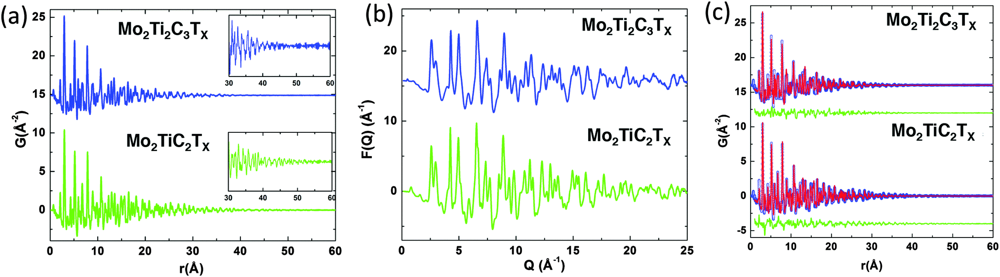 | ||
| Fig. 1 PDF analysis. (a) PDFs of two delaminated Mo–Ti MXene samples in the r-range up to 60 Å. Insets show expanded high-r region – from 30 Å to 60 Å – of both PDFs. (b) Reduced structure factor F(Q) of d-Mo2TiC2Tx (bottom) and d-Mo2Ti2C3Tx (top). (c) PDF fits of d-Mo2TiC2Tx and d-Mo2Ti2C3Tx. The blue circles, red solid lines correspond to measured and calculated results, respectively. The difference curves offset below are in green. | ||
To extract quantitative structural information, we carried out model fits to the PDF on both samples. In the modeling we create a single slab of atoms from a bulk lattice. For simplicity we perform a cylindrical cut where the diameter of the cylinder is allowed to vary. The PDF fit range was chosen to be 1 Å to 60 Å such that we would be able to obtain a complete structure of both materials. The PDFs of the best-fit models are compared to the data in Fig. 1c.
The ball and stick representations for the best-fit models for the d-Mo2TiC2Tx and d-Mo2Ti2C3Tx structures are displayed in Fig. 2a and b, respectively, and the refined structural parameters are summarized in Table 2. Since we built our single slab models by cutting from bulk crystalline lattices, in Table 2 we also report a and c lattice parameters, as well as fractional coordinates z, which are needed to define the bulk lattices. All parameters – except the c lattice parameters, c-LPs – were calculated from PDF analysis. The c-LPs were calculated from XRD patterns of the same samples (Fig. S1 in ESI†). The XRD patterns of both d-Mo2TiC2Tx and d-Mo2Ti2C3Tx show that all diffraction peaks disappeared, except (000l) peaks, which proves that when the delaminated flakes are restacked during vacuum filtration, they do so randomly and only keep the crystallographic ordering along the [000l] direction, forming a turbostratic structure. These results are in agreement with our previously reported XRD results.17 Based on the parameters presented in Table 2, undistorted structures of Mo2TiC2Tx and Mo2Ti2C3Tx are plotted in Fig. S2 (ESI†).
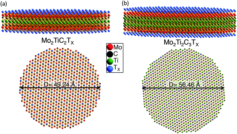 | ||
| Fig. 2 Polyhedral representation of Mo–Ti MXenes. (a) Mo2TiC2Tx and, (b) Mo2Ti2C3Tx structures. Each sample is shown in top and side views. Mo, Ti and C are depicted in red, green and black, respectively. Tx represents the surface terminations (O, F and OH) depicted in blue. | ||
| Mo2TiC2Tx | Mo2Ti2C3Tx | |
|---|---|---|
| R w | 0.196 | 0.206 |
| a (Å) | 2.9357 | 2.9598 |
| c (Å) | 36.1 | 45.5 |
| z (Mo) | 0.5719 | 0.5843 |
| z (Ti) | — | 0.5272 |
| z (C) | 0.5414 | 0.5564 |
| z (O/F) | 0.3918 | 0.3736 |
| U iso (Mo) (Å2) | 0.0036 | 0.0028 |
| U iso (Ti) (Å2) | 0.0025 | 0.0016 |
| U iso (C) (Å2) | 0.0039 | 0.0025 |
| U iso (O) (Å2) | 0.0032 | 0.0045 |
| U iso (F) (Å2) | 0.0038 | 0.0023 |
| Diameter (Å) | 49.24 | 56.46 |
| r (Mo–C) (Å) | 2.021 × 3 | 2.129 × 3 |
| r (Ti–C) (Å) | 2.260 × 6 | 2.110 × 3 |
| — | 2.165 × 3 | |
| r (Mo–O/F) (Å) | 2.142 × 3 | 1.916 × 1 |
Table 2 confirms that the atomic arrangement in Mo2TiC2Tx (Fig. S2 in ESI†) is quite similar to that previously reported for Ti3C2Tx.49 The main difference being that the Ti(1) atoms (two perimeter Ti layers) in Ti3C2 are replaced by Mo to form Mo2TiC2Tx. In the previously reported Ti3C2Tx structure, at 2.143 Å and 2.123 Å, both Ti(1)–C and Ti(2)–C bonds lengths, respectively, were similar.49 However, in Mo2TiC2Tx, at 2.021 Å, the Mo–C bonds are shorter than the Ti–C bonds at 2.260 Å. Not surprisingly, in the case of Mo2Ti2C3Tx the atomic arrangement (Fig. S2 in ESI†) is quite similar to the previously reported M4C3Tx MXene, viz. Nb4C3Tx.21 In the latter, for the Nb atom in the outer layers, the Nb–C bonds lengths were at 2.2217 Å and 2.1302 Å. At 2.2752 Å, the Nb–C bond lengths of the central carbons were very slightly longer. In Mo2Ti2C3Tx, all the Mo–C and Ti–C bonds have almost similar lengths (Table 2) and are slightly shorter than the Nb–C bonds in Nb4C3Tx.21
Experimental measurements of the electronic properties
DC transport measurements were performed to elucidate the effect of Mo introduction on the electronic properties. Fig. 3a shows the resistivity as a function of temperature measured on Ti3C2Tx and the Mo-containing MXenes. The resistivities of the d-Mo2TiC2Tx and d-Mo2Ti2C3Tx samples are lower than those of the multilayer samples, but the delaminated Mo-containing MXenes are almost one order of magnitude more resistive than the multilayer Ti3C2Tx.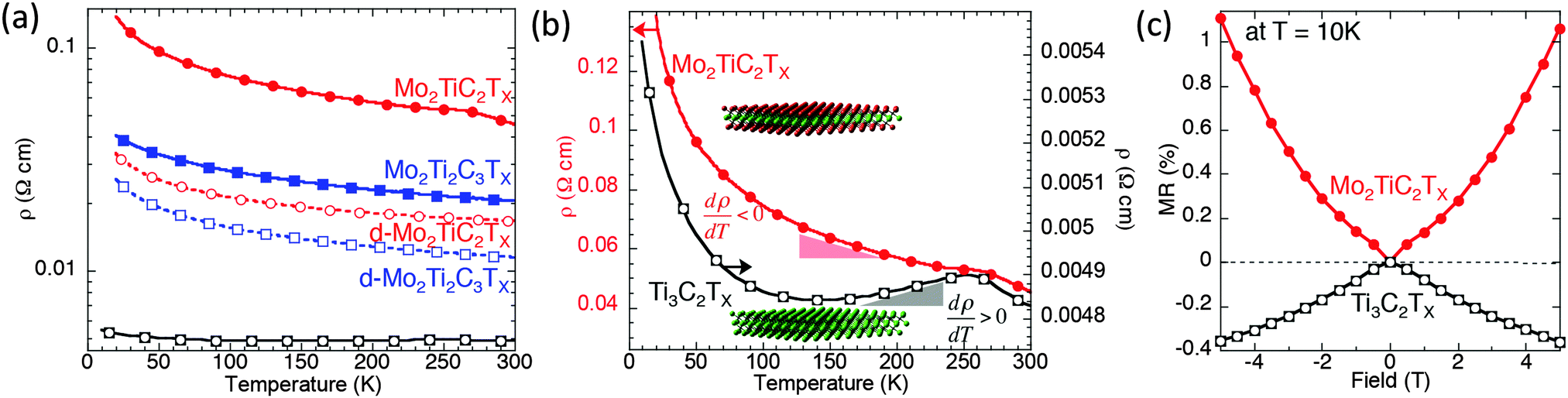 | ||
| Fig. 3 Transport properties. (a) Temperature dependence of resistivity for a Mo2TiC2Tx (red), Mo2Ti2C3Tx (blue), and Ti3C2Tx (black). The dashed lines represent delaminated films and the solid lines those of pressed multilayered powders. (b) Comparison of Mo2TiC2Tx (red, left side y-axis) and Ti3C2Tx (black, right-side y-axis) resistivity results. The colored triangles (red and black) below each resistivity curve illustrate the differences in dρ/dT. (c) Corresponding magnetic field dependent magnetoresistance taken at 10 K. | ||
In order to better reveal the difference between the Mo-containing MXenes and Ti3C2Tx, the resistivity values of a multilayered Mo2TiC2Tx (red, left-hand y-axis) and a multilayered Ti3C2Tx (black, right-side y-axis) are plotted in Fig. 3b. The overall resistivity between the two samples differs by roughly one order of magnitude and both samples exhibit a change in the behavior near 250 K, which is probably related to water and ions present between the MXene layers and will be discussed elsewhere. Notably, the behavior of Ti3C2Tx from 130–250 K is metallic (dρ/dT > 0), in contrast to Mo2TiC2Tx, in which the resistivity increases with decreasing temperature (dρ/dT < 0) over the measured range of 10–250 K. At temperatures below ∼130 K, the resistivity of Ti3C2 increases with decreasing temperature.
The Mo2TiC2Tx results shown in Fig. 3b cannot be well fit by an Arrhenius model describing simple semiconductor behavior or to any variable range hopping model, as shown in Fig. S3 in ESI.† Said otherwise, there could be other explanations, such as interflake hopping processes for example, for the modest increases in resistivities with decreasing temperatures apparent in Fig. 3. Clearly more work is needed before more definite conclusions can be drawn. This comment notwithstanding, it is clear that when Mo layers sandwich their Ti counterparts (in the Mo-based MXenes) the resistance increases monotonically with decreasing temperature, whereas in the absence of Mo, the resistance, at least initially decreases with decreasing temperature (Fig. 3b).
Since both MXenes have increasing resistivity at temperatures below 130 K, we measured their MR at 10 K to check if the mechanisms of the processes governing this behavior are the same. The MRs measured in the two materials are opposite in sign (Fig. 3c), suggesting fundamentally different transport mechanisms in Ti3C2Tx and Mo2TiC2Tx. The MR data, taken at 10 K in the regime where both samples exhibit dρ/dT < 0, are shown in Fig. 3c. We define MR (%) = (RH − R0) × 100/R0, where RH and R0 are the 5 T and zero-field resistivity, respectively. In agreement with Fig. 3c, a negative MR was previously reported for Ti3C2Tx within its dρ/dT < 0 regime and was attributed to weak localization.22 However, the presence of positive MR and a negative dρ/dT at all temperatures for Mo2TiC2Tx suggests a different transport mechanism is dominant in this Mo containing MXene than in Ti3C2Tx. To better understand and explain this behavior, we carried out an in-depth DFT study.
DFT results
In our previous work, non-spin-polarized simulations suggested the new bimetallic MXenes, in general, and the Mo–Ti ones in particular should be metallic.17 As shown here, macroscopic transport measurements suggest otherwise. This discrepancy may result from considering the wrong magnetic ground state, as some MXenes have been predicted to be magnetic.50,51 To shed more light on the problem, spin-polarized DFT calculations were performed on the Mo-MXenes with various magnetic orderings (presented in Table S1 and Fig. S4 in ESI†) as a function of 7 terminations for each compound. The terminations varied from –OH, –O, –F and combinations thereof (see Table S2, ESI†).The calculated total energies of non-magnetic and magnetic ordered states of Mo-based MXenes are shown in Table S2 (ESI†). In Table S2 (ESI†) the lowest total energy configuration is shown in bold. Based on these results it is obvious that in all cases, and for all terminations, the antiferromagnetic (AFM) ground states (total and in-plane) are the lowest in energy. The energy difference between some of the different AFM states, however, is quite small <10 meV. The differences between the AFM states and FM states are for the most part significantly higher.
The predicted a lattice parameters, a-LPs, and Mo–C, Ti–C, and Mo–O/F bond lengths of non-magnetic and theoretically most stable magnetic states are presented and compared with experimental results in Table S3 (ESI†). Two important and related observations are noteworthy. The first is that the predicted lattice parameters are ∼5–8% larger than the experimental ones. This overestimation most likely results from the GGA and Hubbard U approximations. The second observation is that in all cases the non-magnetic (NM) lattice parameters are closer to the experimental results than the AFM case. The reason for this state of affairs is not clear at this time. Along the same lines, the experimentally determined distance between the Mo and the O/F terminations, r(Mo–O/F), listed in Table 1, shows a noticeable reduction (∼0.2 Å) when going from Mo2TiC2Tx to Mo2Ti2C3Tx, which corresponds to larger theoretical lattice parameters.
To gain more insight into the magnetic properties, the spatial spin electron density distributions for Mo2TiC2(OH)2 and Mo2Ti2C2(OH)2 are computed and compared in Fig. 4. In this plot yellow represents spin up and blue, spin down. Clearly, the unpaired spin concentrates on the Mo atoms, implying the magnetism of Mo-MXene originates from unpaired Mo-3d orbitals. For single terminations, the spin-up and spin-down density is distributed equally. Although the mixed terminations also show overall AFM (see Fig. S5 in ESI†), the individual density of spin-up and spin-down is different. This should relate to the mixed Mo–O/F bonds. The corresponding total densities of states (DOS) of Mo-MXenes are shown in Fig. 5 (the projected DOS are shown in Fig. S6 in ESI†). Based on our calculations, –OH and –F terminated Mo-MXenes should be semiconductors, while OH-terminated MXenes have smaller band-gap ∼0.05 eV. In contrast, the O-terminated Mo-MXenes should show metallic behavior. Since from EDX analysis, it is apparent that the surfaces are terminated by both F and O/OH, we also examined the magnetic ordering and electronic structure of Mo-MXenes with mixed terminations (Fig. 5). The latter show semiconducting behavior, except for Mo2TiC2Tx at high –O concentrations. This suggests that the synthesized Mo-MXenes could be intrinsic semiconductors.
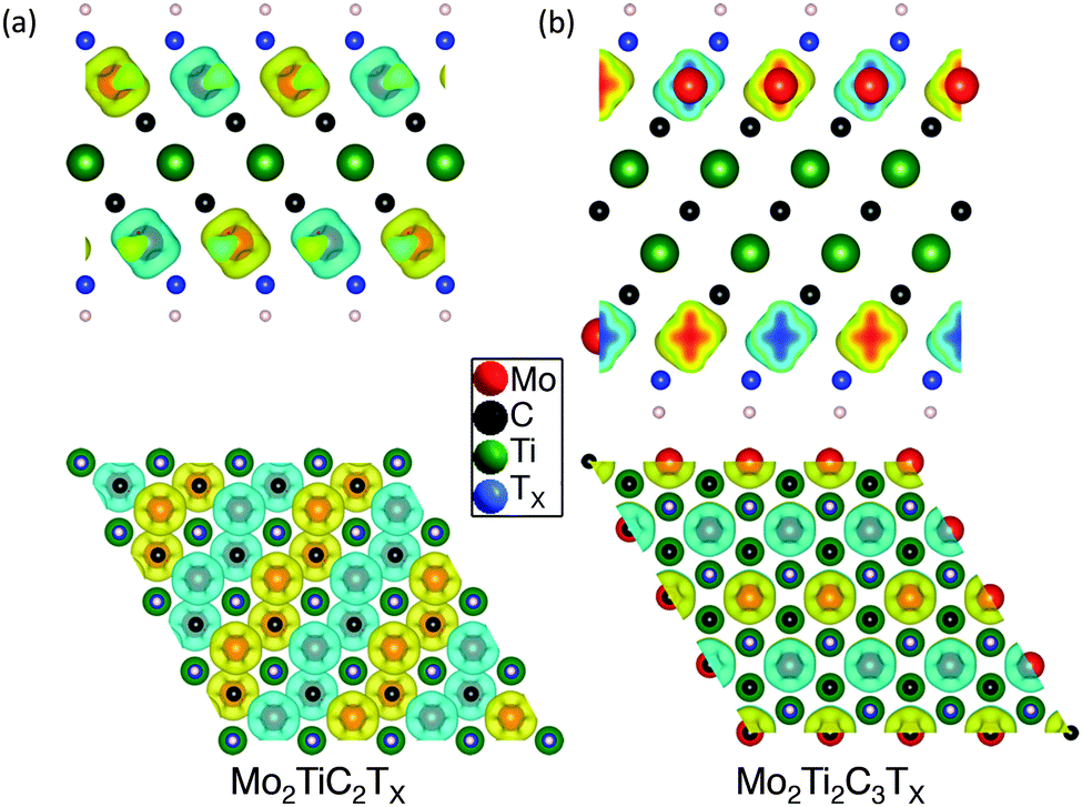 | ||
| Fig. 4 Spin density of Mo-MXenes. Top and side views of calculated spatial spin density distributions (up-down) of, (a) Mo2TiC2(OH)2 and, (b) Mo2Ti2C2(OH)2 compositions. Yellow – spin up; blue – spin down. | ||
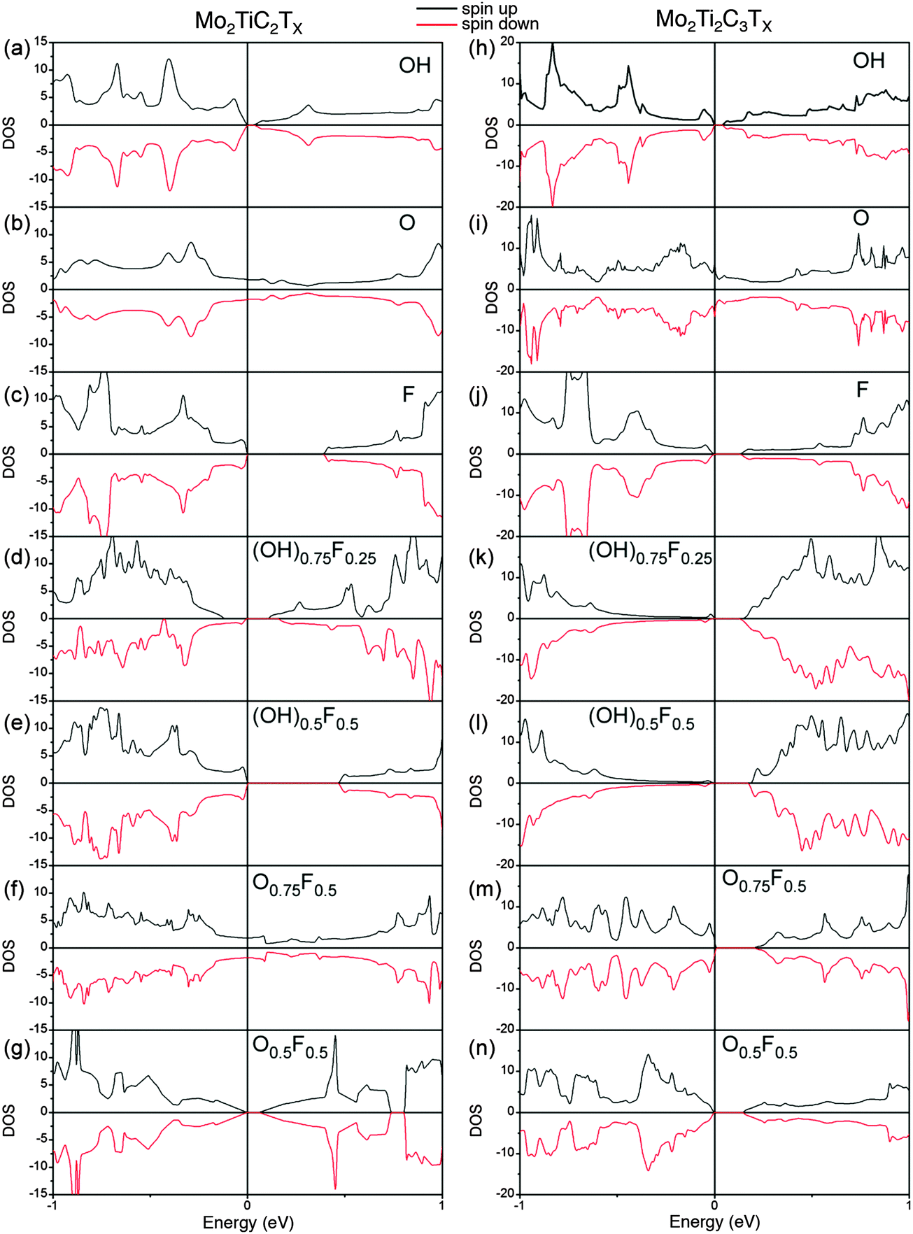 | ||
| Fig. 5 DFT analysis of electronic properties of MXenes with different terminations. Calculated total density of states (DOS) of (a)–(g) Mo2TiC2Tx and, (h)–(n) Mo2Ti2C3Tx as a function of terminations shown on the different panels. | ||
Conclusions
In summary, we report the full 3D structures of two new double transition metal MXenes, Mo2TiC2Tx and Mo2Ti2C3Tx, in which Mo atomic layers sandwich the Ti–C inner layers. Conductivity measurements and DFT calculations show that new chemical and structural degrees of freedom opening up in the 2D transition metal carbides may be used to control their electronic properties. While Ti3C2Tx is metallic and its resistivity decreases with temperature from 250 to 130 K, the resistivity of both Mo2TiC2Tx and Mo2Ti2C3Tx MXenes increase with decreasing temperature in the 250 to 10 K temperature range. The Ti3C2Tx resistivity also increases below 130 K, but never reaches the resistivity values of the Mo–Ti MXenes.Magnetoresistance measurements on Ti3C2Tx and its Mo-containing counterpart, Mo2TiC2Tx, at 10 K showed that they have opposite signs, suggesting fundamentally different transport mechanisms. We corroborated these measurements and analyses by DFT calculations and showed that replacing the two outer layers of Ti in Ti3C2(OH)2 by Mo, to form Mo2TiC2(OH)2, while keeping the same surface termination groups, changed the electronic structure to a semiconductor with a narrow band gap (∼0.05 eV). The same behavior is predicted for Mo2Ti2C3(OH)2.
In contrast to the previously reported methods for controlling the electronic properties, such as doping, phase change or changing surface termination, here we show that the electronic properties of 2D metal carbides can be tuned by replacing the outer metal layers with another metal. The combined experimental and theoretical results suggest semiconductor-like behavior of layered Mo–Ti MXenes. This opens a door to atomic-scale design of 2D materials for a variety of sensing, optical, electronic, electrochemical and other applications.
Acknowledgements
All authors are grateful to Dr Eric Dooryhee, Brookhaven National Laboratory, for experimental help and to NSLS-II for granting beam time at the XPD beamline. Use of the National Synchrotron Light Source II, Brookhaven National Laboratory, was supported by the US Department of Energy, Office of Science, Office of Basic Energy Sciences, under Contract No. DE-SC0012704. BA was supported by King Abdullah University of Science and Technology (KAUST)-Drexel University Competitive Research Grant (CRG 3). Work in the Billinge group was supported by US National Science Foundation through grant DMR-1534910. EJM and SJM were supported by the Army Research Office under grant number W911NF-15-1-0133. DFT (YX, PRCK) were supported as part of the Fluid Interface Reactions, Structures and Transport (FIRST) Center, an Energy Frontier Research Center funded by the U.S. Department of Energy, Office of Science, Office of Basic Energy Sciences. This research used resources of the National Energy Research Scientific Computing Center, a DOE Office of Science User Facility supported by the Office of Science of the U.S. Department of Energy under Contract No. DE-AC02-05CH11231.References
- V. Nicolosi, M. Chhowalla, M. G. Kanatzidis, M. S. Strano and J. N. Coleman, Science, 2013, 340, 1226419 CrossRef.
- G. Fiori, F. Bonaccorso, G. Iannaccone, T. Palacios, D. Neumaier, A. Seabaugh, S. K. Banerjee and L. Colombo, Nat. Nanotechnol., 2014, 9, 768–779 CrossRef CAS PubMed.
- F. Xia, H. Wang, D. Xiao, M. Dubey and A. Ramasubramaniam, Nat. Photonics, 2014, 8, 899–907 CrossRef CAS.
- F. Koppens, T. Mueller, P. Avouris, A. Ferrari, M. Vitiello and M. Polini, Nat. Nanotechnol., 2014, 9, 780–793 CrossRef CAS PubMed.
- D. Akinwande, N. Petrone and J. Hone, Nat. Commun., 2014, 5, 5678 CrossRef CAS PubMed.
- A. Cepellotti, G. Fugallo, L. Paulatto, M. Lazzeri, F. Mauri and N. Marzari, Nat. Commun., 2015, 6, 6400 CrossRef CAS PubMed.
- A. Geim and I. Grigorieva, Nature, 2013, 499, 419–425 CrossRef CAS PubMed.
- B. Lalmi, H. Oughaddou, H. Enriquez, A. Kara, S. Vizzini, B. Ealet and B. Aufray, Appl. Phys. Lett., 2010, 97, 223109 CrossRef.
- S. Cahangirov, M. Topsakal, E. Aktürk, H. Şahin and S. Ciraci, Phys. Rev. Lett., 2009, 102, 236804 CrossRef CAS PubMed.
- M. Dávila, L. Xian, S. Cahangirov, A. Rubio and G. Le Lay, New J. Phys., 2014, 16, 095002 CrossRef.
- H. Liu, A. T. Neal, Z. Zhu, Z. Luo, X. Xu, D. Tománek and P. D. Ye, ACS Nano, 2014, 8, 4033–4041 CrossRef CAS PubMed.
- L. Li, Y. Yu, G. J. Ye, Q. Ge, X. Ou, H. Wu, D. Feng, X. H. Chen and Y. Zhang, Nat. Nanotechnol., 2014, 9, 372–377 CrossRef CAS PubMed.
- C. Ataca, H. Sahin and S. Ciraci, J. Phys. Chem. C, 2012, 116, 8983–8999 CAS.
- M. Osada and T. Sasaki, Adv. Mater., 2012, 24, 210–228 CrossRef CAS PubMed.
- M. Naguib, M. Kurtoglu, V. Presser, J. Lu, J. Niu, M. Heon, L. Hultman, Y. Gogotsi and M. W. Barsoum, Adv. Mater., 2011, 23, 4248–4253 CrossRef CAS PubMed.
- M. Naguib, V. N. Mochalin, M. W. Barsoum and Y. Gogotsi, Adv. Mater., 2014, 26, 992–1004 CrossRef CAS PubMed.
- B. Anasori, Y. Xie, M. Beidaghi, J. Lu, B. C. Hosler, L. Hultman, P. R. C. Kent, Y. Gogotsi and M. W. Barsoum, ACS Nano, 2015, 9, 9507–9516 CrossRef CAS PubMed.
- M. Kurtoglu, M. Naguib, Y. Gogotsi and M. W. Barsoum, MRS Commun., 2012, 2, 133–137 CrossRef CAS.
- M. Khazaei, M. Arai, T. Sasaki, M. Estili and Y. Sakka, Phys. Chem. Chem. Phys., 2014, 16, 7841–7849 RSC.
- M. Khazaei, M. Arai, T. Sasaki, C.-Y. Chung, N. S. Venkataramanan, M. Estili, Y. Sakka and Y. Kawazoe, Adv. Funct. Mater., 2013, 23, 2185–2192 CrossRef CAS.
- M. Ghidiu, et al. , Chem. Commun., 2014, A31, 373–378 Search PubMed.
- J. Halim, et al. , Chem. Mater., 2014, 26, 2374–2381 CrossRef CAS PubMed.
- A. Miranda, J. Halim, M. Barsoum and A. Lorke, Appl. Phys. Lett., 2016, 108, 033102 CrossRef.
- S. Lai, J. Jeon, S. K. Jang, J. Xu, Y. J. Choi, J.-H. Park, E. Hwang and S. Lee, Nanoscale, 2015, 7, 19390–19396 RSC.
- J. Halim, et al. , Adv. Funct. Mater., 2016 DOI:10.1002/adfm.201505328.
- B. Anasori, et al. , J. Appl. Phys., 2015, 118, 094304 CrossRef.
- B. Anasori, J. Halim, J. Lu, C. A. Voigt, L. Hultman and M. W. Barsoum, Scr. Mater., 2015, 101, 5–7 CrossRef CAS.
- M. Naguib, R. R. Unocic, B. L. Armstrong and J. Nanda, Dalton Trans., 2015, 44, 9353–9358 RSC.
- P. J. Chupas, X. Qiu, J. C. Hanson, P. L. Lee, C. P. Grey and S. J. Billinge, J. Appl. Crystallogr., 2003, 36, 1342–1347 CrossRef CAS.
- X. Yang, P. Juhas, C. L. Farrow and S. J. Billinge, arXiv preprint arXiv:1402.3163, 2014.
- P. Juhás, T. Davis, C. L. Farrow and S. J. Billinge, J. Appl. Crystallogr., 2013, 46, 560–566 CrossRef.
- T. Egami and S. J. Billinge, Underneath the Bragg peaks: structural analysis of complex materials, Newnes, 2012, vol. 16 Search PubMed.
- T. Proffen and S. Billinge, J. Appl. Crystallogr., 1999, 32, 572–575 CrossRef CAS.
- C. Farrow, P. Juhas, J. Liu, D. Bryndin, E. Božin, J. Bloch, T. Proffen and S. Billinge, J. Phys.: Condens. Matter, 2007, 19, 335219 CrossRef CAS PubMed.
- P. Debye, Ann. Phys., 1915, 351, 809–823 CrossRef.
- P. Juhás, C. Farrow, X. Yang, K. Knox and S. Billinge, Acta Crystallogr., Sect. A: Found. Adv., 2015, 71, 562–568 Search PubMed.
- C. L. Farrow, D. K. Bediako, Y. Surendranath, D. G. Nocera and S. J. Billinge, J. Am. Chem. Soc., 2013, 135, 6403–6406 CrossRef CAS PubMed.
- A. N. Beecher, X. Yang, J. H. Palmer, A. L. LaGrassa, P. Juhas, S. J. Billinge and J. S. Owen, J. Am. Chem. Soc., 2014, 136, 10645–10653 CrossRef CAS PubMed.
- G. Cernuto, N. Masciocchi, A. Cervellino, G. M. Colonna and A. Guagliardi, J. Am. Chem. Soc., 2011, 133, 3114–3119 CrossRef CAS PubMed.
- W. Kohn and L. J. Sham, Phys. Rev., 1965, 140, A1133 CrossRef.
- P. E. Blöchl, Phys. Rev. B: Condens. Matter Mater. Phys., 1994, 50, 17953 CrossRef.
- G. Kresse and J. Furthmüller, Phys. Rev. B: Condens. Matter Mater. Phys., 1996, 54, 11169 CrossRef CAS.
- J. P. Perdew, K. Burke and M. Ernzerhof, Phys. Rev. Lett., 1996, 77, 3865 CrossRef CAS PubMed.
- M. Nolan, S. D. Elliott, J. S. Mulley, R. A. Bennett, M. Basham and P. Mulheran, Phys. Rev. B: Condens. Matter Mater. Phys., 2008, 77, 235424 CrossRef.
- G. Hautier, S. P. Ong, A. Jain, C. J. Moore and G. Ceder, Phys. Rev. B: Condens. Matter Mater. Phys., 2012, 85, 155208 CrossRef.
- H. J. Monkhorst and J. D. Pack, Phys. Rev. B: Solid State, 1976, 13, 5188 CrossRef.
- Y. Dall'Agnese, M. R. Lukatskaya, K. M. Cook, P.-L. Taberna, Y. Gogotsi and P. Simon, Electrochem. Commun., 2014, 48, 118–122 CrossRef.
- V. N. Borysiuk, V. N. Mochalin and Y. Gogotsi, Nanotechnology, 2015, 26, 265705 CrossRef PubMed.
- C. Shi, M. Beidaghi, M. Naguib, O. Mashtalir, Y. Gogotsi and S. J. Billinge, Phys. Rev. Lett., 2014, 112, 125501 CrossRef PubMed.
- J. Hu, B. Xu, C. Ouyang, S. A. Yang and Y. Yao, J. Phys. Chem. C, 2014, 118, 24274–24281 CAS.
- C. Si, J. Zhou and Z. Sun, ACS Appl. Mater. Interfaces, 2015, 7, 17510–17515 CAS.
Footnote |
| † Electronic supplementary information (ESI) available. See DOI: 10.1039/c5nh00125k |
| This journal is © The Royal Society of Chemistry 2016 |