
Hierarchical nanostructures of metal oxides for enhancing charge separation and transport in photoelectrochemical solar energy conversion systems
Haining
Chen
and
Shihe
Yang
*
Department of Chemistry, William Mong Institute of Nano Science and Technology, The Hong Kong University of Science and Technology, Clear Water Bay, Kowloon, Hong Kong, China. E-mail: chsyang@ust.hk
First published on 19th October 2015
Abstract
Photoelectrochemical solar energy conversion systems, including photoelectrochemical water splitting and photoelectrochemical solar cells (dye-sensitized solar cells, DSSCs), are under intensive development aiming at efficiently harvesting and utilizing solar energy. Metal oxides carved into hierarchical nanostructures are thought to be promising for improving photoelectrochemical performance by enhancing charge separation and transport. Herein, we review the recent progress in the research on the design and applications of metal oxide hierarchical nanostructures in water splitting and DSSC systems with a view to understanding how they improve the device performance in terms of enhanced charge separation and transport properties. This review will end with a conclusion on metal oxide hierarchical nanostructures together with potential future research directions thereof.
1. Introduction
As a clean and inexhaustible energy source, solar energy is the most important alternative to non-renewable fossil fuels to solve the problems of energy shortage, global warming and environmental pollution. The key issue is how to efficiently harvest and utilize solar energy. Photoelectrochemical (PEC) solar energy conversion is regarded as one of the most promising technologies for solar energy conversion and application.1–7 There are mainly two embodiments of PEC solar energy conversion, as defined in ref. 7: PEC water splitting and PEC solar cells. A PEC water splitting system aims to convert solar energy into chemical energy in terms of fuels such as H2.7–10 On the other hand, PEC solar cell systems, such as dye-sensitized solar cells (DSSCs) and quantum dot-sensitized solar cells (QDSCs),7,11,12 directly convert solar energy to electric energy. Thus far, much progress has been made from both fronts on PEC water splitting and PEC solar cells, primarily driven by the rapid advance of nanomaterials and nanotechnologies.What the PEC water splitting and PEC solar cell systems have in common are the main device structure and the working principle.6,7 In particular, photoelectrodes are at the core of these devices, which absorb light to generate electrons and holes, and sequentially separate and transport these charges.8,12 Metal oxide semiconductors (such as TiO2, ZnO, SnO2, Fe2O3, WO3, and BiVO4) are widely explored and used for photoelectrodes, or more precisely photoanodes, because of their suitable semiconducting properties, high stability, material abundance and facile nanostructuring.13,14 The charge separation and transport processes occurring at the photoelectrode/electrolyte interface and within the photoelectrode, respectively, are critical to device performance, which in turn greatly depends on the structure and morphology of the metal oxide semiconductor.7,8,12,15 In principle, a large contact area between the photoelectrode and the electrolyte is necessary to increase the areal density of separated electron–hole pairs generated from photoabsorption. Following this line of thinking, nanoparticle building blocks with a high surface-to-volume ratio are used to construct the photoelectrode.11,15 However, the catch is that small nanoparticle size is associated with numerous surface states and grain boundaries, which would hinder electron transport within the photoelectrode.15–17
Confronted by the conflicting issues of the nanoparticle photoelectrode, researchers have resorted to integral nanostructure design that can ensure both a high surface area and good charge transfer/transport. In this context, well-aligned nanoarrays have been exploited as a general photoelectrode structure, including nanowires,18–21 nanorods,22–27 nanotubes28–32 and nanosheet33–38 arrays, which efficiently shorten the electron transport path for charge collection. The improved electron transport is due to the single-crystalline nanounits in the nanoarrays and the elimination of grain boundaries.12,15,25 It should be pointed out that such nanoarray photoelectrodes are still limited by their relatively low surface area for charge separation and/or sensitizer deposition, arising from the difficulty in controlling the packing density and the size parameters of the nanounits.1,15 In the last few years, researchers have started to focus on constructing hierarchical nanostructures in the interest of a large surface area for maximizing charge separation without compromising the electron transport rate. These hierarchical nanostructures are commonly composed of trunks (highway transport) with a high charge transport rate and branches with a high surface-to-volume ratio (local transport).15,39–41
This review article attempts to document the important research progress in the last few years on hierarchical nanostructures of metal oxides for PEC solar energy conversion systems. Because of the breadth of the area, we are obliged to be selective by focusing on unique hierarchical nanostructural designs for enhancing charge separation and transport. Therefore, many important studies on metal oxide hierarchical nanostructures may be unfortunately omitted here, for which we refer the readers to other relevant review articles.1,39,41–49 In addition, since QDSCs themselves have formed a new branch with a similar working principle to DSSCs as well as similar nanostructures, they are not included in this review, and interested readers are referred to some recent reviews in this area.49–52
In the following, we will start by briefly introducing the working principles of hierarchical nanostructure photoelectrodes in PEC solar energy conversion systems with emphasis on the charge separation and transport behaviors. Then the most recent research progress on metal oxide hierarchical nanostructures for PEC water splitting and DSSCs will be sequentially presented and discussed. Finally, we will draw a conclusion and present potential future research directions for higher performance metal oxide hierarchical nanostructure photoelectrodes.
2. PEC solar energy conversion with metal oxide hierarchical nanostructures
The general working principles for PEC solar energy conversion systems (water splitting and DSSCs) are rather similar. Fig. 1 illustrates the charge separation and transport processes together with the energy level diagrams for PEC water splitting and DSSC systems with an n-type oxide semiconductor. In the water splitting system (Fig. 1(A)), photons with an energy exceeding the band gap of oxides generate electron–hole pairs, which are separated by the electric field present in the space-charge layer.7 Electrons move across the oxide semiconductor to the current collector and reach the counter electrode through an external circuit to reduce water to H2, while holes are driven toward the surface to oxidize water to O2.8 Therefore, the electron transport in the oxide semiconductor and the hole transfer across the surface of the oxide semiconductor are two important processes in the water splitting photoelectrode. Clearly, rapid electron transport and efficient hole transfer will reduce charge recombination loss, which are consequently prerequisite for designing high performance water splitting devices. | ||
| Fig. 1 Schematic illustrating the charge separation and transport processes in photoelectrochemical solar energy conversion systems: (A) PEC water splitting and (B) DSSC systems. ECB, EVB and EF represent the bottom of the conduction band (CB), the top of the valence band (VB), and the Fermi level of the oxide semiconductor, respectively, while EO/R represents the energy level of the water oxidization or the regenerating species in the electrolyte. | ||
In the DSSC system, as shown in Fig. 1(B), dye molecules are used as sensitizers to harvest sunlight. In the photoelectrode, therefore, photons are mainly absorbed by the sensitizers to generate electron–hole pairs.11,12 The electrons are then injected into the conduction band (CB) of the oxide semiconductor and are transported toward the counter electrode through an external circuit to reduce the oxidized form of the redox relay molecules (I−/I3− redox couple11,12), while holes are scavenged at the surface by the reduced form of the redox relay molecules. In this kind of system, the processes of electron injection to and transport in the oxide semiconductor and the hole transfer to the electrolyte should all be efficient to avoid charge recombination losses and thereby obtain an overall high-performance. Fortunately, the charge separation (electron injection into the metal oxide and hole extraction by the electrolyte) in DSSCs is commonly efficient due to the monolayer of dyes separating the two parts and the judicious design of the dye molecules. Thus the remaining critical issue for device performance is electron transport in the metal oxide semiconductor. Faster electron transport would lead to a lower recombination between energetic electrons in the metal oxide and the electrolyte and thus a higher device performance.
In photoelectrochemical systems, a large specific surface area is usually necessary for the photoelectrodes to achieve high performance because it will provide ample sites for separating the photogenerated charges in water-splitting devices and for dye loading in DSSCs. Therefore, nanostructured photoelectrodes are usually adopted. Fig. 2 illustrates three typical oxide nanostructure photoelectrodes used in photoelectrochemical systems and their corresponding charge transfer and transport behaviors. The first photoelectrode consists of randomly assembled nanoparticles (NPs), in which a large surface area (a specific surface area of 780 cm2 per cm2 of geometric surface for the film fabricated by 15 nm NPs)7,41 could afford numerous charge separation sites at the photoelectrode/electrolyte interface for water-splitting devices and allows deposition of a large amount of sensitizers for DSSCs. However, charge transport in such NP electrodes is greatly limited due to the presence of numerous grain boundaries and high surface state density. For example, the electron diffusion coefficient (Dn) of a TiO2 NP film is about 5 × 10⁻⁵ cm2 s−1, which is several orders of magnitude lower than that of a single crystalline TiO2 (0.4 cm2 s−1), and hence limits its diffusion length (Ln) to about 7–30 μm.53–55
 | ||
| Fig. 2 Schematic illustrating three typical photoelectrodes and their corresponding charge separation/transport behaviors. | ||
The second photoelectrode is made of nanoarrays, in which well-aligned and/or single-crystalline nanostructures would favor the charge transport. Indeed, a diffusion length Ln up to 100 μm has been reported for such nanoarrays.56 However, the remaining challenge is the relatively low surface area of such nanoarrays, which is insufficient for efficiently separating the photogenerated charge carriers and for depositing a large amount of dyes. This challenge can be taken up by the third photoelectrode, which is characterized by hierarchical nanostructures such as branched-nanoarrays. In a hierarchical nanostructure, the trunk can act as a rapid charge transport pathway while the branches outreach to increase the interfacial charge separation and/or dye deposition. Therefore, in photoelectrochemical systems, hierarchical nanostructures are usually designed to increase the surface area of nanoarray photoelectrodes but without obviously compromising their charge transport rates. By careful design, such hierarchical nanostructures should be able to achieve higher performance than the NP and nanoarray counterparts. Up to now, nanoarrays have been extended to nanorods (NRs), nanowires (NWs), nanotubes (NTs), nanosheets (NSs) and nanotetrapod (NTP) arrays, while branched arrays have comprised nanounits of NPs, NRs, NWs, NTs and NSs.
3. Hierarchical nanostructures in water splitting systems
We focus on PEC water splitting systems using metal oxides as the photoelectrode for both light absorption and charge transfer/transport. As mentioned above, charge separation in a NP film is commonly efficient. However, charge transport in a NP film is obviously limited by the large number of grain boundaries. In fact, in addition to the low charge transport rate, another serious problem faced by NP films is their significantly lower light scattering capacity than nanoarray films and hence much lower light absorptivity, as shown in Fig. 3.57 As a result, NP films usually give a considerably lower water splitting performance than NR films. | ||
| Fig. 3 Light absorption plus scattering curves of the TiO2 NP, NR, and NR/NR in the wavelength range from 300 nm to 700 nm. Reproduced with permission from ref. 57. | ||
However, the small surface area of a nanoarray film due to its large unit size means limited sites for driving the charge separation processes, compromising the water splitting performance, especially when the water oxidation kinetics are sluggish. This becomes more serious for metal oxides with short hole diffusion lengths (Ln), such as α-Fe2O3 (Ln = 2–4 nm)58 and BiVO4 (Ln = 70–100 nm).59 Therefore, it is highly desirable to increase the surface area of the nanoarrays for efficient charge separation, and building branching nanoarrays with small nanounits is widely thought to be a promising strategy in that direction.
3.1 Branched-1D nanoarray photoelectrodes
1D nanoarrays are the most common kind of nanoarrays that provide a direct and rapid electron transport pathway toward the collection substrate, and over the past few years, branching 1D nanoarrays have been widely explored in water splitting systems. In 2011, Zheng et al. first applied branched-TiO2 NR (NR/NR) arrays for water splitting and systematically compared the performance of NP, NR, and NR/NR photoelectrodes, which are illustrated in Fig. 4(A).57 Both the NR trunk and NR branches were prepared by a seed-assisted hydrothermal method using FTO and FTO/NRs as substrates, respectively, which were both single-crystalline rutile TiO2. As indicated in Fig. 4(B), the needle-shaped NR branches of about 50 nm long and 10 nm wide were grown uniformly on the NR trunks whose diameter was about 100 nm. After branching, the roughness factor of NR/NRs was greatly increased from 32 to 130, though it was still lower than that of the NP film (210). TiO2 NRs and NR/NRs exhibited similar light absorption properties, obviously higher than TiO2 NPs, especially at λ < 420 nm, as shown in Fig. 3, due to enhanced light scattering between NRs. From the J–V curves shown in Fig. 4(C), the photocurrent densities of the NPs, NRs, and NR/NRs are 0.01, 0.31 and 0.83 mA cm−2 at 0.8 V (vs. RHE), respectively. The very low photocurrent density for NPs was thought to be due to the low light absorption and slow charge transport. The J–V curve of TiO2 NR/NRs exhibits a steeper increase in current as the potential scanning in the positive direction with a saturated photocurrent density at 0.6 V (vs. RHE), suggesting much more efficient charge separation and transport. | ||
| Fig. 4 TiO2 NR/NR nanostructure arrays as water splitting photoelectrodes. (A) Schematic description of TiO2 NP, NR, and NR/NR photoelectrodes. (B) TEM image of the TiO2 NR/NR nanostructure. (C) Chopped J–V curves under a xenon lamp (UV portion of the spectrum matched to AM 1.5G, 88 mW cm−2) illumination. Reproduced with permission from ref. 57. | ||
Besides branched-TiO2 NR arrays, branched-ZnO NR arrays (ZnO NR/NRs) were also fabricated and tested as water splitting photoelectrodes.60 Similarly, a two-step seed-assisted hydrothermal method was exploited for NR trunk and NR branch growth. The ZnO NR/NR photoelectrode exhibited more than twice the photocurrent density of the ZnO NR photoelectrode at 1.2 V (vs. Ag/AgCl) under one-sun illumination. The highest solar-to-hydrogen conversion efficiency (STH) value for the ZnO NR/NR photoelectrode was 0.299%, obviously higher than that of the ZnO NR photoelectrode (0.236%). Therefore, branched-1D nanoarrays have well proved to be promising photoelectrode structures for water splitting.
3.2 Branched-nanotetrapod hierarchical nanostructures
In addition to 1D nanoarrays, other nanostructures have also been exploited as trunks for oxide hierarchical nanostructures. Nanotetrapods (NTPs) are one of the promising trunk structures, which consist of four rod-shaped nanostructures joining at a central core with tetrahedral angles. Size-tunable ZnO NTPs were successfully synthesized in our laboratory in 200761 and recently, we explored them to construct various types of photoelectrodes.62–66 However, ZnO NTPs alone are still limited by their small surface area. In order to solve this problem, we further branched ZnO NTPs for water splitting systems.67Fig. 5(A) shows the structure and charge generation, transfer and transport processes of a branched tetrapod array electrode.1 NR branches increased the surface area for enhancing charge separation and NTPs served as the charge transport pathway. For the construction, a ZnO NTP film was first prepared by a doctor-blade method and a seed-assisted hydrothermal process was exploited to grow NR branches on the NTP trunks. However, the surface of the NTPs was really smooth, which made it hard to deposit ZnO seeds by simply coating a seed solution. Therefore, an etching method was used to in situ produce seeds on the NTP trunks.68Fig. 5(B) illustrates the typical final morphology of ZnO NTP/NR photoelectrodes. The J–V curves in Fig. 5(C) indicate that the ZnO NTP photoelectrode only had a photocurrent density of 0.046 mA cm2 at 0.31 V (vs. Ag/AgCl) under one-sun illumination, while the ZnO NTP/NR photoelectrode promoted the photocurrent density to 0.12 mA cm2 at 0.31 V (vs. Ag/AgCl). The increase in the surface area for NTP/NR photoelectrodes was the main reason for the improvement in photocurrent density, which could enhance the charge separation at the photoelectrode/electrolyte interface. After being doped with the N element, the photocurrent density was further increased up to 0.99 mA cm−2 at 0.31 V (vs. Ag/AgCl) due to enhanced light absorption and utilization in the visible region.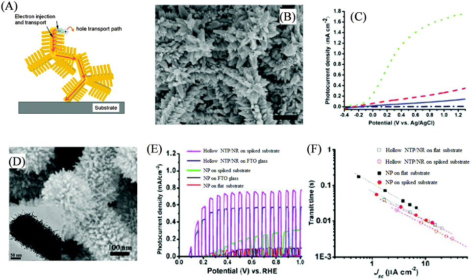 | ||
| Fig. 5 NTP-based hierarchical nanostructure as a water splitting photoelectrode. (A) Schematic illustrating charge generation, transfer and transport in NTP/NR. Reproduced with permission from ref. 1. (B) SEM image of the ZnO NTP/NR nanostructure. (C) J–V curves of the ZnO NTP in the dark (dot-dashed line), ZnO NTP (solid line), ZnO NTP/NR (dashed line), and N-doped ZnO NTP/NR (dotted line). Reproduced with permission from ref. 67. (D) SEM image of hollow TiO2 NTP/NR. Inset is the TEM image. (E) J–V curves and (F) transit time (transport time) of the water splitting photoelectrodes based on different nanostructures on different substrates. Reproduced with permission from ref. 69. | ||
Recently, we also synthesized and exploited hollow TiO2 NTP/NR hierarchical nanostructures as water splitting photoelectrodes. The synthesis was achieved by dissolution and nucleation processes on a ZnO NTP template.69 The reaction was conducted in an aqueous solution containing (NH4)2TiF6 and H3BO3 through the following steps:70,71
| TiF62− + H2O → TiO2 + 4H− + 6F− | (1) |
| BO33− + 6H+ + 4F− → 3H2O + BF4− | (2) |
| ZnO + 2H+ → Zn2+ + H2O | (3) |
3.3 Treelike hierarchical nanostructures
Hematite (α-Fe2O3) with a band gap of 2.1 eV has attracted broad interest as a water splitting photoelectrode material because of its low-cost, earth-abundance and high theoretical STH of 14–17%, corresponding to a photocurrent density of 11–14 mA cm−2 under one-sun illumination.72 However, its disadvantages are also obvious, such as a relatively low absorption coefficient, poor majority carrier conductivity and short diffusion length (LD = 2–4 nm) of minority carriers, meaning that enhancing light absorption by increasing film thickness would result in serious charge recombination losses.58 As such, a nanostructure design strategy is important to increase light absorption without increasing hole transfer distances and electron transport pathway lengths. In 2006, Grätzel and coworkers developed promising treelike α-Fe2O3 hierarchical nanostructures by the vapor phase deposition (VPD) method.73 This treelike nanostructure is highly porous with the topmost nanocrystals of about 20–40 nm in diameter for undoped α-Fe2O3 and 10–20 nm in diameter for Si-doped α-Fe2O3, which could afford efficient charge separation. Oriented attachment of these nanocrystals during growth was thought to lead to efficient charge transport. As a result, the Si-doped α-Fe2O3 treelike nanostructure achieved a photocurrent density of 2.2 mA cm−2 at 1.23 V (vs. RHE) under one-sun illumination. And it was revealed that the VPD parameters (e.g., air flow rate) greatly influenced the oriented attachment of α-Fe2O3 nanoparticles in the treelike nanostructure, thus impacting the PEC performance. By increasing the air flow rate from the previous 2 L min−1 (2L photoelectrode) to 6 L min−1 (6L photoelectrode), the gas residence time was shortened and the particle/precursor ratio was reduced, resulting in better adhesion between the particles while attached to the growing film. The better particle attachment has endowed the 6L photoelectrode with an obviously enhanced photocurrent density of over 3 mA cm−2 while using IrO2 as the catalyst.74Although the treelike nanostructure (especially the 6L photoelectrode) has achieved a promising performance, the structural characteristics of this hematite structure responsible for the performance were not clear at the time. For example, the reason as to why the 2L and 6L photoelectrodes with similar morphologies exhibited obviously different performances still needs more in-depth investigation. To clarify this issue, Warren et al. adapted a dark-field TEM (DF-TEM) in combination with conducting atomic force microscopy (C-AFM) to get information about the correlation between the spatial distribution of crystalline and current-carrying domains.75 The 2L and 6L photoelectrodes were chosen as the research subjects. Although the morphologies of the two samples were similar (Fig. 6(A) and (B)), the water-splitting performance was significantly different, as mentioned above. According to DF-TEM results (Fig. 6(C) and (D)), the nanocrystal aggregates in the 2L photoelectrodes had about 75% high-angle grain boundaries, significantly higher than those in the 6L photoelectrodes (18%). From the C-AFM results (current maps in Fig. 6(E) and (F)), high-angle grain boundaries mainly decreased the photocurrent by generating a potential barrier and hence blocking the transport of the majority carrier between adjacent crystals. Therefore this study suggests that it is important to reduce the high-angle grain boundaries in nanocrystal aggregates to get high photocurrent.
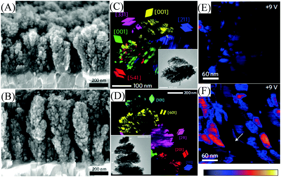 | ||
| Fig. 6 Fe2O3 nanotree as a water splitting photoelectrode. Cross-sectional SEM images of (A) 2L and (B) 6L photoelectrodes. Reproduced with permission from ref. 74. DF-TEM images of (C) 2L and (D) 6L photoelectrodes. Insets in (C) and (D) are the corresponding BF-TEM images. Each set of parallelograms defined the crystallographic orientation of the corresponding region of the DF-TEM. C-AFM current maps of (E) 2L and (F) 6L photoelectrodes at a tip-sample voltage of 9 V. The color scales represent a current variation from 0 (black) to 5 nA. Reproduced with permission from ref. 75. | ||
3.4 Single-crystalline hierarchical nanostructures
In the above, we have shown that branching 1D nanoarrays and NTPs were an effective approach to promote water splitting performance. However, grain boundaries were present between the trunks and branches, which still limited the charge transport rate. In our recent work, we exploited an epitaxial growth strategy to eliminate the grain boundary between the trunk and branches, which is actually also in the spirit of reducing the aforementioned high-angle grain boundaries. Specifically, a ZnO nanodisk (ND) was epitaxially grown on a ZnO NW to form a single-crystalline ZnO NW/ND nanostructure, as illustrated in Fig. 7(A). The ZnO ND was epitaxially grown on the NW by a modified hydrothermal process, in which sodium citrate was added into the reaction solution as an additive. As presented in Fig. 7(B), the ZnO NW was uniformly covered with a tiny ND that was vertical to the NW. The ND was about tens of nanometers thick, which obviously increased the roughness factor from 219 to 363. The spotted electron diffraction pattern (Fig. 7(C)) proved the single-crystalline structure of the ZnO NW/ND, which was further supported by the coincident lattice fringes (such as (0001) planes) between the NW and the ND in the HRTEM image (Fig. 7(D)). The formation of the ND resulted from the absorption of citrate anions on the (0001) planes to form complexes with Zn2+ ions, which greatly suppressed the growth rate along the [0001] direction. And as a result, the ND had large exposed (0001) and (000−1) facets. The electron diffusion coefficients (Dn) determined by the IMPS technique (Fig. 7(E)) indicated that at the same current density, the NW/ND had very close Dn to the NW, suggesting that the rapid charge transport properties of the NW were retained after single-crystalline branching. As a water splitting photoelectrode, the single-crystalline ZnO NW/ND had a significantly higher photocurrent density than the ZnO NW in the whole potential range (Fig. 7(F)). Enhanced light utilization and the larger surface area (about 66% enlargement) for charge separation in the single-crystalline ZnO NW/ND photoelectrode were the important causes. And the observation of a steeper increase in photocurrent density with respect to potential scanning and a saturated photocurrent density at 0.7 V (vs. Ag/AgCl) confirmed the much more efficient charge separation and collection in the ZnO NW/ND photoelectrodes. Besides, the polar facet of the ZnO ND was also proposed to favor the charge separation at the interface.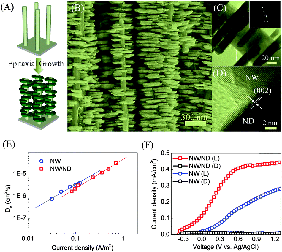 | ||
| Fig. 7 Single-crystalline ZnO NW/ND nanostructure as a water splitting photoelectrode. (A) Schematic illustrating the epitaxial growth of ZnO ND on NW. (B) SEM, (C) TEM and (D) HRTEM images of the single-crystalline ZnO NW/ND nanostructure. (E) Electron diffusion coefficient (Dn) as a function of current density. (F) J–V curves of ZnO NW/ND and ZnO NW obtained in the dark (D) and under one-sun illumination (L). Reproduced with permission from ref. 76. | ||
4. Hierarchical nanostructures in DSSC systems
In DSSCs, light absorption and electron transport are performed by a monolayer of dye molecules and the host metal oxides separately, and because of such a unique structure, the charge separation at the photoelectrode/electrolyte interface is typically rather efficient. Since a sufficient amount of dye molecules in the form of a monolayer is necessary to absorb most of the sunlight, the metal oxide electrode needs to have a large surface for dye loading and should be able to rapidly transport the injected electrons for collection, while avoiding recombination. The commonly used NP films could offer a large specific surface area but the film thickness was usually limited to about 10 μm due to their poor electron transport properties, resulting in low current densities which are about 55–75% of their theoretical maximum value for full sunlight illumination.12,21 The strategy for exploiting a long well-aligned nanoarray whose electron diffusion length is considerably longer than that of NPs was not very successful because the large size of nanounits and large gaps between them compromised the specific surface area.Hierarchical nanostructures were developed for DSSC systems aiming to utilize small size branches to increase the specific surface of the nanoarray trunks without obviously sacrificing their electron transport rate. Such hierarchical nanostructures include TiO2- and ZnO-based photoelectrodes, such as TiO2 NW/NR,77–80 TiO2 NT/NR,81 TiO2 NT/NP,82 TiO2 NT/NS,83 ZnO NW/NR,84–87 ZnO NS/NR,88,89 and ZnO NW/NS.90,91 However, the larger size trunks and/or branches than the NP counterparts did not provide a sufficient specific surface area for dye deposition. This can be appreciated from Fig. 8, which makes a surface area comparison between some different hierarchical nanostructures and NP films using data from the literature.21,80,81,84,88,90,92–95 As a result, earlier reported TiO2 or ZnO hierarchical nanostructures usually exhibited lower photocurrent density and PCE than their NP counterparts in DSSCs.96–98
 | ||
| Fig. 8 Surface area comparison among different hierarchical nanostructures and NP films based on the loading amount of N719 dye molecules.21,80,81,84,88,90,92–95 The dye loading using other dyes was converted to the N719 dye according to their relative molecule area. The corresponding film thicknesses are marked. The sizes of TiO2 and ZnO NPs are typically about 15–30 nm in diameter.21,93,95 | ||
In recent years, some promising hierarchical nanostructures have been reported with larger specific surface areas and/or strong light scattering features that can compensate surface area losses, such as multi-level hierarchical nanostructures and hierarchical spherical aggregate nanostructures. Besides, the application of hierarchical nanostructures in solid-state DSSCs is gaining interest because well-aligned nanoarrays are amenable to deep penetration of the electrolyte in comparison to NP films. In addition, single-crystalline hierarchical nanostructures were also successfully synthesized as promising photoelectrode candidates for DSSCs.
4.1 Multi-level hierarchical nanostructures
During the last few years, Kuang and coworkers established a systematic strategy to grow TiO2 multi-level hierarchical nanostructures based on anatase TiO2 NWs. Fig. 9(A) illustrates the evolution of typical TiO2 NW/NR/NR hierarchical nanostructures.99 Long anatase TiO2 NW arrays with a smooth surface were grown by their self-developed hydrothermal method using a reaction solution of potassium titanium oxide oxalate dehydrate (PTO)/H2O/diethylene glycol (DEG). And TiO2 NW/NR and TiO2 NW/NR/NR nanostructures were synthesized by immersing TiO2 NW and TiO2 NW/NR nanostructures in the above PTO/H2O/DEG reaction solution, respectively. The trunk of the final TiO2 NW/NR/NR photoelectrode was about 8 μm in length with a diameter of about 200–400 nm (Fig. 9(B)), while the NR branches formed at the second step were about 300–500 nm in length and about 10–20 nm in diameter. In the third step, numerous tiny NRs with an average size of 3–5 nm were randomly grown on the aforementioned nanorod branches. Dye absorption test experiments for different photoelectrodes with similar thickness of 8 μm indicated that dye uptakes have the following order of NW (3.76 × 10⁻⁸ mol cm−2) < NW/NR (6.35 × 10⁻⁸ mol cm−2) < NP (8.86 × 10⁻⁸ mol cm2) < NW/NR/NR (9.01 × 10⁻⁸ mol cm−2). The multi-level hierarchical nanostructure of TiO2 NW/NR/NR has obtained a larger surface area than the NP counterpart at a similar thickness. The charge transport and recombination property measurements indicated that TiO2 NW/NR/NR also had a lower transport time and longer electron lifetime than TiO2 NPs (Fig. 9(C) and (D)) due to the presence of the fast charge-transport TiO2 NW trunks. As a consequence, TiO2 NW/NR/NR had the highest PCE (8.11%) among the different photoelectrodes, obviously higher than that of NP photoelectrodes (6.32%), as presented in Fig. 9(E). | ||
| Fig. 9 TiO2 NW/NS/NR nanostructure as a DSSC photoelectrode. (A) Schematic illustrating the structures of TiO2 NW, NW/NR and NW/NR/NR. (B) SEM images of the TiO2 NW/NR/NR nanostructure. (C) Transport time, (D) electron lifetime and (E) J–V curves of the DSSCs based on different nanostructures. Reproduced with permission from ref. 93. | ||
Very recently, they exploited a relatively large size TiO2 NS (named as TiO2 NW/NS/NR) as first-level branches for enhancing light scattering to build a balance between the specific surface area and light trapping capacity. Though the final TiO2 NW/NS/NR nanostructure has a slightly smaller surface area than the NP film (1.51 × 10⁻⁷ mol cm−2vs. 1.58 × 10⁻⁷ mol cm−2), it still had a considerably higher Jsc (16.71 mA cm−2) and PCE (9.09%) in DSSCs than NP films (Jsc = 13.53 mA cm−2 and PCE = 7.55%).99 And soon afterwards, through layer-by-layer assembly of hyperbranched hierarchical tree-like TiO2 NWs (under layer), branched hierarchical rambutan-like TiO2 hollow submicrometer-sized spheres (intermediate layer) and hyperbranched hierarchical urchin-like TiO2 micrometer-sized spheres (top layer), their newly developed multi-layer hierarchical nanostructure photoelectrode successfully boosted the PCE of DSSCs up to 11.01%.100
4.2 Hierarchical spherical aggregate nanostructures
Hierarchical spherical aggregates have emerged as promising photoelectrode structures to enhance the light harvesting efficiency of nanoparticle-based photoanodes and to accelerate electron transport without sacrificing the specific surface area. A typical hierarchical spherical aggregate nanostructure (ZnO) is illustrated in Fig. 10(A), which was first explored as the photoelectrode in DSSCs by Cao et al. and was synthesized (Fig. 10(B)) by hydrolysis of zinc salt in a polyol medium at an elevated temperature (160 °C).48,101 The ZnO aggregate photoelectrode exhibited a considerably higher light scattering capacity than the ZnO nanoparticle photoelectrode, which as a result led to a greatly enhanced PCE (3.51%) than that with the nanoparticle photoelectrode (0.6%). The researchers pushed the PCE to 5.4%102 by employing polydisperse ZnO aggregates and further boosted the PCE to 6.3% by coating the ZnO aggregates with a thin TiO2 layer to suppress recombination.103 By employing the spray pyrolysis method to deposit the polydispersed ZnO aggregates in situ on a substrate, Sberveglieri et al. have successfully promoted the PCE of ZnO-based DSSCs to a record value of 7.5%.104 | ||
| Fig. 10 Hierarchical spherical aggregate nanostructures studied for DSSC photoelectrodes. (A) Scheme and (B) SEM image of ZnO aggregates. (C) UV-vis spectra of a ZnO aggregate film and a ZnO nanoparticle film. (D) J–V curves of the DSSCs based on a ZnO aggregate film and a ZnO nanoparticle film. Reproduced with permission from ref. 101. (E) Dnvs. charge density curves of the photoelectrodes based on a TiO2 aggregate film and a P25 TiO2 nanoparticle film. Reproduced with permission from ref. 108. (F) TEM image and scheme of oriented mesoporous TiO2 microspheres. Reproduced with permission from ref. 111. | ||
In parallel, TiO2 spherical aggregates have also been well documented with a structure similar to that of the aforementioned ZnO aggregates. For such materials, solvothermal treatment of amorphous precursor TiO2 spheres is a well established synthesis method.105–110 Dye loading measurements have demonstrated an obviously higher loading amount of about 8.69 × 10⁻⁵ mol g−1 for TiO2 aggregate powder than that for P25 TiO2 nanoparticles (4.25 × 10⁻⁵ mol g−1).105 Besides the high light scattering capacity and a larger surface area, TiO2 aggregates were confirmed to accelerate the electron transport in the photoelectrode (Fig. 10(E)),108 possibly due to the enhanced interconnection between different aggregates. So far, the TiO2 nanoparticle aggregates have garnered a high PCE of over 10%.108
Most recently, Zhao et al. have exploited a simple evaporation-driven oriented assembly method to synthesize a new kind of TiO2 spherical aggregate—three-dimensional open mesoporous TiO2 microspheres—as shown in Fig. 10(F).111 This kind of TiO2 microsphere exhibited well-controlled radially oriented hexagonal mesochannels and crystalline anatase walls, which greatly enhanced the surface area of the photoelectrode with an N719 dye uptake of 2.13 × 10⁻⁷ mol cm−2, about twice those of P25 TiO2 (1.12 × 10⁻⁷ mol cm−2) as well as the above mentioned TiO2 aggregates (1.45 × 10⁻⁷ mol cm−2). At the same time, this photoelectrode also exhibited an obviously longer electron lifetime and higher Dn, leading to a record certified PCE value of over 12%.
4.3 Hierarchical nanostructures in solid-state DSSCs
For high performance solid-state DSSCs (ssDSSCs), thorough penetration of a solid-state electrolyte into the mesoscopic photoelectrode is an important challenge. The difficulty has limited the NP film thickness to a few micrometers. On this point, hierarchical nanostructures have obvious advantages over NP films since well-aligned nanoarrays allow deep penetration into the solid-state electrolyte. And through careful optimization, hierarchical nanostructures are expected to permit a large amount of dye deposition together with good electrolyte penetration.Kim et al. have shown that pine tree-like TiO2 NT arrays (PTT), which were grown by a one-step hydrothermal method in a PTO/DEG/H2O solution,112 are promising hierarchical nanostructures for ssDSSCs. As shown in Fig. 11(A), the NT trunks in the PTT arrays grew almost vertically from the FTO substrate and NR branches were uniformly covered on the NTs. By changing the H2O/DEG volume ratio, the structure parameters of PTT arrays could be well controlled. The length of the NTs, the length of the NRs and the diameter of the NRs for the samples obtained at the H2O/DEG ratio of 1![[thin space (1/6-em)]](https://www.rsc.org/images/entities/char_2009.gif) :4.7 (PTT1), 1:3.4 (PTT2) and 1:2.6 (PTT3) were 13.5 μm, 430 nm and 40 nm, 13.5 to 16 μm, 300 nm and 30 nm, and 19 μm, 230 nm and 20 nm, as shown in Fig. 11(A)–(C), respectively. The specific area measured by the dye absorption experiment has the order of NP (8.32 × 10⁻⁸ mol cm−2 for 8.5 μm) < PTT1 (8.35 × 10⁻⁸ mol cm−2) < PTT2 (9.41 × 10⁻⁸ mol cm−2) < PTT3 (1.06 × 10⁻⁷ mol cm−2), respectively. It should be noted that the thickness of the NP film was the optimized value in their ssDSSCs. For the application of these branched TiO2 NT arrays in DSSCs, the N719 dye and the solid-state electrolyte of poly((1-(4-ethenylphenyl) methyl)-3-butyl-imidazolium iodide) were chosen as the sensitizer and the electrolyte, respectively. The charge transfer resistance at the photoelectrode/electrolyte interface, corresponding to the low-frequency semicircle in Nyquist plots (Fig. 11(D)), showed the order of PTT1 < PTT2 < PTT3, which was well related with their surface area. The larger area was expected to increase dye deposition and the photoelectrode/electrolyte interface contact area, which would favor light absorption and efficient charge separation. Besides, the PTT3 photoelectrode also exhibited the highest Dn (Fig. 11(E)), demonstrating the highest electron transport rate. And the high concentration but short NR branches were proposed to shorten the electron transport pathway and concentrate the electrons from NR branches to NT trunks, which resulted in the most rapid electron transport. ssDSSCs based on these PTT photoelectrodes were observed to achieve a much higher PCE than that of the TiO2 NP device (4.0%), attributable to the higher Jsc and FF values (Fig. 11(F)). The improved Jsc values resulted from the larger dye loading due to the larger surface area and more rapid charge transport, while the 1D well-aligned TiO2 NT allowed for deep penetration of the solid electrolyte to improve the photoelectrode/electrolyte interfacial contact and charge separation efficiency, improving the FF values. And the PCE obtained by PTT3 (8.0%) was one of the highest values observed for N719-based ssDSSCs.
:4.7 (PTT1), 1:3.4 (PTT2) and 1:2.6 (PTT3) were 13.5 μm, 430 nm and 40 nm, 13.5 to 16 μm, 300 nm and 30 nm, and 19 μm, 230 nm and 20 nm, as shown in Fig. 11(A)–(C), respectively. The specific area measured by the dye absorption experiment has the order of NP (8.32 × 10⁻⁸ mol cm−2 for 8.5 μm) < PTT1 (8.35 × 10⁻⁸ mol cm−2) < PTT2 (9.41 × 10⁻⁸ mol cm−2) < PTT3 (1.06 × 10⁻⁷ mol cm−2), respectively. It should be noted that the thickness of the NP film was the optimized value in their ssDSSCs. For the application of these branched TiO2 NT arrays in DSSCs, the N719 dye and the solid-state electrolyte of poly((1-(4-ethenylphenyl) methyl)-3-butyl-imidazolium iodide) were chosen as the sensitizer and the electrolyte, respectively. The charge transfer resistance at the photoelectrode/electrolyte interface, corresponding to the low-frequency semicircle in Nyquist plots (Fig. 11(D)), showed the order of PTT1 < PTT2 < PTT3, which was well related with their surface area. The larger area was expected to increase dye deposition and the photoelectrode/electrolyte interface contact area, which would favor light absorption and efficient charge separation. Besides, the PTT3 photoelectrode also exhibited the highest Dn (Fig. 11(E)), demonstrating the highest electron transport rate. And the high concentration but short NR branches were proposed to shorten the electron transport pathway and concentrate the electrons from NR branches to NT trunks, which resulted in the most rapid electron transport. ssDSSCs based on these PTT photoelectrodes were observed to achieve a much higher PCE than that of the TiO2 NP device (4.0%), attributable to the higher Jsc and FF values (Fig. 11(F)). The improved Jsc values resulted from the larger dye loading due to the larger surface area and more rapid charge transport, while the 1D well-aligned TiO2 NT allowed for deep penetration of the solid electrolyte to improve the photoelectrode/electrolyte interfacial contact and charge separation efficiency, improving the FF values. And the PCE obtained by PTT3 (8.0%) was one of the highest values observed for N719-based ssDSSCs.
 | ||
| Fig. 11 Pine tree-like TiO2 NT-based hierarchical nanostructure as DSSC photoelectrodes. SEM images of (A) PTT1, (B) PTT2 and (C) PTT3. (D) Nyquist plots, (E) electron diffusion efficient (Dn) as a function of current density and (F) J–V curves of the solid-state DSSCs based on different nanostructures. Reproduced with permission from ref. 112. | ||
4.4 Single-crystalline hierarchical nanostructures
Though many hierarchical nanostructures have been synthesized and applied in DSSCs, the grain boundaries between trunks and branches still limit the charge transport rate, which need to be eliminated to further enhance the charge transport. Along this direction, Feng et al. have taken a step by exploiting the epitaxial growth strategy to obtain a single-crystalline rutile phase TiO2 NW/NR.113Fig. 12(A) shows needlelike NR branches growing in four symmetrical directions with a length of tens of nanometers and the NR branches grow uniformly with a clear orientation along specific crystal facets of the trunk. The HRTEM image in Fig. 12(C) taken from region f in Fig. 12(B) suggested a single-crystalline structure, which was illustrated by the atomic model in Fig. 12(D). DSSCs based on NWs, NW/NRs, and NPs have been constructed for the characterization of the electron transport properties and photovoltaic performance. At the same photoelectron density, the Dn for the NW/NR was about 2 orders of magnitude higher than that of NP films, Fig. 12(E), which should be attributed to the elimination of grain boundaries for faster charge transport. The higher surface trap state density associated with the increase in the surface area of the NW/NR led to the relatively low Dn with respect to that of NWs. As shown in Fig. 12(F), the NW/NR-based device obtained a Voc of 0.71 V, a FF of 0.64, a Jsc of 10.14 mA cm−2 and a PCE of 4.61%, while the NW based device showed a Voc of 0.73 V, a FF of 0.63, a Jsc of 6.57 mA cm−2 and a PCE of 3.02%. The Jsc value for the former was about 54% higher than that for the latter, which was due to the larger surface area of the NW/NR for more dye deposition and more efficient charge separation.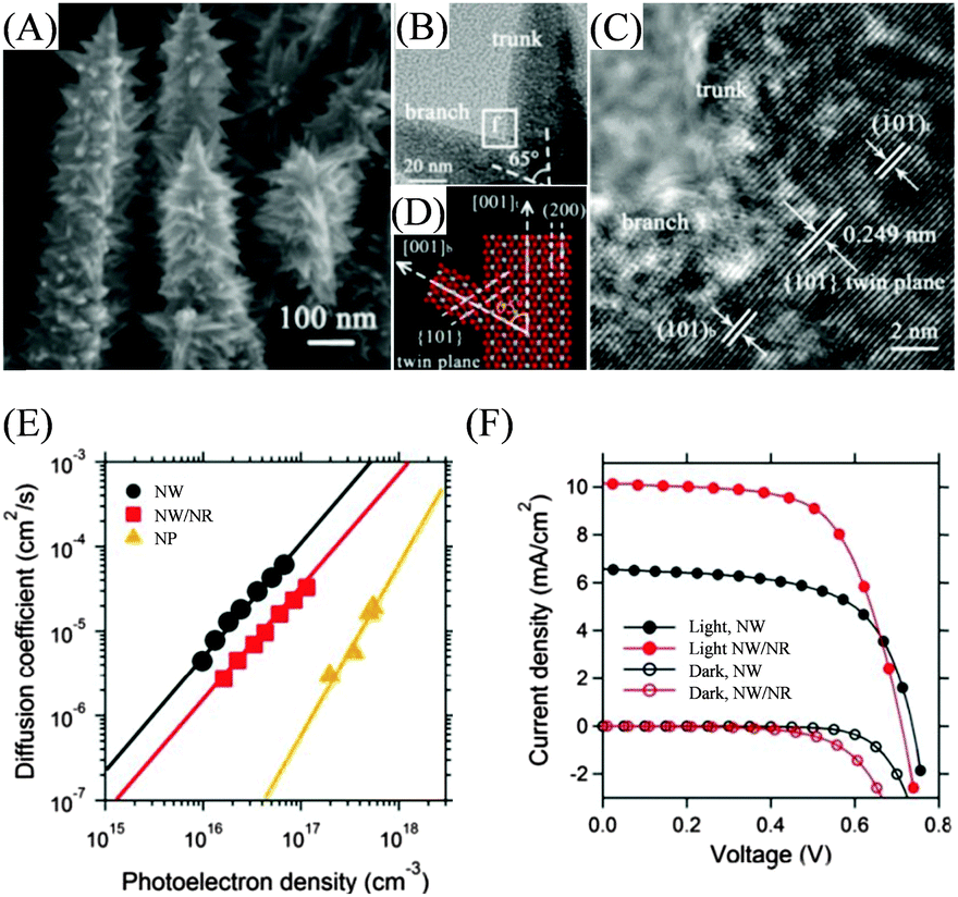 | ||
| Fig. 12 Single-crystalline TiO2 NW/NR nanostructure as a DSSC photoelectrode. (A) SEM, (B) TEM and (C) HRTEM images of the single-crystalline NW/NR nanostructure. (D) Schematic atomistic structure profile along the [010] zone axis of the trunk displayed in panel (C). (E) Electron diffusion coefficients (Dn) as a function of the photoelectron density for NW, single-crystalline NW/NR and NP film-based DSSCs. (F) J–V curves of the single-crystal NW/NR and NW-based DSSCs. Reproduced with permission from ref. 113. | ||
5. Conclusion and outlook
To sum up, hierarchical nanostructures of metal oxides have shown the expected advantages over the NP film and nanoarray counterparts in PEC solar energy conversion systems (water splitting and DSSC systems). In the water splitting system, a high performance photoelectrode needs to have both high light absorptivity and efficient charge separation/transport. For hierarchical nanostructures, the increased specific surface area due to the small size branches creates many more charge separation sites than in the nanoarray counterpart. In addition, the nanoarray trunk not only affords rapid charge transport but also enhances the light scattering capacity in comparison with the NP films. As a result, hierarchical nanostructures usually exhibit a superior performance to the NP and nanoarray counterparts. As learned from the high performance hierarchical nanostructure photoelectrodes, the trunks should have a single-crystalline structure or a polycrystalline structure with few high angle grain boundaries for fluent charge transport. Besides, the branch size should be sufficiently small to favor charge separation. Ideally, eliminating the grain boundaries between the trunk and branches to give a single-crystalline structure should be a very promising strategy.In the DSSC system, the metal oxides play the dual roles of supporting dye molecules and transporting the injected photoinduced electrons from the dye molecules. The earlier reported hierarchical nanostructure usually exhibited lower performance than the NP counterparts due to their considerably smaller specific surface area for dye deposition. However, the multi-level hierarchical nanostructures developed in recent years have largely solved this problem. Specifically, by introducing high-level and much smaller branches into the hierarchical nanostructures, one could significantly increase the specific surface area. In addition, hierarchical spherical aggregates have successfully promoted the cell efficiency to a record certified value by enlarging the surface area, improving charge transport and enhancing the light scattering capacity. Furthermore, hierarchical nanostructures have proved to be superior for constructing ssDSSCs because the well-aligned nanoarray trunks favor penetration into the solid-state electrolyte to afford excellent interface contact and charge separation. In a way similar to the water splitting system, a single-crystalline hierarchical nanostructure is a highly desirable candidate for DSSCs.
Clearly, there is still much room for further development of hierarchical nanostructure photoelectrodes. In particular, we foresee future developments in the following directions for both water splitting and DSSC systems. (1) Passivating surface states on hierarchical nanostructures. Small size branches usually induce higher surface state density, which not only increases charge recombination pathways but also suppresses charge transport rates by trapping/detrapping events. Therefore, it is necessary to passivate the surface states by depositing a thin oxide nanolayer (such as Al2O3, MgO2 and ZrO2) on the surface of hierarchical nanostructures. (2) Increasing carrier concentrations by doping the hierarchical nanostructure. Doping metal oxide hierarchical nanostructures will increase the carrier concentration and effectively increase the conductivity, while the increase in band bending will also favor charge separation at the surfaces. (3) Forming heterojunctions between the trunks and the branches. An appropriate energetic gradient formed by the heterojunction at the trunk/branch interface will favor charge separation, while the higher CB position of the branch oxides will decrease the recombination of injected electrons with the electrolyte. (4) Introducing 3D conducting substrates into the hierarchical nanostructure. A 3D conducting substrate (ITO or FTO glasses) will reduce the trunk length to improve the charge transport rate and collection efficiency, which will especially benefit metal oxides with a short carrier diffusion length.
Acknowledgements
This work was supported by the HK-RGC General Research Funds (GRF no. HKUST 606511) and the HK Innovation and Technology Fund (ITS/004/14).Notes and references
- W. Chen, Y. Qiu and S. Yang, Branched ZnO nanostructures as building blocks of photoelectrodes for efficient solar energy conversion, Phys. Chem. Chem. Phys., 2012, 14, 10872–10881 RSC.
- M. A. Butler and D. S. Ginley, Principles of photoelectrochemical, solar energy conversion, J. Mater. Sci., 1980, 15, 1–19 CrossRef CAS.
- R. Memming, Solar energy conversion by photoelectrochemical processes, Electrochim. Acta, 1980, 25, 77–88 CrossRef CAS.
- A. J. Bard, Design of semiconductor photoelectrochemical systems for solar energy conversion, J. Phys. Chem., 1982, 86, 172–177 CrossRef CAS.
- R. Memming, Photoelectrochemical solar energy conversion, in Electrochemistry II, in Top. Curr. Chem., ed. E. Steckhan, SpringerBerlin Heidelberg, 1988, vol. 143, pp. 79–112 Search PubMed.
- P. V. Kamat, Meeting the Clean Energy Demand: Nanostructure Architectures for Solar Energy Conversion, J. Phys. Chem. C, 2007, 111, 2834–2860 CAS.
- M. Gratzel, Photoelectrochemical cells, Nature, 2001, 414, 338–344 CrossRef CAS PubMed.
- M. G. Walter, E. L. Warren, J. R. McKone, S. W. Boettcher, Q. Mi, E. A. Santori and N. S. Lewis, Solar water splitting cells, Chem. Rev., 2010, 110, 6446–6473 CrossRef CAS PubMed.
- X. Wang, C. Liow, D. Qi, B. Zhu, W. R. Leow, H. Wang, C. Xue, X. Chen and S. Li, Programmable Photo-Electrochemical Hydrogen Evolution Based on Multi-Segmented CdS-Au Nanorod Arrays, Adv. Mater., 2014, 26, 3506–3512 CrossRef CAS PubMed.
- X. Wang, C. Liow, A. Bisht, X. Liu, T. C. Sum, X. Chen and S. Li, Engineering Interfacial Photo-Induced Charge Transfer Based on Nanobamboo Array Architecture for Efficient Solar-to-Chemical Energy Conversion, Adv. Mater., 2015, 27, 2207–2214 CrossRef CAS PubMed.
- B. O'Regan and M. Gratzel, A low-cost, high-efficiency solar cell based on dye-sensitized colloidal TiO2 films, Nature, 1991, 353, 737–740 CrossRef.
- A. Hagfeldt, G. Boschloo, L. Sun, L. Kloo and H. Pettersson, Dye-Sensitized Solar Cells, Chem. Rev., 2010, 110, 6595–6663 CrossRef CAS PubMed.
- H. G. Park and J. K. Holt, Recent advances in nanoelectrode architecture for photochemical hydrogen production, Energy Environ. Sci., 2010, 3, 1028–1036 CAS.
- A. Kudo and Y. Miseki, Heterogeneous photocatalyst materials for water splitting, Chem. Soc. Rev., 2009, 38, 253–278 RSC.
- A. B. Martinson, T. W. Hamann, M. J. Pellin and J. T. Hupp, New architectures for dye-sensitized solar cells, Chemistry, 2008, 14, 4458–4467 CrossRef CAS PubMed.
- J. Van de Lagemaat and A. Frank, Effect of the surface-state distribution on electron transport in dye-sensitized TiO2 solar cells: Nonlinear electron-transport kinetics, J. Phys. Chem. B, 2000, 104, 4292–4294 CrossRef CAS.
- J. Bisquert, Physical electrochemistry of nanostructured devices, Phys. Chem. Chem. Phys., 2008, 10, 49–72 RSC.
- W. Q. Wu, Y. F. Xu, C. Y. Su and D. B. Kuang, Ultra-long anatase TiO2 nanowire arrays with multi-layered configuration on FTO glass for high-efficiency dye-sensitized solar cells, Energy Environ. Sci., 2014, 7, 644–649 CAS.
- X. Feng, K. Shankar, O. K. Varghese, M. Paulose, T. J. Latempa and C. A. Grimes, Vertically aligned single crystal TiO2 nanowire arrays grown directly on transparent conducting oxide coated glass: synthesis details and applications, Nano Lett., 2008, 8, 3781–3786 CrossRef CAS PubMed.
- I. S. Cho, M. Logar, C. H. Lee, L. Cai, F. B. Prinz and X. Zheng, Rapid and controllable flame reduction of TiO2 nanowires for enhanced solar water-splitting, Nano Lett., 2014, 14, 24–31 CrossRef CAS PubMed.
- M. Law, L. E. Greene, J. C. Johnson, R. Saykally and P. Yang, Nanowire dye-sensitized solar cells, Nat. Mater., 2005, 4, 455–459 CrossRef CAS PubMed.
- H. N. Chen, L. Q. Zhu, M. Wang, H. C. Liu and W. P. Li, Wire-shaped quantum dots-sensitized solar cells based on nanosheets and nanowires, Nanotechnology, 2011, 22, 475402 CrossRef PubMed.
- H. N. Chen, L. Q. Zhu, H. C. Liu and W. P. Li, Growth of ZnO nanowires on fibers for one-dimensional flexible quantum dot-sensitized solar cells, Nanotechnology, 2012, 23, 075402 CrossRef PubMed.
- B. Liu and E. S. Aydil, Growth of Oriented Single-Crystalline Rutile TiO2 Nanorods on Transparent Conducting Substrates for Dye-Sensitized Solar Cells, J. Am. Chem. Soc., 2009, 131, 3985–3990 CrossRef CAS PubMed.
- E. Enache-Pommer, B. Liu and E. S. Aydil, Electron transport and recombination in dye-sensitized solar cells made from single-crystal rutile TiO2 nanowires, Phys. Chem. Chem. Phys., 2009, 11, 9648–9652 RSC.
- A. Wolcott, W. A. Smith, T. R. Kuykendall, Y. Zhao and J. Z. Zhang, Photoelectrochemical water splitting using dense and aligned TiO2 nanorod arrays, Small, 2009, 5, 104–111 CrossRef CAS PubMed.
- H. Chen, Z. Wei, K. Yan, Y. Bai and S. Yang, Unveiling Two Electron-Transport Modes in Oxygen-Deficient TiO2 Nanowires and Their Influence on Photoelectrochemical Operation, J. Phys. Chem. Lett., 2014, 5, 2890–2896 CrossRef CAS PubMed.
- Q. Kang, J. Cao, Y. Zhang, L. Liu, H. Xu and J. Ye, Reduced TiO2 nanotube arrays for photoelectrochemical water splitting, J. Mater. Chem. A, 2013, 1, 5766 CAS.
- P. Roy, S. Berger and P. Schmuki, TiO2 Nanotubes: Synthesis and Applications, Angew. Chem., Int. Ed., 2011, 50, 2904–2939 CrossRef CAS PubMed.
- A. B. F. Martinson, M. S. Góes, F. Fabregat-Santiago, J. Bisquert, M. J. Pellin and J. T. Hupp, Electron Transport in Dye-Sensitized Solar Cells Based on ZnO Nanotubes: Evidence for Highly Efficient Charge Collection and Exceptionally Rapid Dynamics†, J. Phys. Chem. A, 2009, 113, 4015–4021 CrossRef CAS PubMed.
- K. Zhu, N. R. Neale, A. Miedaner and A. J. Frank, Enhanced Charge-Collection Efficiencies and Light Scattering in Dye-Sensitized Solar Cells Using Oriented TiO2 Nanotubes Arrays, Nano Lett., 2007, 7, 69–74 CrossRef CAS PubMed.
- O. K. Varghese, M. Paulose and C. A. Grimes, Long vertically aligned titania nanotubes on transparent conducting oxide for highly efficient solar cells, Nat. Nanotechnol., 2009, 4, 592–597 CrossRef CAS PubMed.
- H. N. Chen, W. P. Li, H. C. Liu and L. Q. Zhu, CdS quantum dots sensitized single- and multi-layer porous ZnO nanosheets for quantum dots-sensitized solar cells, Electrochem. Commun., 2011, 13, 331–334 CrossRef CAS.
- Q. Hou, L. Q. Zhu, H. N. Chen, H. C. Liu and W. P. Li, Growth of flower-like porous ZnO nanosheets by electrodeposition with Zn-5(OH)(8)(NO3)(2)center dot 2H(2)O as precursor, Electrochim. Acta, 2012, 78, 55–64 CrossRef CAS.
- H. N. Chen, L. Q. Zhu, Q. Hou, H. C. Liu and W. P. Li, Hollow TiO2 Porous Nanosheets: Transformation from ZnO Porous Nanosheets and Application in Photoelectrochemical Cells, ChemSusChem, 2013, 6, 983–988 CrossRef CAS PubMed.
- H. N. Chen, L. Q. Zhu, H. C. Liu and W. P. Li, Zn-5(OH)(8)Cl-2 center dot H2O-based quantum dots-sensitized solar cells: A common corrosion product enhances the performance of photoelectrochemical cells, Electrochim. Acta, 2013, 105, 289–298 CrossRef CAS.
- Q. Hou, L. Q. Zhu, H. N. Chen, H. C. Liu and W. P. Li, Highly regular and ultra-thin porous ZnO nanosheets: An indirect electrodeposition method using acetate-containing precursor and their application in quantum dots-sensitized solar cells, Electrochim. Acta, 2013, 94, 72–79 CrossRef CAS.
- X. Wang, Z. Li, J. Shi and Y. Yu, One-Dimensional Titanium Dioxide Nanomaterials: Nanowires, Nanorods, and Nanobelts, Chem. Rev., 2014, 114, 9346–9384 CrossRef CAS PubMed.
- Q. Zhang and G. Cao, Nanostructured photoelectrodes for dye-sensitized solar cells, Nano Today, 2011, 6, 91–109 CrossRef CAS.
- Q. Zhang and G. Cao, Hierarchically structured photoelectrodes for dye-sensitized solar cells, J. Mater. Chem., 2011, 21, 6769–6774 RSC.
- H.-Y. Chen, D.-B. Kuang and C.-Y. Su, Hierarchically micro/nanostructured photoanode materials for dye-sensitized solar cells, J. Mater. Chem., 2012, 22, 15475–15489 RSC.
- C. Cheng and H. J. Fan, Branched nanowires: Synthesis and energy applications, Nano Today, 2012, 7, 327–343 CrossRef CAS.
- B. Nikoobakht, X. Wang, A. Herzing and J. Shi, Scalable synthesis and device integration of self-registered one-dimensional zinc oxide nanostructures and related materials, Chem. Soc. Rev., 2013, 42, 342–365 RSC.
- F. E. Osterloh, Inorganic nanostructures for photoelectrochemical and photocatalytic water splitting, Chem. Soc. Rev., 2013, 42, 2294–2320 RSC.
- Z.-F. Huang, L. Pan, J.-J. Zou, X. Zhang and L. Wang, Nanostructured Bismuth Vanadate-Based Materials for Solar-Energy-Driven Water Oxidation: A Review on Recent Progress, Nanoscale, 2014, 6, 14044–14063 RSC.
- Z. Ren, Y. Guo, C.-H. Liu and P.-X. Gao, Hierarchically Nanostructured Materials for Sustainable Environmental Applications, Front. Chem., 2013, 1, 18 Search PubMed.
- Q. Zhang, E. Uchaker, S. L. Candelaria and G. Cao, Nanomaterials for energy conversion and storage, Chem. Soc. Rev., 2013, 42, 3127–3171 RSC.
- Q. Zhang, K. Park, J. Xi, D. Myers and G. Cao, Recent Progress in Dye-Sensitized Solar Cells Using Nanocrystallite Aggregates, Adv. Energy Mater., 2011, 1, 988–1001 CrossRef CAS.
- X. Xin, Dye-and quantum dot-sensitized solar cells based on nanostructured wide-bandgap semiconductors via an integrated experimental and modeling study, 2012 Search PubMed.
- Z. Yang, C. Y. Chen, P. Roy and H. T. Chang, Quantum dot-sensitized solar cells incorporating nanomaterials, Chem. Commun., 2011, 47, 9561–9571 RSC.
- J. Xu, Z. Chen, J. A. Zapien, C.-S. Lee and W. Zhang, Surface Engineering of ZnO Nanostructures for Semiconductor-Sensitized Solar Cells, Adv. Mater., 2014, 26, 5337–5367 CrossRef CAS PubMed.
- J. Tian and G. Cao, Control of Nanostructures and Interfaces of Metal Oxide Semiconductors for Quantum-Dots-Sensitized Solar Cells, J. Phys. Chem. Lett., 2015, 6, 1859–1869 CrossRef CAS PubMed.
- L. Forro, O. Chauvet, D. Emin, L. Zuppiroli, H. Berger and F. Lévy, High mobility n-type charge carriers in large single crystals of anatase (TiO2), J. Appl. Phys., 1994, 75, 633–635 CrossRef CAS.
- L. Dloczik, O. Ileperuma, I. Lauermann, L. M. Peter, E. A. Ponomarev, G. Redmond, N. J. Shaw and I. Uhlendorf, Dynamic Response of Dye-Sensitized Nanocrystalline Solar Cells: Characterization by Intensity-Modulated Photocurrent Spectroscopy, J. Phys. Chem. B, 1997, 101, 10281–10289 CrossRef CAS.
- A. C. Fisher, L. M. Peter, E. A. Ponomarev, A. B. Walker and K. G. U. Wijayantha, Intensity Dependence of the Back Reaction and Transport of Electrons in Dye-Sensitized Nanocrystalline TiO2 Solar Cells, J. Phys. Chem. B, 2000, 104, 949–958 CrossRef CAS.
- J. R. Jennings, A. Ghicov, L. M. Peter, P. Schmuki and A. B. Walker, Dye-Sensitized Solar Cells Based on Oriented TiO2 Nanotube Arrays: Transport, Trapping, and Transfer of Electrons, J. Am. Chem. Soc., 2008, 130, 13364–13372 CrossRef CAS PubMed.
- I. S. Cho, Z. Chen, A. J. Forman, D. R. Kim, P. M. Rao, T. F. Jaramillo and X. Zheng, Branched TiO(2) nanorods for photoelectrochemical hydrogen production, Nano Lett., 2011, 11, 4978–4984 CrossRef CAS PubMed.
- K. Sivula, F. Le Formal and M. Grätzel, Solar Water Splitting: Progress Using Hematite (α-Fe2O3) Photoelectrodes, ChemSusChem, 2011, 4, 432–449 CrossRef CAS PubMed.
- P. M. Rao, L. Cai, C. Liu, I. S. Cho, C. H. Lee, J. M. Weisse, P. Yang and X. Zheng, Simultaneously Efficient Light Absorption and Charge Separation in WO3/BiVO4 Core/Shell Nanowire Photoanode for Photoelectrochemical Water Oxidation, Nano Lett., 2014, 14, 1099–1105 CrossRef CAS PubMed.
- X. Sun, Q. Li, J. Jiang and Y. Mao, Morphology-tunable synthesis of ZnO nanoforest and its photoelectrochemical performance, Nanoscale, 2014, 6, 8769–8780 RSC.
- Y. Qiu and S. Yang, ZnO Nanotetrapods: Controlled Vapor-Phase Synthesis and Application for Humidity Sensing, Adv. Funct. Mater., 2007, 17, 1345–1352 CrossRef CAS.
- Z. Zhu, J. Qiu, K. Yan and S. Yang, Building High-Efficiency CdS/CdSe-Sensitized Solar Cells with a Hierarchically Branched Double-Layer Architecture, ACS Appl. Mater. Interfaces, 2013, 5, 4000–4005 CAS.
- K. Yan, L. Zhang, J. Qiu, Y. Qiu, Z. Zhu, J. Wang and S. Yang, A quasi-quantum well sensitized solar cell with accelerated charge separation and collection, J. Am. Chem. Soc., 2013, 135, 9531–9539 CrossRef CAS PubMed.
- W. Chen, H. Zhang, I. M. Hsing and S. Yang, A new photoanode architecture of dye sensitized solar cell based on ZnO nanotetrapods with no need for calcination, Electrochem. Commun., 2009, 11, 1057–1060 CrossRef CAS.
- W. Chen, Y. Qiu and S. Yang, A new ZnO nanotetrapods/SnO2 nanoparticles composite photoanode for high efficiency flexible dye-sensitized solar cells, Phys. Chem. Chem. Phys., 2010, 12, 9494–9501 RSC.
- W. Chen, Y. Qiu, Y. Zhong, K. S. Wong and S. Yang, High-Efficiency Dye-Sensitized Solar Cells Based on the Composite Photoanodes of SnO2 Nanoparticles/ZnO Nanotetrapods, J. Phys. Chem. A, 2010, 114, 3127–3138 CrossRef CAS PubMed.
- Y. Qiu, K. Yan, H. Deng and S. Yang, Secondary branching and nitrogen doping of ZnO nanotetrapods: building a highly active network for photoelectrochemical water splitting, Nano Lett., 2012, 12, 407–413 CrossRef CAS PubMed.
- C. T. Wu, W. P. Liao and J. J. Wu, Three-dimensional ZnO nanodendrite/nanoparticle composite solar cells, J. Mater. Chem., 2011, 21, 2871–2876 RSC.
- Y. Qiu, S.-F. Leung, Z. Wei, Q. Lin, X. Zheng, Y. Zhang, Z. Fan and S. Yang, Enhanced Charge Collection for Splitting of Water Enabled by an Engineered Three-Dimensional Nanospike Array, J. Phys. Chem. C, 2014, 118, 22465–22472 CAS.
- Y. Yue, X. Yang, Y. Wu, N. T. Salim, A. Islam, T. Noda and L. Han, Selective Deposition of Insulating Metal Oxide in Perovskite Solar Cells with Enhanced Device Performance, ChemSusChem, 2015, 8, 2625–2629 CrossRef CAS PubMed.
- H. Chen, Z. Wei, K. Yan, Y. Yi, J. Wang and S. Yang, Liquid phase deposition of TiO 2 nanolayer affords CH 3 NH 3 PbI 3/nanocarbon solar cells with high open-circuit voltage, Faraday Discuss., 2014, 176, 271–286 RSC.
- L. A. Marusak, R. Messier and W. B. White, Optical absorption spectrum of hematite, αFe2O3 near IR to UV, J. Phys. Chem. Solids, 1980, 41, 981–984 CrossRef CAS.
- A. Kay, I. Cesar and M. Grätzel, New Benchmark for Water Photooxidation by Nanostructured α-Fe2O3 Films, J. Am. Chem. Soc., 2006, 128, 15714–15721 CrossRef CAS PubMed.
- S. D. Tilley, M. Cornuz, K. Sivula and M. Grätzel, Light-Induced Water Splitting with Hematite: Improved Nanostructure and Iridium Oxide Catalysis, Angew. Chem., Int. Ed., 2010, 49, 6405–6408 CrossRef CAS PubMed.
- S. C. Warren, K. Voitchovsky, H. Dotan, C. M. Leroy, M. Cornuz, F. Stellacci, C. Hebert, A. Rothschild and M. Gratzel, Identifying champion nanostructures for solar water-splitting, Nat. Mater., 2013, 12, 842–849 CrossRef CAS PubMed.
- H. Chen, Z. Wei, K. Yan, Y. Bai, Z. Zhu, T. Zhang and S. Yang, Epitaxial Growth of ZnO Nanodisks with Large Exposed Polar Facets on Nanowire Arrays for Promoting Photoelectrochemical Water Splitting, Small, 2014, 10, 4760–4769 CrossRef CAS PubMed.
- H. Wang, Y. S. Bai, Q. O. Wu, W. Zhou, H. Zhang, J. H. Li and L. Guo, Rutile TiO2 nano-branched arrays on FTO for dye-sensitized solar cells, Phys. Chem. Chem. Phys., 2011, 13, 6977–6982 Search PubMed.
- D. Lee, Y. Rho, F. I. Allen, A. M. Minor, S. H. Ko and C. P. Grigoropoulos, Synthesis of hierarchical TiO2 nanowires with densely-packed and omnidirectional branches, Nanoscale, 2013, 5, 11147–11152 RSC.
- L. Chu, L. Li, J. Su, F. Tu, N. Liu and Y. Gao, A General Method for Preparing Anatase TiO2 Treelike-Nanoarrays on Various Metal Wires for Fiber Dye-Sensitized Solar Cells, Sci. Rep., 2014, 4, 4020 Search PubMed.
- F. Shao, J. Sun, L. Gao, S. Yang and J. Luo, Forest-like TiO2 hierarchical structures for efficient dye-sensitized solar cells, J. Mater. Chem., 2012, 22, 6824–6830 RSC.
- M. Ye, D. Zheng, M. Lv, C. Chen, C. Lin and Z. Lin, Hierarchically structured nanotubes for highly efficient dye-sensitized solar cells, Adv. Mater., 2013, 25, 3039–3044 CrossRef CAS PubMed.
- P. Roy, D. Kim, I. Paramasivam and P. Schmuki, Improved efficiency of TiO2 nanotubes in dye sensitized solar cells by decoration with TiO2 nanoparticles, Electrochem. Commun., 2009, 11, 1001–1004 CrossRef CAS.
- W. Guo, D. Zheng, M. Lu, C.-J. Lin and Z. L. Wang, Branched TiO2 Nanorods Covered with TiO2 Nanosheets for Harvesting Solar Energies in Dye-Sensitized Solar Cells, ECS Trans., 2011, 41, 103–109 CAS.
- C. Y. Jiang, X. W. Sun, G. Q. Lo, D. L. Kwong and J. X. Wang, Improved dye-sensitized solar cells with a ZnO-nanoflower photoanode, Appl. Phys. Lett., 2007, 90, 263501 CrossRef.
- S. H. Ko, D. Lee, H. W. Kang, K. H. Nam, J. Y. Yeo, S. J. Hong, C. P. Grigoropoulos and H. J. Sung, Nanoforest of hydrothermally grown hierarchical ZnO nanowires for a high efficiency dye-sensitized solar cell, Nano Lett., 2011, 11, 666–671 CrossRef CAS PubMed.
- M. McCune, W. Zhang and Y. Deng, High efficiency dye-sensitized solar cells based on three-dimensional multilayered ZnO nanowire arrays with “caterpillar-like” structure, Nano Lett., 2012, 12, 3656–3662 CrossRef CAS PubMed.
- H. M. Cheng, W. H. Chiu, C. H. Lee, S. Y. Tsai and W. F. Hsieh, Formation of Branched ZnO Nanowires from Solvothermal Method and Dye-Sensitized Solar Cells Applications, J. Phys. Chem. C, 2008, 112, 16359–16364 CAS.
- F. Xu, M. Dai, Y. Lu and L. Sun, Hierarchical ZnO Nanowire–Nanosheet Architectures for High Power Conversion Efficiency in Dye-Sensitized Solar Cells, J. Phys. Chem. C, 2010, 114, 2776–2782 CAS.
- J. Qiu, M. Guo and X. Wang, Electrodeposition of Hierarchical ZnO Nanorod-Nanosheet Structures and Their Applications in Dye-Sensitized Solar Cells, ACS Appl. Mater. Interfaces, 2011, 3, 2358–2367 CAS.
- W. T. Jiang, C. T. Wu, Y. H. Sung and J. J. Wu, Room-temperature fast construction of outperformed ZnO nanoarchitectures on nanowire-array templates for dye-sensitized solar cells, ACS Appl. Mater. Interfaces, 2013, 5, 911–917 CAS.
- H. Kim and K. Yong, A highly efficient light capturing 2D (nanosheet)-1D (nanorod) combined hierarchical ZnO nanostructure for efficient quantum dot sensitized solar cells, Phys. Chem. Chem. Phys., 2013, 15, 2109–2116 RSC.
- M. Ye, X. Xin, C. Lin and Z. Lin, High Efficiency Dye-Sensitized Solar Cells Based on Hierarchically Structured Nanotubes, Nano Lett., 2011, 11, 3214–3220 CrossRef CAS PubMed.
- W.-Q. Wu, H.-S. Rao, H.-L. Feng, H.-Y. Chen, D.-B. Kuang and C.-Y. Su, A family of vertically aligned nanowires with smooth, hierarchical and hyperbranched architectures for efficient energy conversion, Nano Energy, 2014, 9, 15–24 CrossRef CAS.
- X. Dou, D. Sabba, N. Mathews, L. H. Wong, Y. M. Lam and S. Mhaisalkar, Hydrothermal Synthesis of High Electron Mobility Zn-doped SnO2 Nanoflowers as Photoanode Material for Efficient Dye-Sensitized Solar Cells, Chem. Mater., 2011, 23, 3938–3945 CrossRef CAS.
- Q. Zhang, C. S. Dandeneau, X. Zhou and G. Cao, ZnO Nanostructures for Dye-Sensitized Solar Cells, Adv. Mater., 2009, 21, 4087–4108 CrossRef CAS.
- C. Yasuo, I. Ashraful, W. Yuki, K. Ryoichi, K. Naoki and H. Liyuan, Dye-Sensitized Solar Cells with Conversion Efficiency of 11.1%, Jpn. J. Appl. Phys., 2006, 45, L638 CrossRef.
- A. Yella, H.-W. Lee, H. N. Tsao, C. Yi, A. K. Chandiran, M. K. Nazeeruddin, E. W.-G. Diau, C.-Y. Yeh, S. M. Zakeeruddin and M. Grätzel, Porphyrin-Sensitized Solar Cells with Cobalt(II/III)–Based Redox Electrolyte Exceed 12 Percent Efficiency, Science, 2011, 334, 629–634 CrossRef CAS PubMed.
- S. Mathew, A. Yella, P. Gao, R. Humphry-Baker, F. E. CurchodBasile, N. Ashari-Astani, I. Tavernelli, U. Rothlisberger, K. NazeeruddinMd and M. Grätzel, Dye-sensitized solar cells with 13% efficiency achieved through the molecular engineering of porphyrin sensitizers, Nat. Chem., 2014, 6, 242–247 CrossRef CAS PubMed.
- W.-Q. Wu, H.-L. Feng, H.-S. Rao, Y.-F. Xu, D.-B. Kuang and C.-Y. Su, Maximizing omnidirectional light harvesting in metal oxide hyperbranched array architectures, Nat. Commun., 2014, 5, 3968 CAS.
- W.-Q. Wu, Y.-F. Xu, H.-S. Rao, C.-Y. Su and D.-B. Kuang, Multistack Integration of Three-Dimensional Hyperbranched Anatase Titania Architectures for High-Efficiency Dye-Sensitized Solar Cells, J. Am. Chem. Soc., 2014, 136, 6437–6445 CrossRef CAS PubMed.
- T. P. Chou, Q. Zhang, G. E. Fryxell and G. Z. Cao, Hierarchically Structured ZnO Film for Dye-Sensitized Solar Cells with Enhanced Energy Conversion Efficiency, Adv. Mater., 2007, 19, 2588–2592 CrossRef CAS.
- Q. Zhang, T. P. Chou, B. Russo, S. A. Jenekhe and G. Cao, Aggregation of ZnO nanocrystallites for high conversion efficiency in dye-sensitized solar cells, Angew. Chem., 2008, 47, 2402–2406 CrossRef CAS PubMed.
- K. Park, Q. Zhang, B. B. Garcia, X. Zhou, Y. H. Jeong and G. Cao, Effect of an ultrathin TiO(2) layer coated on submicrometer-sized ZnO nanocrystallite aggregates by atomic layer deposition on the performance of dye-sensitized solar cells, Adv. Mater., 2010, 22, 2329–2332 CrossRef CAS PubMed.
- N. Memarian, I. Concina, A. Braga, S. M. Rozati, A. Vomiero and G. Sberveglieri, Hierarchically Assembled ZnO Nanocrystallites for High-Efficiency Dye-Sensitized Solar Cells, Angew. Chem., Int. Ed., 2011, 50, 12321–12325 CrossRef CAS PubMed.
- D. Chen, F. Huang, Y.-B. Cheng and R. A. Caruso, Mesoporous Anatase TiO2Beads with High Surface Areas and Controllable Pore Sizes: A Superior Candidate for High-Performance Dye-Sensitized Solar Cells, Adv. Mater., 2009, 21, 2206–2210 CrossRef CAS.
- D. Chen, L. Cao, F. Huang, P. Imperia, Y. B. Cheng and R. A. Caruso, Synthesis of monodisperse mesoporous titania beads with controllable diameter, high surface areas, and variable pore diameters (14–23 nm), J. Am. Chem. Soc., 2010, 132, 4438–4444 CrossRef CAS PubMed.
- F. Huang, D. Chen, X. L. Zhang, R. A. Caruso and Y.-B. Cheng, Dual-Function Scattering Layer of Submicrometer-Sized Mesoporous TiO2 Beads for High-Efficiency Dye-Sensitized Solar Cells, Adv. Funct. Mater., 2010, 20, 1301–1305 CrossRef CAS.
- F. Sauvage, D. Chen, P. Comte, F. Huang, L.-P. Heiniger, Y.-B. Cheng, R. A. Caruso and M. Graetzel, Dye-Sensitized Solar Cells Employing a Single Film of Mesoporous TiO2 Beads Achieve Power Conversion Efficiencies Over 10%, ACS Nano, 2010, 4, 4420–4425 CrossRef CAS PubMed.
- D. H. Chen and R. A. Caruso, Recent Progress in the Synthesis of Spherical Titania Nanostructures and Their Applications, Adv. Funct. Mater., 2013, 23, 1356–1374 CrossRef CAS.
- K. Yan, Y. Qiu, W. Chen, M. Zhang and S. Yang, A double layered photoanode made of highly crystalline TiO2 nanooctahedra and agglutinated mesoporous TiO2 microspheres for high efficiency dye sensitized solar cells, Energy Environ. Sci., 2011, 4, 2168 CAS.
- Y. Liu, R. Che, G. Chen, J. Fan, Z. Sun, Z. Wu, M. Wang, B. Li, J. Wei, Y. Wei, G. Wang, G. Guan, A. A. Elzatahry, A. A. Bagabas, A. M. Al-Enizi, Y. Deng, H. Peng and D. Zhao, Radially oriented mesoporous TiO2 microspheres with single-crystal-like anatase walls for high-efficiency optoelectronic devices, 2015, vol. 1 Search PubMed.
- D. K. Roh, W. S. Chi, H. Jeon, S. J. Kim and J. H. Kim, High Efficiency Solid-State Dye-Sensitized Solar Cells Assembled with Hierarchical Anatase Pine Tree-like TiO2 Nanotubes, Adv. Funct. Mater., 2014, 24, 379–386 CrossRef CAS.
- X. Sheng, D. He, J. Yang, K. Zhu and X. Feng, Oriented assembled TiO2 hierarchical nanowire arrays with fast electron transport properties, Nano Lett., 2014, 14, 1848–1852 CrossRef CAS PubMed.
| This journal is © The Royal Society of Chemistry 2016 |