
 Open Access Article
 This Open Access Article is licensed under a
 Creative Commons Attribution 3.0 Unported Licence
Carrier trapping and recombination: the role of defect physics in enhancing the open circuit voltage of metal halide perovskite solar cells†
Tomas
Leijtens
*ab,
Giles E.
Eperon
c,
Alex J.
Barker
a,
Giulia
Grancini
a,
Wei
Zhang‡
c,
James M.
Ball
a,
Ajay Ram Srimath
Kandada
a,
Henry J.
Snaith
c and
Annamaria
Petrozza
*a
aCenter for Nano Science and Technology@Polimi, Istituto Italiano di Tecnologia, via Giovanni Pascoli 70/3, 20133, Milan, Italy. E-mail: Annamaria.Petrozza@iit.it
bDepartment of Materials Science and Engineering, Stanford University, Stanford, CA 94305, USA. E-mail: leijtens@stanford.edu
cUniversity of Oxford, Clarendon Laboratory, Parks Road, Oxford, OX1 3PU, UK
First published on 9th September 2016
Abstract
One of the greatest attributes of metal halide perovskite solar cells is their surprisingly low loss in potential between bandgap and open-circuit voltage, despite the fact that they suffer from a non-negligible density of sub gap defect states. Here, we use a combination of transient and steady state photocurrent and absorption spectroscopy to show that CH3NH3PbI3 films exhibit a broad distribution of electron traps. We show that the trapped electrons recombine with free holes unexpectedly slowly, on microsecond time scales, relaxing the limit on obtainable open-circuit voltage (VOC) under trap-mediated recombination conditions. We find that the observed VOCs in such perovskite solar cells can only be rationalized by considering the slow trap mediated recombination mechanism identified in this work. Our results suggest that existing processing routes may be good enough to enable open circuit voltages approaching 1.3 V in ideal devices with perfect contacts.
Broader contextIt is now well established that the primary optoelectronic properties of perovskite-halides meet many of the requirements for high-efficiency technology. However, many of the details governing the device physics remain under debate. Of particular importance is the understanding of the effects of defects on the properties of devices. Indeed, given the simple processability of these materials, one could expect a non-negligible level of unintentional structural and chemical defects within the semiconductor. In more established semiconductors, such as Si, the understanding and control of defects has been a cornerstone of their successful development. In perovskite-halides several studies have attempted to explain their favourable properties by suggesting that most defect species are energetically shallow, minimising their impact in loss mechanisms. However, their light-emitting properties are far from ideal, implying that deep levels are also important. Thus, it seems likely that defects in perovskite-halides are one of the significant remaining material characteristics that underpin device operation, guiding further progress towards reaching optimal power conversion efficiencies. |
Introduction
Metal halide perovskite solar cells owe their rapid increase of power conversion efficiencies over 22%1,2 to several key properties. They benefit from low exciton binding energies,3,4 high ambipolar mobilities,5–7 high absorption cross-sections,8 and long carrier lifetimes.5,9,10 These properties have allowed this class of materials to function effectively as not just photovoltaic devices, but also as light emitting diodes (LEDs) and optically pumped lasers.11–13 Still, the materials are known to suffer from a significant density of sub gap states that should induce non-negligible recombination losses.9,10,14,15 Extensive time resolved photoluminescence and terahertz spectroscopy on the most commonly employed CH3NH3PbI3 perovskite have shown that, at solar fluences, the photo-carrier dynamics are limited by a monomolecular trapping process, while the radiative bimolecular recombination process is surprisingly slow and hence only dominates at high excitation densities.7,9,10,16 While it is accepted that carrier trapping plays a dominant role in perovskite photo-carrier dynamics at solar fluences, the nature of the traps and the recombination pathway has remained unexplored.Generally, carrier trapping into deep sub gap states is considered to lead to rapid non-radiative recombination which severely limits the quasi-Fermi level splitting of the materials, and hence the photovoltage of the solar cells. This follows the Shockley Reed Hall (SRH) framework, where recombination occurs through a state within the forbidden band of the semiconductor. The SRH behavior can be categorized by two distinct regimes where the semiconductor is either doped or closer to intrinsic. In a highly doped semiconductor, trapping into a sub gap state leads to immediate annihilation by the many excess carriers of the opposite charge, while trapping into such a state does not necessarily lead to immediate recombination in a lightly or undoped material. The SRH model has generally been applied to highly doped silicon solar cells where trapping results in immediate recombination and hence the trapping lifetime of the minority carrier becomes the most relevant parameter.17 Indeed, SRH recombination has been generally proposed to dominate in lead halide semiconductors.7,10,17,18 Despite evidence that the perovskite layers are generally only lightly doped, previous works have primarily assumed that the recombination rate of the trapped electron or hole is the same as the trapping rate, and hence the trapping lifetime has been used to estimate both electron and hole diffusion lengths.6,7,19 With the reported sub-gap trap densities of around 1016 cm−3 and an effective trapping lifetime of about 100 ns,9,10 rapid trap mediated recombination would result in a severe limitation to attainable photovoltages of perovskite solar cells. Still, this relatively new technology boosts voltages already approaching 1.2 V,20,21 which is remarkably high for a semiconductor with a bandgap of only 1.6 eV. In the limit where all recombination is due to radiative band-to-band recombination the material should be able to achieve ideal VOCs of around 1.3 V,22 not much higher than what has been already experimentally obtained. This suggests that the sub gap states, thought to be almost unavoidable in a solution processed and low-temperature crystallized material, may not form highly detrimental recombination centers. Previous photoconductivity measurements led us to suggest that the carrier trapping process leads to a photodoping effect, which implies a long lived trapped species and associated long lived free carrier species.14 Such slow trap mediated recombination would allow for far greater Fermi level splitting and VOCs compared to the rapid trap mediated recombination where the trapped carriers recombine almost instantaneously with free carriers. Still, such a phenomenon has hitherto remained unexplored within the field of perovskite solar cells. While several photophysical models have been developed to explain photoluminescence decays,7,9,10 none has been extended to consider the recombination lifetimes of the trapped charge even though this may be one of the most relevant parameters to consider when it comes to determining how detrimental a given density of trap sites might be to the total recombination flux, quasi Fermi level splitting, and photovoltage in solar cells. Some important questions that remain to be addressed can be summarized as follows: (1) do the predominant defects act as electron or hole traps? (2) What is their energetic distribution? (3) How rapid is trap mediated recombination? (4) How does the effective carrier lifetime affect the theoretically obtainable VOCs of perovskite solar cells?
In this work, we directly monitor trapped electron–free hole recombination kinetics in metal halide perovskite films for the first time, establishing that CH3NH3PbI3 suffers from a significant and broad density of sub gap electron traps. Surprisingly, after an initial fast electron trapping process (100 ns lifetime), the trapped electrons slowly recombine with free holes on tens of μs timescales, thus deviating significantly from the expected rapid trap mediated recombination pathway. This results in a situation where most of the traps are filled at solar fluences allowing the solar cells to obtain improved photovoltages.
We finally address the implications to the theoretically obtainable VOCs in perovskite solar cells by using simple Fermi–Dirac statistics. If we account for the slow trapped charge recombination and associated trap filling we estimate maximum obtainable VOCs close to 1.3 V, about 150 mV higher than that expected for rapid trap mediated recombination—clearly more consistent with the experimental results.20,21 These findings shed light on the high photovoltages achieved for this system despite the inevitable presence of significant trap densities inherent in solution processed semiconductors.
Results and discussion
1. Nature and energetic distribution of trap sites
In order to firstly measure the trap energy distribution, we performed Fourier transform photocurrent spectroscopy on a perovskite layer with two lateral Ohmic contacts, which serves as a photoresistor. Any photocurrent collected upon sub gap excitation directly implies the presence of sub gap sites, and so this measurement allows us to obtain the energetic distribution of such states.The sample structure is shown in Fig. 1a, and the normalized photocurrent spectrum is shown in Fig. 1b. We used a gold/perovskite/gold structure (the perovskite deposition method for all measurements except where otherwise noted is the PbCl2 derived perovskite), which guarantees an Ohmic response limited by the semiconductor layer rather than the contacts (see Fig. S1, ESI†),23,24 applying a bias of 10 V over a channel of 4 mm. Since the device functions as a planar photodetector with symmetric contacts, we only require the presence of one free carrier to measure any photocurrent under an external applied bias.14 This allows us to detect transitions that result in only one free carrier. Consistent with previous reports of low Urbach energies we observe a sharp band edge onset in the photocurrent corresponding to an Urbach energy of 25 meV25 (Fig. 1), but also observe an additional broad tail with a distinct slope in the photocurrent extending from the band edge to the instrument limitation at almost 1.1 eV. This is direct evidence for the presence of a broad distribution of trap states down to at least 0.5 eV from either the valence or conduction band edge. Previous theoretical studies have focused on identifying distinct types of defects with discrete energy levels, with the most recent work suggesting that iodide interstitials are likely to manifest themselves as relatively deep electron traps.26–28 The shape of our sub gap photocurrent spectrum is not completely coherent with this scenario. It seems possible that the broad distribution of sub gap states could be due to an inhomogeneity in crystallinity and perhaps stoichiometry on the nano-to-micro scale, or even to the presence of multidimensional defects which have not yet been well studied.
 | ||
| Fig. 1 (a) Schematic of the symmetric laterally contacted device held under 10 V applied bias. (b) Normalized photocurrent spectral response of the device at an applied bias of 10 V; the device is encapsulated with an inert PMMA layer. (c) Photocurrent (10 V) as a function of intensity of an above gap (690 nm) excitation for devices covered by a hole accepting Spiro-OMeTAD, an electron accepting PCBM, or an inert PMMA layer. (d) Photocurrent (10 V) of the same devices as a function of fluence of a sub gap (850 nm) excitation. We point out that the fluence denoted in 1d is not equivalent to an absorbed fluence; the absorption cross-section at 850 nm is unknown and may be different for different samples. | ||
Having established that our material is suffering from the presence of a broad distribution of sub gap trap sites, we aim to determine whether this distribution is associated with electron or hole trapping, or both. Here, we measure the photocurrent from the same device architecture shown in Fig. 1a upon monochromatic excitation both above and below gaps. We compare the pristine perovskite covered by a thin layer of inert PMMA with the one covered by a thin hole accepting (Spiro-OMeTAD, referred to as Spiro) or electron accepting layer (PCBM).5 The perovskite is directly excited and the vast majority of the detected current comes from the carriers in the perovskite layer only (see S1, ESI†).14 We point out that the photocurrent measured here is proportional to the carrier densities and their mobilities. Under steady state illumination, the carrier density is determined by the carrier lifetime. This can be formally represented by eqn (1):29
| I ∝ q(n·μn + p·μp) = q(G·τn·μn + G·τp·μp) | (1) |
So far, the results suggest that the material suffers from a significant and broad density of sub gap electron traps, which limit effective long-range electron mobility. To relate the photocurrent response upon sub gap excitation observed in Fig. 1b to the behavior in Fig. 1c, we excited the samples using a sub gap excitation source (850 nm laser) and monitored the photocurrent. The results are plotted in Fig. 1d, and show that sub gap excitation leads to little to no detectable photocurrent (over three orders of magnitude lower than the neat samples) when a hole acceptor is placed on top of the samples. On the other hand, the presence of an electron acceptor has a similar effect as with the above gap illumination. This allows us to claim that deep electron traps are present, which can be directly populated by excitation from the valence band to yield trapped electrons and free holes. The free holes can be collected as a photocurrent in neat samples, but no photocurrent is collected in samples with the Spiro hole acceptor simply because there are only trapped electrons left in the film. The proposed mechanism is displayed in Scheme 1. It is worth noting that upon sub-gap excitation, in principle, one would expect the same photocurrent for PCBM and PMMA contacted thin films. Nevertheless in Fig. 1d we do notice a small deviation. We speculate that this may be due to a different chemical interaction between the interfaced materials which may cause the density, nature, distribution, and lifetime of trapped electrons to be different.
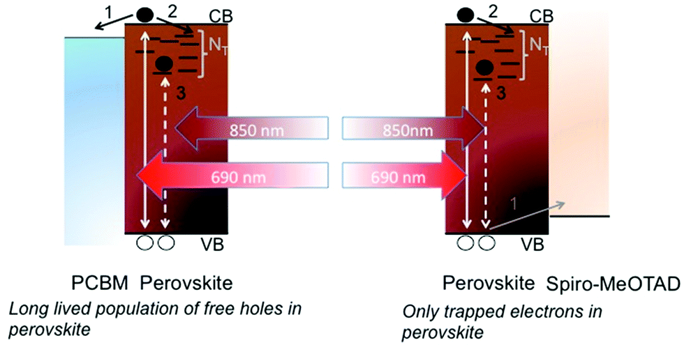 | ||
| Scheme 1 Schematic illustration of carrier dynamics upon above and below gap excitation when the perovskite is contacted by electron (PCBM) and hole (Spiro-MeOTAD) accepting layers. | ||
Note that in Fig. 1c the sublinear behavior for the electron-accepting sample suggests that recombination across the perovskite–PCBM interface has a charge density dependence, while this is not observed for the perovskite–Spiro interface. This is well in agreement with the scenario where free electrons in the PCBM and free holes in the perovskite recombine in the first case, while free holes in the Spiro will recombine with localized, trapped electrons in the perovskite in the second case.
2. Trap mediated recombination lifetimes and mechanism
In an effort to directly monitor the trapped electron lifetimes, we performed transient photocurrent measurements on the same samples used for the steady state photocurrent measurements, this time using a pulsed excitation analogous to that used in transient PL measurements rather than a steady state excitation. This measurement allows us to monitor the transient photoconductivity of the perovskite layer with various charge quenching layers, and thus directly probe the free carrier population as a function of time after excitation. Monitoring the photoconductivity rather than the photoluminescence means that we are not limited by the presence of radiative recombination but can monitor any free carrier. We start by performing an above gap fluence dependence with non-quenching samples (Fig. 2a). In the early stages (<1 μs) the decays become steeper for higher excitation densities as previously observed via photoluminescence spectroscopy when moving from monomolecular to bimolecular recombination regimes. Interestingly, we also observe an extremely slow component in the photoconductivity traces that makes up an increasingly large fraction of the decay as the excitation density is reduced. This component has not generally been observed in the transient photoluminescence data that we and others7,9,10,19,33 have ever recorded for CH3NH3PbI3 (see Fig. S2, ESI†), which means that whichever mobile photoexcited species is still present on these long time scales cannot relax radiatively, or it has a very low radiative efficiency and need more care to be detected. It is reminiscent, however, of some of the slow decays observed when measuring transient voltage decays.34 Notably this slow component, which appears to decrease in decay rate over time, makes up less than 10% of the total decay upon high excitation (1017 cm−3) but approximately 50% of the total decay upon low (1015 cm−3) excitation. Since the signal is directly proportional to the photoconductivity, and hence carrier density, its relative magnitude is used as a proxy for carrier density. | ||
| Fig. 2 (a) Transient photocurrent (20 V) of a device upon 690 nm excitation at three different excitation densities. The device is covered with just an inert PMMA layer. (b) Transient photocurrent (20 V) traces for devices with the hole accepting Spiro and inert PMMA layers, measured at 690 nm at 1015 cm−3 excitation densities. | ||
We performed the same measurements (at ‘low’ 1015 cm−3 excitation density) for a sample with the hole accepting layer (Fig. 2b). It shows an extremely rapid decay in the photocurrent and does not show any observable slow tail, unlike for the case of the PMMA and PCBM (see Fig. S2 and S3, ESI†) covered samples. This decay is consistent with the rapid hole transfer to the Spiro,5 leaving only electrons in the material, which clearly do not contribute to any photocurrent on time scales >10 s of ns. As evidenced by both these and the steady state photocurrent measurements in Fig. 1, it is evident that the electrons do not contribute to any significant photocurrent, at least for long-range transport. This is direct proof that electrons are predominantly being trapped in the CH3NH3PbI3 perovskite with monomolecular lifetimes in the ns time window.
We can now explain the fluence dependent transient photocurrent kinetics for the neat samples shown in Fig. 2a. As the excitation density approaches the trap density, the slow component takes up an increasingly large fraction of the decay. At low excitation densities, most of the generated electrons are trapped on tens of ns timescales as has been previously reported for these materials and as we show here (see fits in Fig. S4, ESI†), and the free holes are left behind until they recombine with the trapped electrons. These holes are responsible for the remaining slowly decaying photocurrent. The fact that the slow component of the decay takes up a large fraction of the decay only once initial densities of 1015 cm−3 are used means that the trap density lies somewhere between 1015 and 1016 cm−3, similar to what we have previously found from photoluminescence decays in these materials.9,10 While a rapid trap mediated recombination model would suggest that once the electrons are trapped, they should recombine at a similar rate with free holes, our data show that this recombination process is actually extremely slow and takes place via a density dependent process that can be as slow as many microseconds. This is more akin to the situation in materials such as ZnO or TiO2 where holes can be trapped at surfaces for long times of up to seconds, leaving free electrons.35,36 This is known as a “photodoping” effect, which is what we propose to be happening in our perovskite thin films. Since the material is ionic and defects are expected to be charged,26,37,38 a filled trap is likely to be neutral and hence relatively unlikely to lead to rapid recombination.
If such an effect is observable via the photoconductivity across thin films, it should also be observable in transient absorption kinetics. Indeed, since the long lived photoconductivity in neat samples and samples with PCBM electron acceptor represents the presence of a long lived free hole population, this should be observable as a bleach at the perovskite band edge due to state filling in the valance band.39 We therefore performed transient absorption studies on neat films and films with PCBM and Spiro accepting layers. We display transient absorption decays probed at the peak of the band edge bleach at 750 nm in Fig. 3. The high initial excitation density (necessary to detect the small long lived signal) results in a rapid initial decay, corresponding to bimolecular recombination in the PMMA coated samples and to a combination of bimolecular recombination and charge transfer for the Spiro and PCBM coated samples. Still, by measuring the decay to longer time scales than have been previously reported, we find that the transient absorption decays closely mimic the transient photocurrent decays, exhibiting a significant long-lived free carrier population only in the presence of PMMA and PCBM, which we can now assign to remnant free holes in the valence band. Of course, this implies that hole diffusion lengths in the perovskite films are likely to be much longer than the electron diffusion lengths.
 | ||
| Fig. 3 Transient absorption decay probed at 750 nm for samples coated with PMMA, PCBM, and Spiro. The excitation wavelength was 532 nm at 1018 cm−3 initial excitation density. A zoomed in version of the long living tails is plotted on a linear scale in Fig. S5 (ESI†). | ||
The fact that recombination of the trapped electrons with free holes is extremely slow has significant implications to the perovskite solar cells. Since the balance between the generation and recombination rates of the trapped carriers determines their depopulation, the slower the depopulation rate, the lower the illumination intensity required to fill all the trap states at the steady state. This effect would in principle increase the expected VOC value at a fixed density of trap states, since the total non-radiative recombination rate will be lower, enabling operation closer to the radiative limit.
To further quantify steady state trap filling, we have taken films formed via different preparation routes and hence likely with different trapping rates and densities, and studied the illumination intensity at which the traps are primarily filled. To accomplish this, we monitor the photocurrent contribution from a modulated sub-gap excitation (850 nm) as a function of a steady-state above-gap excitation (650 nm). We modulate only the 850 nm laser and use a lock-in amplifier to detect the photocurrent signal from this modulation. Based on the discussion above, we expect to observe a point at which the above gap excitation background has filled most of the trap sites, and the sub gap contribution should shrink. The background fluence at which the sub gap contribution becomes less than it was in the absence of any above gap excitation background gives an idea of the illumination intensity required to fill the traps at the steady state and achieve optimum Fermi level splitting.
We have chosen to use three MAPbI3 preparation routes which we have previously optimized to provide efficient devices: the PbCl2 derived perovskite, the Pb(Ac)2 derived perovskite,40 and the Pb(Ac)2 perovskite treated with hypophosphorous acid (HPA).41 These routes provide a wide range of crystal sizes (see SEM images in Fig. S6, ESI†), with the Pb(Ac)2 route giving the smallest crystals, HPA-treated Pb(Ac)2 increasing the crystal size somewhat, and the PbCl2 route giving the largest crystals.40,41
We show the measurements of the sub gap photocurrent in Fig. 4, where the HPA treated sample demonstrates significant trap filling at 1.7 × 1017 cm−2 s−1, but the non-HPA treated Pb(Ac)2 derived film demonstrates a less significant trap filling at equivalent fluences. Interestingly, the PbCl2 derived perovskite gives evidence for the most quick trap state filling, with the IR photocurrent contribution diminishing at a fluence of 2 × 1016 cm−2 s−1. Again, this is established by the above gap excitation fluence at which the IR photocurrent is rapidly declining and drops below what it was in the absence of any above gap excitation.
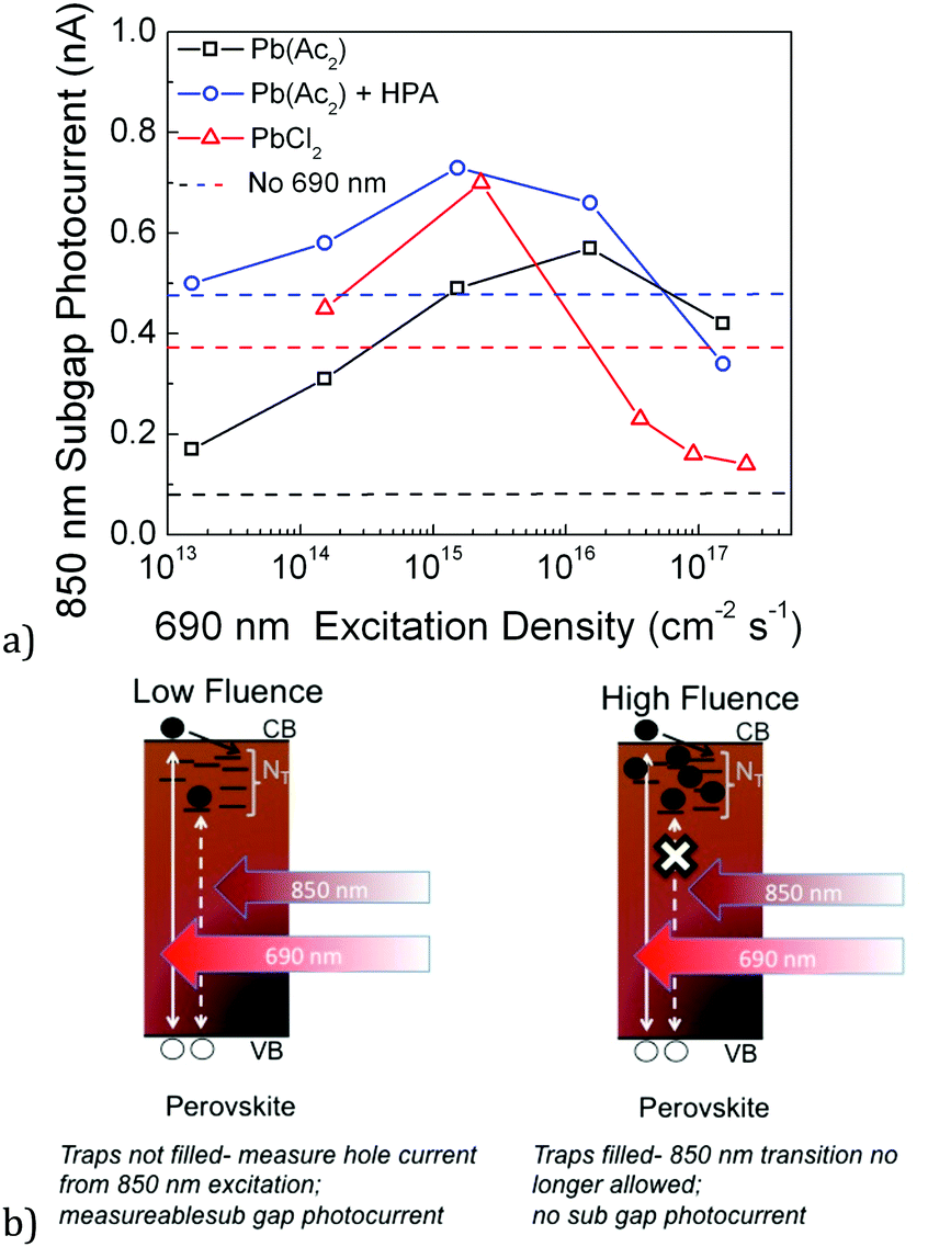 | ||
| Fig. 4 (a) The sub gap photocurrent contribution is monitored as a function of above gap light excitation fluence for devices coated with PMMA. The perovskite films are derived from the Pb(Ac)2 route (with and without HPA treatment) and PbCl2 routes. The sub gap contribution is distinguished by modulating the 850 laser nm and using a lock-in amplifier to detect only this signal. The dashed lines represent the sub gap photocurrent contribution in the absence of any above gap photoexcitation bias. The solid lines are simply to guide the eye, while the data points are denoted by symbols. (b) The schematic depicts the sub gap current generation mechanisms at low and high fluences. | ||
The results indicate that of the three perovskite routes, the PbCl2 route may be the most favorable in terms of achieving a material with low trap densities. However, it has been notoriously difficult to obtain films with 100% coverage of the substrate,42 resulting in pinholes and losses in open circuit voltages. This has led to the use of the Pb(Ac)2 derived perovskite, which forms into extremely smooth and continuous films. However, this appears now to come at the price of a slightly increased trap density. This points to traps being localized predominantly on the surface of crystals, since this route attains smaller grain sizes.40,41 The HPA treatment still allows for the formation of smooth and continuous films, but clearly seems to decrease the trap density and result in a material in which most of the traps are filled, consistent with a slight increase in grain size (though not to the extent of the PbCl2 films).
The most significant behavior observed here is that the different samples exhibit very different points at which their sub gap contribution is strongly diminished, consistent with varying trapping and trapped electron–hole recombination rates. We confirm this again by plotting the transient photocurrent of Pb(Ac)2-derived perovskite films with and without HPA in Fig. S7 (ESI†), where we find that the HPA treatment slows the trapped electron–hole recombination rate as well as the trapping rate itself. This is further evidence that the absolute trap density and processing route of the films affect the rate at which trapped electrons can recombine with free holes, and that not all traps behave the same. Of course, this was already expected from the broad distribution of sites shown in Fig. 1b.
Implications to VOC
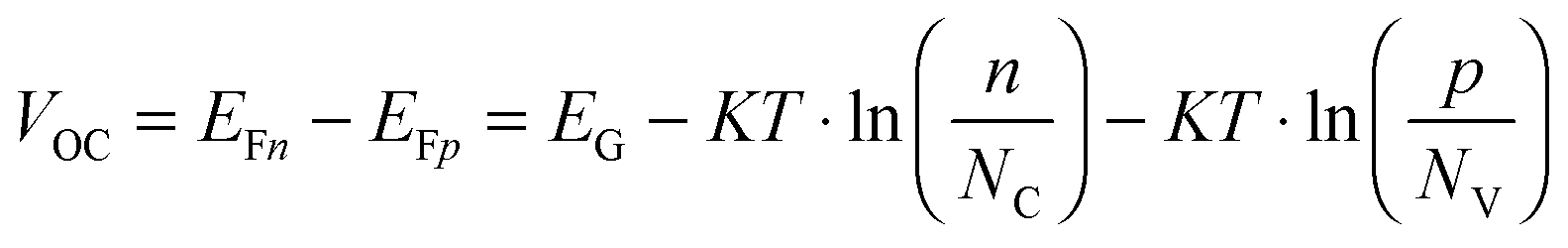
We can take this analysis slightly further, and estimate the obtainable photovoltage due to the effectiveness of Fermi level splitting, bearing in mind what we have learned from the measurements presented here. If the 100 ns (taken as a typical value for many of the perovskite films used throughout different laboratories)6,19,20 electron trapping process resulted in immediate recombination of the trapped electron with a free hole, the effective electron and hole lifetimes would both be 100 ns. Of course, if the trapped electron to free hole recombination rate is extremely slow then it is likely many traps can be filled at solar fluences (as is the case for the PbCl2 derived and HPA treated Pb(Ac)2 derived perovskite films), high hole densities are reached, and only the radiative bimolecular recombination rate becomes increasingly relevant. Using the simple relations shown below,43 it is possible to estimate the maximum obtainable Fermi level splitting and hence a rough approximation of maximum VOC for the three cases: rapid 100 ns trap mediated recombination, a slow trap mediated recombination model vs. complete trap filling at 1 Sun and resultant only bimolecular recombination;| G = R(n,p) | (2) |
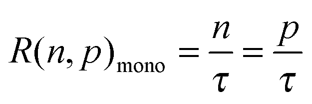 | (3) |
| R(n,p)bimol = n·p·B | (4) |
 | (5) |
| G (cm−3 s−1) | n (cm−3) | p (cm−3) | |EC − EFn| (eV) | |EV − EFp| (eV) | V OC (V) | |
|---|---|---|---|---|---|---|
| 100 ns trap recombination | 2.9 × 10²¹ | 2.9 × 10¹⁴ | 2.9 × 10¹⁴ | 0.23 | 0.23 | 1.14 |
| Traps filled-bimolecular | 2.9 × 10²¹ | 5.7 × 10¹⁵ | 5.7 × 10¹⁵ | 0.15 | 0.16 | 1.30 |
| Long lived holes | 2.9 × 10²¹ | 2.9 × 10¹⁴ | 2.9 × 10¹⁶ | 0.23 | 0.11 | 1.26 |
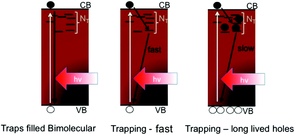 | ||
| Scheme 2 The three different recombination mechanisms considered in Table 1 are schematically illustrated. | ||
This analysis makes it very clear that a rapid trap mediated recombination model with 100 ns trapping and recombination lifetimes would lead to very low electron and hole densities yielding low theoretical VOCs of approximately 1.14 V, which is incompatible with the high experimentally observed values of up to 1.19 V.20 We note that we ignore recombination across the ETL and HTM interfaces with the perovskite, and that the values presented here are very clearly the maximum attainable values assuming ideal contacts. When we consider the results from Fig. 4, which indicate that traps are starting to be filled for the PbCl2 derived material, we must consider the situation where primarily bimolecular recombination affects the carrier dynamics and densities, or at least a situation where most traps are filled and hence the behavior is more akin to the bimolecular case. The photoluminescence quantum yields of perovskite films made in this way have been reported to be 10–30%9,12 at solar fluences, which is in line with a situation where most, but likely not all, traps are filled. In a perovskite film with traps filled, where bimolecular recombination is the dominant mechanism, it becomes possible to obtain high VOCs of approximately 1.3 V, in line with the thermodynamic limit for a 1.6 eV semiconductor and consistent with the highest reported values of 1.19 V in a real device. Considering the situation where traps are far from completely filled, like the case for the Pb(Ac)2 derived perovskite, but including the fact that trapped electrons only recombine with free holes on slow (μs) timescales, we find that it is possible to obtain high VOCs of approximately 1.26 V, still consistent with the high observed voltages even in non-optimized films with significant electron trap densities. In this case, the high hole densities obtained at 1 Sun's worth of excitation mean that radiative recombination will start to compete with the trapping process, i.e. the extremely slow hole recombination will result in increasingly high PLQEs even at low fluences such as at 1 Sun. We make a rough estimation of the relative contribution due to radiative recombination for the fast and slow trap mediated recombination (scenario 1 and 3 in the table) and find that this yields photoluminescence quantum yields of 0.3 and 26%, respectively (see supplemental discussion for details, ESI†). This analysis proves that it is not possible to obtain high quantum yields nor high Fermi level splitting in our perovskite materials if we simply consider 100 ns trapping and recombination time constants. In fact, we now find that the reported quantum yields of 10–30% are only well explained by the fact that trapped carriers are long lived, allowing high enough carrier densities to be reached to facilitate radiative recombination even at 1 Sun. We note that our estimations ignore any non-radiative recombination due to the introduction of the selective contact layers or even other deeper traps through which recombination may be more rapid which we cannot identify here. The charge selective contacts have been shown to limit the ELQE and PLQE of the perovskite devices,44 and thus currently present a severe limitation to the obtainable photo voltages in solar cells. However, our results show that as the contacts continue to improve, we can expect to observe VOCs approaching 1.3 V without any need for further improvement in the optoelectronic quality of the perovskite films themselves.
Conclusions
We have used a combination of transient and steady state photocurrent, absorption, and photoluminescence spectroscopy to study the carrier dynamics in perovskite films over long time scales. Electron trapping is a predominant decay pathway, but the trapped electrons are surprisingly long lived; they only recombine with associated free holes over the course of many microseconds. This allows most of the traps in perovskite films made with typical deposition methods to be filled at solar fluences and hence allow us to rationalize the high VOCs reported for perovskite solar cells, which exceed the limits imposed by a rapid trap mediated recombination model. We furthermore find that due to these fortuitously long lived traps, perovskite films made via existing processing routes exhibit or are close to exhibiting high enough optoelectronic quality to enable solar cells with VOCs approaching 1.3 V provided that non-radiative decays due to contact layers can be mitigated.Experimental
Perovskite fabrication method
Glass substrates were sequentially cleaned with Hellmanex soap, acetone, and isopropanol. Most of the measurements (unless otherwise noted) were performed on perovskite films made via the PbCl2 precursor method. Here, 0.8 M solutions of 3![[thin space (1/6-em)]](https://www.rsc.org/images/entities/char_2009.gif) :1 (by molar concentration) of methylammonium iodide:PbCl2 in DMF were spin coated on oxygen plasma cleaned glass substrates at 2000 rpm for 45 seconds in a nitrogen filled glovebox. The substrates were allowed to dry at room temperature for 30 minutes, then they were annealed at 90 °C for 90 minutes, followed by 120 °C for 20 minutes. The gold electrodes were then thermally evaporated onto the perovskite films through a shadow mask. Then polymethylmethacrylate (PMMA) (20 mg ml−1) or PCBM (20 mg ml−1) or Spiro-OMeTAD (100 mg ml−1) was spin coated on to the perovskite films at 2000 rpm for 45 seconds.
:1 (by molar concentration) of methylammonium iodide:PbCl2 in DMF were spin coated on oxygen plasma cleaned glass substrates at 2000 rpm for 45 seconds in a nitrogen filled glovebox. The substrates were allowed to dry at room temperature for 30 minutes, then they were annealed at 90 °C for 90 minutes, followed by 120 °C for 20 minutes. The gold electrodes were then thermally evaporated onto the perovskite films through a shadow mask. Then polymethylmethacrylate (PMMA) (20 mg ml−1) or PCBM (20 mg ml−1) or Spiro-OMeTAD (100 mg ml−1) was spin coated on to the perovskite films at 2000 rpm for 45 seconds.
For the PbAc2 derived perovskite films, 1 M solutions of 3:1 MAI:PbAc2 with or without 0.0075 M hypophosphorous acid were spin coated at 2000 rpm for 45 seconds. The films were allowed to sit at room temperature for 5 minutes, after which they were annealed at 100 °C for 5 minutes.
Steady state photocurrent measurements
Samples were illuminated using a mechanically chopped laser source (either 650 or 850 as detailed in the main text). A power supply was used to provide a voltage bias across the devices and the current was recorded on a lock-in amplifier in current mode, set to the chopping frequency. The chopping frequency was set to 23 Hz.In the case where a visible light bias was used and only the sub gap contribution was measured, a 690 nm laser was used to continuously illuminate the samples while a mechanically chopped 850 nm laser excitation was used to detect the sub gap contribution. Again, the modulated photocurrent was detected using a lock-in amplifier. In all cases the laser excitation was defocused to cover the entire area between the electrodes. The noise at the output of the lock-in amplifier used here (SR530) is 0.13 pA √Hz−1 and with a specified bandwidth of 0.01 Hz, we have a noise level of 6 fA. This gives more than enough room to measure the pA signals which were the lowest reported in this work.
Excitation density was estimated by assuming that 90% of the above gap excitation was absorbed within the perovskite. The red excitation was used to ensure a fairly uniform absorption profile, and for the sake of simplicity, the total generated carriers were assumed to be uniformly distributed throughout the bulk.
Transient photocurrent spectroscopy
The same samples were excited by 1 ns laser pulses (690 nm, 1 Hz repetition rate), making sure to illuminate the entire area between the electrodes. A power supply was used to bias the sample, while the photocurrent was amplified with a trans-impedance amplifier (gain × 10000) and then measured using an oscilloscope.
To confirm that we are not simply measuring the time for the carrier to be swept out by the electric field, we calculate the sweep-out time using a mobility of 20 cm2 V−1 s−1 as an upper limit. This yields a lower limit sweep out time of 8 ms, far longer than any of the events we have described above.
Transient absorption spectroscopy
Transient absorption (TA) spectroscopy was conducted using an amplified Ti:sapphire laser (100 fs pulses at 800 nm) focused into a sapphire plate to generate a broadband white light probe. The frequency-doubled output of a Q-switched Nd:YVO4 laser acted as a pump (700 ps FWHM pulses at 532 nm), synchronized to the Ti:sapphire laser via a digital delay generator. This setup enables us to perform TA over pump–probe delays from one nanosecond to hundreds of microseconds, covering the timescales of both band-to-band recombination and long lived trap recombination.FTPS
Fourier transform photocurrent spectroscopy was performed using a modified FTIR setup. The excitation was focused onto the perovskite device which was biased by an external power supply. The photocurrent was amplified, recorded, and the interferogram converted to a photocurrent spectrum using a custom designed program.Acknowledgements
The authors acknowledge the funding from the EU Seventh Framework Programme [FP7/2007-203] under grant agreement number 604032 of the MESO project and DESTINY Marie-Curie network under grant agreement number 316494.References
- NREL, Best Research-Cell Efficiencies at http://www.nrel.gov/ncpv/images/efficiency_chart.jpg.
- N. J. Jeon, et al., Compositional engineering of perovskite materials for high-performance solar cells, Nature, 2015, 517, 476–480 CrossRef CAS PubMed.
- A. Miyata, A. Mitioglu, P. Plochocka, O. Portugall, J. T.-W. Wang, S. D. Stranks, H. J. Snaith and R. J. Nicholas, Direct Measurement of the Exciton Binding Energy and Effective 1 Masses for Charge carriers in an Organic-Inorganic Tri-halide Perovskite, Nat. Phys., 2015, 11, 582–587 CrossRef CAS.
- V. D'Innocenzo, et al., Excitons versus free charges in organo-lead tri-halide perovskites, Nat. Commun., 2014, 5, 3586 Search PubMed.
- S. D. Stranks, et al., Electron-Hole Diffusion Lengths Exceeding 1 Micrometer in an Organometal Trihalide Perovskite Absorber, Science, 2013, 342, 341–344 CrossRef CAS PubMed.
- G. Xing, et al., Long-range balanced electron- and hole-transport lengths in organic-inorganic CH3NH3PbI3, Science, 2013, 342, 344–347 CrossRef CAS PubMed.
- C. Wehrenfennig, G. E. Eperon, M. B. Johnston, H. J. Snaith and L. M. Herz, High Charge Carrier Mobilities and Lifetimes in Organolead Trihalide Perovskites, Adv. Mater., 2013, 26, 1584–1589 CrossRef.
- S. De Wolf, et al., Organometallic Halide Perovskites: Sharp Optical Absorption Edge and its Relation to Photovoltaic Performance, J. Phys. Chem. Lett., 2014, 5, 1035–1039 CrossRef CAS PubMed.
- S. D. Stranks, et al., Recombination Kinetics in Organic-Inorganic Perovskites: Excitons, Free Charge, and Subgap States, Phys. Rev. Appl., 2014, 2, 34007 CrossRef.
- Y. Yamada, T. Nakamura, M. Endo, A. Wakamiya and Y. Kanemitsu, Photocarrier Recombination Dynamics in Perovskite CH3NH3PbI3 for Solar Cell Applications, J. Am. Chem. Soc., 2014, 136, 11610–11613 CrossRef CAS PubMed.
- Z.-K. Tan, et al., Bright light-emitting diodes based on organometal halide perovskite, Nat. Nanotechnol., 2014, 1–6, DOI:10.1038/nnano.2014.149.
- F. Deschler, et al., High Photoluminescence Efficiency and Optically Pumped Lasing in Solution-Processed Mixed Halide Perovskite Semiconductors, J. Phys. Chem. Lett., 2014, 1421–1426, DOI:10.1021/jz5005285.
- H. Zhu, et al., Lead halide perovskite nanowire lasers with low lasing thresholds and high quality factors, Nat. Mater., 2015, 636–642 CrossRef CAS PubMed.
- T. Leijtens, et al., Electronic properties of meso-superstructured and planar organometal halide perovskite films: charge trapping, photodoping, and carrier mobility, ACS Nano, 2014, 8, 7147–7155 CrossRef CAS PubMed.
- X. Wu, et al., Trap States in Lead Iodide Perovskites, J. Am. Chem. Soc., 2015, 137, 2089–2096 CrossRef CAS PubMed.
- C. S. Ponseca, et al., Organometal Halide Perovskite Solar Cell Materials Rationalized: Ultrafast Charge Generation, High and Microsecond-Long Balanced Mobilities, and Slow Recombination, J. Am. Chem. Soc., 2014, 136, 5189–5192 CrossRef CAS PubMed.
- W. Shockley and W. T. Read, Statistics of the Recombinations of Holes and Electrons, Phys. Rev., 1952, 87, 835–842 CrossRef CAS.
- E. J. Palomares, J. M. Marin-Beloqui and J. Perez Hernandez, Photo-Induced Charge Recombination Kinetics in MAPbI3-xClx Perovskite-like Solar Cells Using Low Band-Gap Polymers as Hole Conductors, Chem. Commun., 2014, 50, 14566–14569 RSC.
- S. D. Stranks, et al., Electron-hole diffusion lengths exceeding 1 micrometer in an organometal trihalide perovskite absorber, Science, 2013, 342, 341–344 CrossRef CAS PubMed.
- D. Bi, et al., Efficient luminescent solar cells based on tailored mixed-cation perovskites, Sci. Adv., 2016, 2, e1501170 Search PubMed.
- J. P. C. Baena, et al., Highly efficient planar perovskite solar cells through band alignment engineering, Energy Environ. Sci., 2015, 8, 2928–2934 Search PubMed.
- A. Filippetti, P. Delugas and A. Mattoni, Radiative Recombination and Photoconversion of Methylammonium Lead Iodide Perovskite by First Principles: Properties of an Inorganic Semiconductor within a Hybrid Body, J. Phys. Chem. C, 2014, 118, 24843–24853 CAS.
- T. Leijtens, et al., Mapping Electric Field – Induced Switchable Polarization and Structural Degradation in Hybrid Lead Halide Perovskite Thin Films, Adv. Energy Mater., 2015, 5 DOI:10.1002/aenm.201500962.
- C. Trapping, et al., Electronic Properties of Meso-Superstructured and Planar Organometal Halide Perovskite Films, 2014.
- S. Pathak, et al., Atmospheric Influence upon Crystallization and Electronic Disorder and Its Impact on the Photophysical Properties of Organic-Inorganic Perovskite Solar Cells, ACS Nano, 2015, 9, 2311–2320 CrossRef CAS PubMed.
- W.-J. Yin, T. Shi and Y. Yan, Unusual defect physics in CH3NH3PbI3 perovskite solar cell absorber, Appl. Phys. Lett., 2014, 104, 063903 CrossRef.
- M.-H. Du, Density Functional Calculations of Native Defects in CH3NH3PbI3: Effects of Spin–Orbit Coupling and Self-Interaction Error, J. Phys. Chem. Lett., 2015, 6, 1461–1466 CrossRef CAS PubMed.
- I. Borriello, G. Cantele and D. Ninno, Ab initio investigation of hybrid organic-inorganic perovskites based on tin halides, Phys. Rev. B: Condens. Matter Mater. Phys., 2008, 77, 235214 CrossRef.
- A. Rose, Concepts in photoconductivity and allied problems, Interscience publishers, 1963 Search PubMed.
- Y. Shao, Y. Yuan and J. Huang, Correlation of energy disorder and open-circuit voltage in hybrid perovskite solar cells, Nat. Energy, 2016, 1, 15001 CrossRef.
- G. Giorgi, J.-I. Fujisawa, H. Segawa and K. Yamashita, Small Photocarrier Effective Masses Featuring Ambipolar Transport in Methylammonium Lead Iodide Perovskite: A Density Functional Analysis, J. Phys. Chem. Lett., 2013, 4, 4213–4216 CrossRef CAS PubMed.
- A. Filippetti, A. Mattoni, C. Caddeo, M. I. Saba and P. Delugas, Low electron-polar optical phonon scattering as a fundamental aspect of carrier mobility in methylammonium lead halide CH3NH3PbI3 perovskites, Phys. Chem. Chem. Phys., 2016, 18, 15352–15362 RSC.
- D. W. DeQuilettes, et al., Impact of microstructure on local carrier lifetime in perovskite solar cells, Science, 2015, 348, 683–686 CrossRef CAS PubMed.
- B. C. O'Regan, et al., Opto-electronic studies of methylammonium lead iodide perovskite solar cells with mesoporous TiO2; separation of electronic and chemical charge storage, understanding two recombination lifetimes, and the evolution of band offsets during JV hysteresis, J. Am. Chem. Soc., 2015, 137, 5087–5099 CrossRef PubMed.
- A. M. Eppler, I. M. Ballard and J. Nelson, Charge transport in porous nanocrystalline titanium dioxide, Phys. E, 2002, 14, 197–202 CrossRef CAS.
- G. Lakhwani, et al., Probing charge carrier density in a layer of photodoped ZnO nanoparticles by spectroscopic ellipsometry, J. Phys. Chem. C, 2010, 114, 14804–14810 CAS.
- W. Yin, J. Yang, J. Kang, Y. Yan and S.-H. Wei, Halide Perovskite Materials for Solar Cells: A Theoretical Review, J. Mater. Chem. A, 2015, 3, 8926–8942 CAS.
- A. Walsh, D. O. Scanlon, S. Chen, X. G. Gong and S.-H. Wei, Self-Regulation Mechanism for Charged Point Defects in Hybrid Halide Perovskites, Angew. Chem., Int. Ed., 2015, 54, 1791–1794 CrossRef CAS PubMed.
- J. S. Manser and P. V. Kamat, Band filling with free charge carriers in organometal halide perovskites, Nat. Photonics, 2014, 8, 737–743 CrossRef CAS.
- W. Zhang, et al., Ultrasmooth organic–inorganic perovskite thin-film formation and crystallization for efficient planar heterojunction solar cells, Nat. Commun., 2015, 6, 6142 CrossRef CAS PubMed.
- W. Zhang, et al., Enhanced optoelectronic quality of perovskite thin films with hypophosphorous acid for planar heterojunction solar cells, Nat. Commun., 2015, 6, 10030 CrossRef CAS PubMed.
- G. E. Eperon, V. M. Burlakov, P. Docampo, A. Goriely and H. J. Snaith, Morphological control for high performance, solution-processed planar heterojunction perovskite solar cells, Adv. Funct. Mater., 2014, 24, 151–157 CrossRef CAS.
- C. Kittel and D. F. Holcomb, Introduction to solid state physics, Am. J. Phys., 1967, 35, 547–548 CrossRef.
- K. Tvingstedt, et al., Radiative efficiency of lead iodide based perovskite solar cells, Sci. Rep., 2014, 4, 1–7 Search PubMed.
Footnotes |
| † Electronic supplementary information (ESI) available. See DOI: 10.1039/c6ee01729k |
| ‡ Current address: School of Chemistry, Joseph Banks Laboratories, University of Lincoln, Beevor Street, Lincoln LN6 7DL, UK. |
| This journal is © The Royal Society of Chemistry 2016 |