
 Open Access Article
 This Open Access Article is licensed under a Creative Commons Attribution-Non Commercial 3.0 Unported Licence
A scanning probe investigation of the role of surface motifs in the behavior of p-WSe2 photocathodes†
Jesus M.
Velazquez‡
ab,
Jimmy
John‡
 a,
Daniel V.
Esposito
cd,
Adam
Pieterick
be,
Ragip
Pala
be,
Guofeng
Sun
b,
Xinghao
Zhou
be,
Zhuangqun
Huang
f,
Shane
Ardo
g,
Manuel P.
Soriaga
b,
Bruce S.
Brunschwig
bh and
Nathan S.
Lewis
*abhi
a,
Daniel V.
Esposito
cd,
Adam
Pieterick
be,
Ragip
Pala
be,
Guofeng
Sun
b,
Xinghao
Zhou
be,
Zhuangqun
Huang
f,
Shane
Ardo
g,
Manuel P.
Soriaga
b,
Bruce S.
Brunschwig
bh and
Nathan S.
Lewis
*abhi
aDivision of Chemistry and Chemical Engineering, California Institute of Technology, 1200 E. California Blvd., Pasadena, CA 91125, USA
bJoint Center for Artificial Photosynthesis, California Institute of Technology, 1200 E. California Blvd., Pasadena, CA 91125, USA
cDepartment of Chemical Engineering, Columbia University in the City of New York, 500 W. 120th St., New York, NY 10027, USA
dNational Institute of Standards and Technology, Materials Measurement Laboratory, 100 Bureau Drive, Gaithersburg, MD 20899-1070, USA
eDivision of Engineering and Applied Science, California Institute of Technology, 1200 E. California Blvd., Pasadena, CA 91125, USA
fBruker Nano Surfaces, 122 Robin Hill Road, Goleta, CA 93101, USA
gDepartment of Chemistry and Department of Chemical Engineering and Materials Science, University of California at Irvine, Irvine, CA 92697, USA
hMolecular Materials Research Center, Beckman Institute, California Institute of Technology, Pasadena, CA 91125, USA
iKavli Nanoscience Institute, California Institute of Technology, Pasadena, CA 91125, USA. E-mail: nslewis@caltech.edu
First published on 8th October 2015
Abstract
The spatial variation in the photoelectrochemical performance for the reduction of an aqueous one-electron redox couple, Ru(NH3)63+/2+, and for the evolution of H2(g) from 0.5 M H2SO4(aq) at the surface of bare or Pt-decorated p-type WSe2 photocathodes has been investigated in situ using scanning photocurrent microscopy (SPCM). The measurements revealed significant differences in the charge-collection performance (quantified by the values of external quantum yields, Φext) on various macroscopic terraces. Local spectral response measurements indicated a variation in the local electronic structure among the terraces, which was consistent with a non-uniform spatial distribution of sub-band-gap states within the crystals. The photoconversion efficiencies of Pt-decorated p-WSe2 photocathodes were greater for the evolution of H2(g) from 0.5 M H2SO4 than for the reduction of Ru(NH3)63+/2+, and terraces that exhibited relatively low values of Φext for the reduction of Ru(NH3)63+/2+ could in some cases yield values of Φext for the evolution of H2(g) comparable to the values of Φext yielded by the highest-performing terraces. Although the spatial resolution of the techniques used in this work frequently did not result in observation of the effect of edge sites on photocurrent efficiency, some edge effects were observed in the measurements; however the observed edge effects differed among edges, and did not appear to determine the performance of the electrodes.
Broader contextInvestigations of bare and platinized p-WSe2 single crystals implicate microscopic terraces as the major sites of performance losses; warranting a revisit of the traditionally accepted paradigm of edges as the sole source of deleterious electron–hole recombination. We utilized scanning photocurrent microscopy, under relevant electrochemical environments, to spatially differentiate performance at the microscale. Further studies by a suite of ex situ scanning probe techniques were conducted to probe the relationship between surface topography and performance. |
1. Introduction
Semiconductors made from layered transition-metal dichalcogenides (TMDCs) of molybdenum and tungsten (MX2; where M = Mo, W and X = S, Se) have band-gap energies (Eg) in the ranges of 1.0 eV to 1.5 eV (indirect) and 1.4 eV to 2.3 eV (direct), have large absorption coefficients (≈105 cm−1 and ≈106 cm−1 for photon energies above Eg,indirect and Eg,direct, respectively), and can be doped n-type or p-type.1,2 These properties make TMDCs attractive for use in solar-driven water-splitting devices that contain two semiconductors arranged in series with respect to the incident illumination, with the semiconductors having complementary band gaps for optimum energy conversion.3 Integration of Pt/Ru catalysts for the hydrogen-evolution reaction (HER) onto p-WSe2 photocathodes has yielded hydrogen-evolving photocathodes with ideal regenerative cell efficiencies4 of greater than 7% under mildly acidic conditions (pH = 4.2).5 Single crystal n-type layered TMDCs, specifically n-WSe2 and n-MoSe2, provide robust photoanodes for halide oxidation in aqueous environments, and have been used in regenerative cells to obtain high photovoltaic system efficiencies4 (greater than 17%)6 as well as stability for over 10 months of continuous operation.7,8Chemically inert, defect-free terraces of TMDCs may afford interfaces with properties advantageous for device performance. For example, deposition of metals onto MoS2 single crystals has been shown to form Schottky junctions with no evidence for Fermi-level pinning or deleterious interfacial states.9 The TMDCs have also been shown to facilitate fabrication of heterojunctions by van der Waals (vdW) epitaxy.10,11 However, integration of TMDCs into prototypes of photoelectrosynthetic devices has been hindered by the inability to produce photoactive forms of these materials in a scalable fashion.1 The synthesis of large (≈1.0 cm2), high-performance, defect-free single crystals using a chemical-vapor-transport (CVT) technique has required precise control over temperature gradients at high temperatures (greater than 900 °C) for long periods of time (1 week to 2 weeks).12,13 Thin films of the TMDCs can be synthesized by a variety of scalable methods such as wet-chemical synthesis,14 electrodeposition,15 short-term chemical-vapor transport,16 chemical-vapor deposition17,18 and, more recently, by solution-based self-assembly methods.19 However, compared to single crystals, thin films have many electronic and crystallographic defects, and consequently exhibit low photoactivity.19–21
The surfaces of TMDCs consist of multiple terraces separated by step edges. Previous work suggests that edge sites are deleterious to the photoconversion efficiency because the under-coordinated atoms on the edges are reactive toward surface corrosion processes22 and additionally act as sites for charge-carrier recombination.23,24 Hence, relatively higher photoconversion efficiencies have been attributed to surface motifs composed predominantly of larger terraces and a lower density of step edges, while relatively lower photoconversion efficiencies have been attributed to surface motifs composed predominantly of smaller terraces and a greater density of step edges.
We describe herein the use of a suite of in situ spatially resolved electrochemical techniques to explore the relationship between the surface morphology and the photoelectrochemical performance of single-crystal p-WSe2 photocathodes. Using these methods, the photoelectrochemical performance of bare p-WSe2 photocathodes have been evaluated in contact with an aqueous solution that contains an electrochemically reversible, one-electron-transfer redox couple. Additionally, the performance of p-WSe2 photocathodes coated with an electrodeposited Pt HER catalyst has been evaluated in contact with 0.5 mol L−1 H2SO4(aq). Therefore, by elucidating the structure–property–performance relationships of these WSe2 photoelectrodes, this work provides valuable information for guiding the design of more efficient TMDC photoelectrodes.
2. Experimental
2.1. Synthesis of p-WSe2 single crystals
p-WSe2 single crystals were synthesized by a chemical vapor-transport method.5 Briefly, 1.57 g of polycrystalline WSe2 powder (prepared in-house), 0.28 g of WO2Cl2 (Sigma Aldrich, St. Louis, MO), excess elemental Se bulk powder (0.154 g, Sigma Aldrich), and 0.003 g of Nb (Sigma Aldrich) were loaded at the sealed end of a quartz ampule, which was then vacuum-sealed. The ampule was then heated under a temperature gradient (≈2 °C cm−1) with the charge zone at 1000 °C and the growth zone at ≈950 °C for ≈7 days.2.2. Preparation of photoelectrodes and photoelectrochemical cell
To expose fresh surfaces, freestanding p-WSe2 single crystals were mechanically exfoliated with Scotch tape. Single crystals were then mounted onto a Si substrate that had been coated with In metal solder. Single crystals of p-WSe2 were then placed on top of the In layer while the In was molten, to facilitate electrical contact between the crystal and the In layer. A Cu wire was then soldered onto the front corner of the In/Si substrate, and two-part epoxy (Hysol 9460) was utilized to seal the back and edges of the electrode, leaving exposed only the front surface of the p-WSe2 single crystal. Photoelectrodes were cured overnight and were then mounted in a custom-made, low-profile, Teflon-based photoelectrochemical cell that fit onto the stage of a Raman microscope. The sample was securely affixed to the base of the Teflon cell by application of 3M-brand electroplaters tape on top of the sample. An appropriately sized window was cut beforehand in the electroplaters tape so that only the front face of the single-crystal photoelectrode contacted the solution during the electrochemical measurements. The geometric electrode area exposed to the solution was ≈3 mm2. A glass slide was placed over the cell and the 3M electroplaters tape was then used to seal the glass to the cell, to make the entire assembly leak-proof. Fig. S1 (see ESI†) shows the steps in the assembly and mounting of the p-WSe2 sample in the custom cell.2.3. Electrochemistry
To prepare solutions for the electrochemical experiments, [Ru(NH3)6]Cl3 (98%, Sigma Aldrich), KH2PO4 (crystal, AR ACS, Macron Chemicals), H2SO4 (99.999% trace metal basis, Sigma Aldrich), and H2PtCl6·6H2O (ACS reagent, ≥37.50% Pt basis) were obtained and used without further purification. The de-ionized water had a resistivity >18.2 MΩ cm as generated from a Barnstead Nanopure system (Thermo Scientific, Asheville, NC, USA) and was used for making solutions. A BioLogic SP-200 (Biologic, Grenoble, France) or a CHI 760 D (CH Instruments, Austin, TX, USA) potentiostat was used for electrochemical measurements. A high surface area Pt wire (99.99% trace metal basis, Sigma-Aldrich) was used as a counter electrode and a saturated Ag/AgCl electrode (0.197 V versus NHE, either obtained from CH Instruments or custom-made) housed in a micro-agar-gel salt bridge was used as the reference electrode.2.4. Deposition of Pt nanoparticles onto p-WSe2 electrodes
As described previously, photoelectrodeposition was used to deposit Pt particles onto p-WSe2 photoelectrodes.5 Briefly, bare p-WSe2 photoelectrodes were loaded into a standard 3-electrode electrochemical cell and the electrodes were placed in contact with a plating solution that consisted of 1 mmol L−1 H2PtCl6 in 0.1 mol L−1 HCl(aq). The photoelectrodes were biased at −0.1 V versus a saturated calomel electrode (SCE) while the samples were exposed for 1 minute to 3 minutes to chopped (≈1 Hz) illumination from an ELH-type W-halogen lamp at ≈1 Sun of light intensity.2.5. Scanning photocurrent microscopy (SPCM)
Experiments were performed using a Horiba Jobin Yvon LabRAM Raman microscope system equipped with an Olympus BX41 microscope, and a uEyE CCD camera. A Ventus VIS 532 nm laser (Laser Quantum) was used as the excitation source. Before every SPCM experiment, the laser power at the surface of an unmounted sample in air (outside the photoelectrochemical cell) was measured using a Thorlabs Gmbh optical meter. The laser beam was focused on the photodiode of the optical meter to obtain the incident laser power. The values for laser power reported herein were measured using the photodiode, and were not corrected for attenuation of the beam due to adventitious absorption by the electrochemical cell components (the cover glass slide and the electrolyte layer). The incident laser power was typically ≈4 μW and the laser beam was typically ≈4 μm in diameter.The assembled photoelectrochemical cell was mounted securely on the translation stage under the objective of the microscope. The laser beam was then focused on the surface of the photoelectrode in the area of interest. Three types of local photocurrent measurements were generally performed: (1) linear sweep voltammetry (LSV), in which the laser beam was stationary and the potential of the photoelectrode was varied while the photocurrent was measured; (2) line scans, in which the laser beam was scanned in a straight line over a feature of interest while a constant potential was applied to the photoelectrode and while the photocurrent was measured, thereby providing the local photocurrent response as a function of the beam position; (3) 2-D external quantum yield (Φext) maps, in which the laser beam was rastered across a rectangular region of interest on the photoelectrode surface while a constant potential was applied to the photoelectrode and while the photocurrent was measured, thereby providing photocurrent data that were processed to generate a 2-D color map of the photocurrent response over the scanned region. The photocurrent values were converted to external quantum yield (Φext) values for clarity of representation and cross-comparison of maps as given by eqn (1):
 | (1) |
2.6. Local spectral response
Spatially resolved photocurrent measurements were obtained using a Fianium supercontinuum white-light source coupled to a Spectra Physics monochromator. The photocurrent signal was measured with an SRS830 lock-in amplifier connected to a Biologic SP-200 potentiostat. The surface of the sample was illuminated with a Gaussian beam using a 5× Mitutoyo objective that provided a ≈4 μm diameter spot.2.7. Microscopy of as-synthesized p-WSe2 and Pt decorated p-WSe2
A scanning electron microscope (SEM – Nova NanoSEM 450) operated at an accelerating voltage range of 5 kV to 15 kV was used to determine the surface topography, such as edges and terraces. Optical micrographs were acquired using a long-working-distance 10× objective (Olympus America Inc.).Atomic-force microscopy (AFM, Bruker Dimension Icon with ScanAsyst) was used to characterize the morphology of the electrode surfaces. The ScanAsyst mode is based on the Peak-Force Tapping mechanism, and performs a fast force-curve capture at every pixel in the image, with the peak force of each curve used as the imaging feedback signal. The ScanAsyst-air probes (Bruker) had a nominal tip radius of 2 nm (maximum tip radius of 12 nm, silicon tip; silicon nitride cantilever, nominal spring constant: 0.4 N m−1, ranges from 0.2 N m−1 to 0.8 N m−1; frequency: 50 Hz to 90 kHz). For conductive AFM, the Peak-Force Tunneling AFM mode was used. This mode is also based on the Peak-Force Tapping principle and allows mapping of the surface topography in addition to simultaneous measurement of tunneling current signals when the tip is in contact with the substrate surface. A PFTUNA conductive AFM probe (Bruker, nominal tip radius 25 nm, maximum tip radius of 35 nm) was used to complete the electric circuit for the conductivity measurement, with an electrical potential of 2 V applied between the AFM tip and the sample substrate.
Ultra-high vacuum scanning-tunneling microscopy (UHV-STM, Omicron) was used to identify the presence of intrinsic defects. An oxide-free surface was obtained before loading the sample into the UHV chamber by exfoliating a fresh surface of p-WSe2 single crystals with Scotch tape. To remove adsorbed water from the surface, the sample was degassed overnight at ≈550 °C in UHV. The STM tip (TT-ECM10, Bruker) was heated by an electron beam to remove the oxide layer. UHV-STM measurements were performed at room temperature, with a base pressure of 10−7 Pa and a scanning rate of 3 lines per second at a tip bias of ≈4 V.
3. Results
3.1. Morphology of p-WSe2 surfaces
Fig. 1 shows SEM and UHV-STM images of the surface of p-WSe2 crystals. The p-WSe2 surface exhibited features on a variety of length scales. While edges and terraces resulting from the layered structure of the material were the dominant apparent features on length scales on the order of 10 μm to 100 μm (Fig. 1a and b), at length scales of a few nanometers point defects were also apparent on exfoliated crystals (Fig. 1c and d). UHV-STM data revealed the presence of nanometer-scale defects that appeared dark in contrast and were distributed randomly on terraces (Fig. 1c and d). These defects are consistent in appearance with prior STM studies of chalcogen vacancies on TMDC surfaces.25–28 AFM images showed that the large (greater than 10 μm) terraces observed by SEM were composed of smaller terraces that were a few microns in width (see Fig. S2, ESI†). | ||
| Fig. 1 (a) Scanning-electron microscope (SEM) image showing edges and terraces of p-WSe2. (b) SEM image of a region on a p-WSe2 crystal exhibiting a high density of edge sites. (c) Scanning-tunneling microscope (STM) image showing apparent black spots on the surface of a p-WSe2 terrace. (d) High-resolution STM image showing isolated Se vacancies that appear dark in contrast. | ||
3.2. Photocurrent response at edge sites
The effects of the edges on photocurrent were examined by collecting line scans across the edges of bare p-WSe2 electrodes in contact with 10 mmol L−1 Ru(NH3)63+/0.5 mol L−1 KH2PO4(aq) (Fig. 2 and Fig. S3, ESI†). The photocurrent versus distance responses across the edges could be generally classified into two categories: (i) a sigmoidal (or S-shaped) response, in which a step change in the photocurrent was observed as the laser beam crossed the edge (see Fig. 2a and b) and (ii) a peaked response, in which a peak was observed in the photocurrent versus distance curve as the laser beam traversed the edge (see Fig. 2c and d). Sigmoidal responses were observed far more commonly than peaked responses. The prevalence of the sigmoidal response showed that two terraces that shared an edge generally did not have the same photoactivity and hence differences in photocurrent between the adjacent terraces dominated the photocurrent change at the edge. Peaked responses indicated that the photocurrents on the neighboring terraces were not too dissimilar. The edges did not, however, exhibit consistent behavior, and both negative (Fig. 2c) and positive (Fig. 2d) peaks were observed. Moreover, in some cases, the photoactivity differences between adjacent terraces and the contribution from the edge were both significant, and a convolution in the photocurrent response was observed between the sigmoidal and the peaked behavior (see Fig. S3, ESI†). | ||
| Fig. 2 Typical photocurrent line scans obtained from bare p-WSe2 electrodes in contact with 10 mmol L−1 Ru(NH3)63+/0.5 mol L−1 KH2PO4(aq) and illuminated by a 532 nm laser. Applied potential: −0.05 V vs. Ag/AgCl. (a) Sigmoidal photocurrent response across two neighboring terraces. Incident laser power: 3.86 μW. Scan speed: 1.2 μm s−1. (b) Photocurrent response across a set of adjacent terraces showing lower photocurrent from the smaller terraces. Incident laser power: 12.61 μW. Scan speed: 0.4 μm s−1. (c) and (d) Line scans across a pair of neighboring terraces showing a decrease and an increase in photocurrent at the macroscopic edges respectively. Incident laser power: 3.86 μW and 12.48 μW for (c) and (d) respectively. Scan speeds: 1.7 μm s−1 and 0.4 μm s−1 for (c) and (d) respectively. Scale bar: 10 μm. | ||
3.3. Mapping the photoactivity of terraces
 | ||
| Fig. 3 Scanning photocurrent microscopy (SPCM) measurements at a p-WSe2 electrode in contact with 10 mmol L−1 Ru(NH3)63+/0.5 mol L−1 KH2PO4(aq) before and after platinization, as well as of the same electrode in contact with 0.5 mol L−1 H2SO4(aq) after platinization. (a) Optical image of the area of interest. (b) Photocurrent measured as a function of beam position during a line scan as indicated by the white arrow in (a). Scan speed: 2.5 μm s−1. (c) Linear sweep voltammograms (LSVs) obtained at locations A and B as indicated in (a) before and after platinization. Scan rate: 20 mV s−1 (d) 2-D map of external quantum yield (Φext) for the area demarcated by the dotted rectangle in (a). Scan speed: 11 μm s−1. Applied potential: −0.05 V vs. Ag/AgCl for (b) and (d). Incident laser power: 4.13 μW. (e) Linear sweep voltammograms (LSVs) obtained at locations A and B in (a) after platinization and in contact with 0.5 M H2SO4(aq). Scan rate: 20 mV s−1. (f) 2-D Φext map of the area denoted by the dotted rectangle in (a) after platinization and in contact with 0.5 mol L−1 H2SO4(aq). Applied potential: −0.13 V vs. Ag/AgCl. Scan speed: 14 μm s−1. Incident laser power: 4.2 μW. For all SPCM measurements, beam spot size: ≈10 μm and beam wavelength: 532 nm. | ||
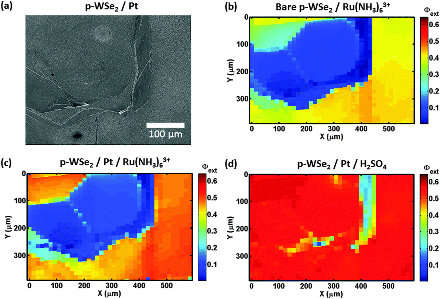
Fig. 4b shows a Φext map for a second bare p-WSe2 photoelectrode in contact with 10 mmol L−1 Ru(NH3)63+/0.5 mol L−1 KH2PO4(aq). The photoconversion from the terrace in the middle of the image (blue) had a low Φext that was less than 0.10 relative to the behavior of the surrounding terraces (Φext > 0.30). Fig. S4b (ESI†) likewise shows a Φext map for a third bare p-WSe2 photocathode under similar conditions, and depicts terraces that exhibited low Φext values adjacent to terraces having higher Φext values. The differences in the photoactivities of the terraces were not related to variations in light absorption/scattering across the sample surface, as no correlation was observed between the reflectance and the Φext of the samples (Fig. S4c, ESI†).
 | ||
| Fig. 4 Comparison of maps of external quantum yield (Φext) for an area of a p-WSe2 electrode before and after platinization and in contact with 10 mmol L−1 Ru(NH3)63+/0.5 mol L−1 KH2PO4(aq) or 0.5 mol L−1 H2SO4(aq). (a) Scanning electron microscope (SEM) image of the area of the platinized photoelectrode where scanning photocurrent microscopy (SPCM) measurements were performed. The granularity seen on the crystal surface is from the deposited Pt nanoparticles. 2-D Φext maps of the area corresponding to the SEM image: (b) bare p-WSe2 and (c) Pt/p-WSe2 in contact with 10 mmol L−1 Ru(NH3)63+/0.5 mol L−1 KH2PO4(aq). (d) Pt/p-WSe2 in contact with 0.5 mol L−1 H2SO4(aq). Applied potential: −0.05 V vs. sat. Ag/AgCl for (b) and (c), −0.13 V vs. sat. Ag/AgCl for (d). Scan speed: ca. 17 μm s−1. Beam spot size: ≈10 μm. Beam wavelength: 532 nm. | ||
Fig. 4c shows the Φext map for the second photoelectrode after platinization and in contact with 10 mmol L−1 Ru(NH3)63+/0.5 mol L−1 KH2PO4(aq). On the areas surrounding the low-Φext terrace, Pt slightly improved the photoconversion relative to the bare electrode (Φext ≈ 0.50 at Pt/p-WSe2 compared to ≈0.40 at bare p-WSe2). Fig. S6 (ESI†) shows a map of the change in Φext for Pt/p-WSe2 relative to bare p-WSe2.
Fig. 4d shows the performance of another platinized p-WSe2 photoelectrode for HER in 0.5 mol L−1 H2SO4(aq). For this sample, the photoconversion at the terraces correlated more closely with the distribution of the Pt nanoparticles (Fig. 4a) than with the intrinsic quality of the terraces. The terrace that exhibited low Φext (<0.15) in contact with Ru(NH3)63+, with or without Pt, Fig. 4b and c showed high photoconversion efficiencies (Φext ≈ 0.55) for HER that were essentially equal to those observed in the adjacent areas of the sample (Fig. 4d). The areas of the map that had very low Φext (<0.25, vertical strip at x = ≈400 μm, see Fig. 4d), corresponded to areas where less Pt was visible (see Fig. 4a and Fig. S8a, ESI†).
 | ||
| Fig. 5 (a) Optical image of an area of a bare p-WSe2 electrode where local spectral measurements were carried out. The locations are denoted by the dots with the numbers identifying them. (b) and (c) Local spectral response curves obtained at various locations shown in (a) on the surface of the bare p-WSe2 electrode in contact with 10 mmol L−1 Ru(NH3)63+/0.5 mol L−1 KH2PO4(aq). The number identifying the location – with the value of external quantum yield (Φext) at 533 nm (Φext,533) in brackets – is shown beside each curve in (b) and (c). For the sake of presentation, the local spectral responses are categorized based on the value of Φext,533: (b) locations that had Φext,533 > 0.15 and (c) locations that had Φext,533 < 0.15. Applied potential: −0.05 V vs. sat. Ag/AgCl. The area highlighted in grey represents the wavelength region below the direct bandgap of WSe2 (Eg,direct = 1.57 eV or 790 nm). The dotted vertical line indicates the wavelength around which the shoulder feature is observed in the spectral response. The local Φext values are separately normalized to their values at λ = 533 nm to facilitate comparison of the respective sub-band-gap responses. The un-normalized Φext curves are included in Fig. S9 (ESI†). | ||
4. Discussion
Step edges on TMDC's are generally considered to be the primary source of photoconversion-efficiency losses via the recombination of photogenerated charge carriers at edge sites.23,24,29,30 Some evidence suggests that passivated edges act as enhanced carrier-collection sites aided by rapid charge-carrier transport parallel to the layers.31–36 In this work, neither losses nor improvements in the photoconversion efficiency were universally observed at edge sites. However, a remarkable variation was observed in the photoelectrochemical behavior between different terraces and this spatial variability could be a significant source of the photoconversion-efficiency losses in these materials. Within a group of terraces, the smaller terraces generally exhibited lower Φext than neighboring larger terraces, but the dimensions of the smaller terraces were still large (on the order of 50 μm to 100s of μm) relative to the maximum minority-carrier diffusion length reported for WSe2 (≈4 μm).31 Although Φext varied amongst terraces, Φext values were generally uniform within the boundaries of each terrace, and Φext did not decrease near the boundaries of the terraces. These observations suggest that defects that lead to poor performance of a terrace are uniformly distributed within the terrace rather than localized at edge sites.4.1. Role of the macroscale edges and their effect on line scans
The photocurrent behavior near the step edges can be understood based on a model modified from one originally developed by Lewerenz et al. for layered TMDCs (Fig. 6).23,29,30 Due to the layered structure of TMDCs, a high degree of anisotropy is present in the transport and in the electrical properties of these materials between the directions parallel and normal to the layers.12 The transport of carriers parallel to the layers is more rapid than the transport normal to the layers, because the latter requires inter-layer hopping and thus relies on an extrinsic conduction mechanism that is slower than the intrinsic intra-layer transport within the plane of the layers.30 The minority-carrier diffusion length in p-WSe2 parallel to the layers, Ln,∥, has been estimated at ≈4 μm,31 in contrast to that normal to the layers, with Ln,⊥ ≈ 1.6 μm.23 In Fig. 6, the space-charge (depletion) region established relative to the terraces is labeled W⊥ while that relative to the step edges is labeled W∥. Charges generated in these space-charge regions are assumed to efficiently move to either the surface of the terrace or to the edge. The net result, due to faster transport along layers, is that electrons that are photogenerated within a distance of W∥ + Ln,∥ from the edge are deflected toward the edge. | ||
| Fig. 6 Schematic depicting the fate of photo-generated carriers near a step edge for p-MX2 (based on prior work23,29,30). W∥ and W⊥ are the depletion widths parallel and normal to the layers respectively. δp (≈W∥, W⊥) is the optical absorption depth, Ln,∥ (≫W∥, W⊥) is the minority-carrier diffusion length parallel to the layers, and d is the step height. | ||
In the model advanced by Lewerenz et al.23,29,30 the edge sites were hypothesized to act exclusively as recombination centers, and thus the photocurrent was expected to decrease at each edge. To account for our observation of both negative and positive peaks in the photocurrent response at the edges (see Fig. 2c and d), the model has been modified to allow edge sites to additionally act as sites for facile interfacial charge transfer (“hot” sites).
The depletion width (W) can be estimated by the equation:
 | (2) |
The height of the step edge, d, is variable from site to site. The step heights observed optically for this work varied from 80 nm to 500 nm. When step edges are small relative to δp (≈100 nm), the carrier-capture cross-section of those step edges will be small compared to the carrier-capture cross section of the adjacent terraces, because carriers are photogenerated at depths greater than the edge height and thus are created within layers to which the edge does not extend. Hence, any photocurrent response at these small step edges would be undiscernible in our measurements. Only larger edges (d ≫ δp) would be expected to show an appreciable effect in the photocurrent measurements. Step edges with heights much less than the beam-penetration depth are inconsequential to the photoconversion efficiency of the photoelectrode suggesting that particularly high-performing electrodes could be constructed from single-layer or thin films of TMDCs. However, an efficient photoelectrode must possess a thickness sufficient to absorb the incident light (≈10 nm for absorption by the direct band gap of WSe2),1,2 whereas single-layer TMDCs possesses thicknesses of only about 6.5 Å.
The size of the scanning laser-beam spot (≈5 μm) used in this work is comparable to the reported value of Ln (1 μm to 4 μm), and is significantly larger than the depletion width (≈100 nm). Hence, the spot size limits the ability of the experimental methods employed in this work to measure changes in photocurrent arising from the presence of edges. Scanning laser measurements using laser spot sizes of ≈15 μm to 25 μm have been performed previously for n-WSe2 samples to topographically investigate efficiency losses in photoanodes while oxidizing iodide.24,33 Such measurements have shown a decrease in photocurrent in edge-rich regions. Because the laser spot sizes used in those studies were 3 to 5 times larger than the spot size used herein, the methods employed herein ought to provide an opportunity to observe edge effects for more favorable cases, for example if W∥ at some edges was comparable to the beam spot size (possibly due to deviation of the local dopant density from the bulk value).
The framework described above can be used to understand the two kinds of photocurrent responses – the sigmoidal response and the peaked response – that were observed at the macro-scale edges in the line-scan measurements. At least three main factors determine the photoresponse at an edge: (i) the difference in the intrinsic photoactivities of the terraces sharing an edge, quantified by the difference in their photocurrents far away from the edge (|Δiterraceph|); (ii) the ratio of the height of the edge to the penetration depth i.e. d/δp; and (iii) the nature of the edge; whether it acts as a recombination site or as a “hot” (interfacial charge transfer) site.
In this framework, purely sigmoidal responses are observed at edges that are “short” (i.e. d/δp ≪ 1) or, in other words, that have small minority-carrier capture cross-sections and that have large differences in the photoactivities of the terraces straddling the edge (i.e. |Δiterraceph| ≫ 0). The limiting case for observing a peaked response is therefore for the edge to be “tall” (i.e. d/δp ≫ 1) and for the photoactivities of the terraces to be similar (|Δiterraceph| ≈ 0), with the nature of the edge (whether it acts as a recombination site or a “hot” site) determining the sign of the peak. However, in general, the photoresponse at an edge will be a superposition of the sigmoidal response from the terraces and the peaked response from the edge.
Experimentally, the measurements show each of the three cases. Predominantly sigmoidal responses were observed for the line scans shown in Fig. 2a and b. The photoresponse in Fig. 2d is the closest to representing the effect of just the edge. Enhanced collection of charge carriers at edge sites may reflect passivation of such sites. For example, formation of WO3 at the step edges may replace deleterious surface states with states outside of the band gap of WSe2. This has been demonstrated previously using electron-beam-induced-current microscopy at the interface between WSe2/WO3 at edge sites created by (photo)electrochemical etching the WSe2.31,33–35 Although in our work edge sites were not created using (photo)electrochemical etching, a pristine, unetched, freshly cleaved crystal exposed to air may possess passivated, oxidized edges that do not act as recombination centers. If photogenerated charge carriers were deflected toward passivated edges sites, the probability of collecting such carriers would be increased near the edge site relative to the terrace site, and would result in an increase in photocurrent near the edge relative to the terrace. Finally, the combined effect of the terraces and the edges, with variable photoresponse at the edge, is shown in Fig. S3 (ESI†). The finding that significantly more sigmoidal-type responses were observed than peaked responses is consistent with expectations for the situation in which having macroscopic terraces of unequal photoactivity is the norm rather than the exception.
4.2. Variations in the photoactivity of the terraces
A varying photoresponse was observed between terraces on the p-WSe2 photocathodes. When investigated using scanning probe methods, microscopic terraces that appeared optically smooth exhibited texturing in the form of nanoscale terraces and dislocations (Fig. S2, ESI†). No correlation was apparent between the microscale edge density (as measured by AFM) on optically visible terraces and the photoconversion efficiency for reduction of Ru(NH3)63+ (Fig. 7). In addition to variations in the size of the terraces and the related variation in the average distance that photogenerated charge carriers can travel laterally before reaching an edge, the variation in performance among terraces may also be related to a non-uniform distribution of surface and bulk defect states. | ||
| Fig. 7 (a) External quantum yield (Φext) versus micro-scale edge density for a bare p-WSe2 in contact with 10 mmol L−1 Ru(NH3)63+/0.5 mol L−1 KH2PO4(aq). Applied potential: −0.05 V vs. sat. Ag/AgCl. Beam wavelength: 533 nm. (b) Representative AFM image showing edges separated by micron-sized terraces within a macroscale terrace bounded by visible edges. In (a), a series of such AFM topographic images obtained at different locations on the surface of the bare p-WSe2 photoelectrode were used to plot the measured micro-scale edge densities versus the values of Φext at the corresponding locations on the electrode. | ||
The UHV-STM data (Fig. 1c and d) revealed the presence of defects likely due to Se vacancies randomly distributed on a terrace. Bicelli et al.38 observed variations between different areas of n-MoSe2 electrodes for photo-iodide production, and attributed the differences to the presence of terraces having non-stoichiometric chalcogen-to-metal ratios. Previous studies on the use of MoS2 as a hydrodesulfurization (HDS) catalyst have noted that the Mo![[thin space (1/6-em)]](https://www.rsc.org/images/entities/char_2009.gif) :S ratio correlates with the HDS catalytic activity and bulk conductivity character (n or p-type).39,40 A suite of combined STM, SPM and spatially resolved XPS studies on bulk MoS2 samples has recently been used to reveal significant spatial variation in the Mo:S ratio at the surface of MoS2.28 The study showed that both p- and n-doped regions co-exist on the surface of MoS2, depending on whether an excess or deficiency, respectively, of S was present locally. Furthermore, S vacancies have been shown to modify the local electronic structure and to introduce surface states within the band gap of MoS2.25,26
:S ratio correlates with the HDS catalytic activity and bulk conductivity character (n or p-type).39,40 A suite of combined STM, SPM and spatially resolved XPS studies on bulk MoS2 samples has recently been used to reveal significant spatial variation in the Mo:S ratio at the surface of MoS2.28 The study showed that both p- and n-doped regions co-exist on the surface of MoS2, depending on whether an excess or deficiency, respectively, of S was present locally. Furthermore, S vacancies have been shown to modify the local electronic structure and to introduce surface states within the band gap of MoS2.25,26
As shown in Fig. 5, the local electronic structure varied from terrace to terrace. Low-photoactivity terraces exhibited spectral features at sub-bandgap wavelengths that were not present on higher activity terraces, indicative of the presence of defect states.24 Defect states typically act as charge-carrier recombination centers, and therefore can be expected to be detrimental to photoactivity. However, when defect states are positioned at energies between the conduction-band minimum and E° for the contacting redox couple, in this case Ru(NH3)63+/2+, radiation at energies too low to excite carriers into the conduction band can still excite carriers into the defect state. Although recombination may still dominate the charge-carrier dynamics in such a case, a fraction of the photoexcited carriers can still successfully be transferred to the electroactive species in solution.
4.3. Comparison of photoreduction of Ru(NH3)63+(aq) with photo-HER at terraces
Ru(NH3)63+/2+ is an electrochemically reversible one-electron redox couple, whereas reduction of 2H+ to H2(g) requires the transfer of two electrons. The latter reaction requires a substantial kinetic overpotential, η > 700 mV, to obtain a current density of −10 mA cm−2 (see Fig. S10, ESI†) on bare single-crystalline p-WSe2 electrodes. By contrast, Pt is a low-overpotential catalyst for the HER (η ≈ 30 mV at −10 mA cm−2),41 and thus significantly reduces the overpotential required to catalyze the HER compared to that required for p-WSe2 photocathodes. However, Pt has a much smaller effect on the photoelectrochemical performance in the single-electron transfer Ru(NH3)63+ reduction, for which the fast kinetics proceed easily on the WSe2 surface itself. Some improvement was observed in the photoconversion efficiency for platinized p-WSe2 for the HER compared to the same sample for Ru(NH3)63+ reduction, with the most significant effects (≈0.10 to 0.20 improvement in Φext) observed for terraces that performed poorly for Ru(NH3)63+ photoreduction in the absence of Pt (Fig. 4c and Fig. S5d, ESI†). The relative increases in photoconversion efficiency due to platinization of p-WSe2 electrodes (ΔΦext = ΦPtext − ΦBareext, where ΦBareext and ΦPtext are external quantum yields before and after platinization) were significantly greater for photo-HER than for photoreduction of Ru(NH3)63+, by ≈0.15 to 0.40 (i.e. ΔΦHERext − ΔΦRu-hexext ≈ 0.15–0.40, where ΔΦHERext and ΔΦRu-hexext are the relative increases in external quantum yields for photo-HER and photoreduction of Ru(NH3)63+ respectively due to platinization).The standard reduction potential, E°, for 2H+/H2(g) at pH = 0.3 is −0.22 V versus Ag/AgCl (sat. KCl), while E°(Ru(NH3)63+/2+) = −0.130 V versus Ag/AgCl (sat. KCl). Thus, a larger built-in voltage should be obtained from p-WSe2 electrodes in contact with 2H+/H2(g) than for p-WSe2/Ru(NH3)63+/2+(aq) junctions, and this additional built-in voltage may result in the observed higher photoconversion efficiency for the HER than for Ru(NH3)63+ reduction.
The differences in the observed photoelectrochemical behavior at different terraces on platinized samples correlated with differences in the amount of platinum on the surface. This result is expected because, for photo-HER, only charge carriers generated within the minority-carrier diffusion length of a Pt particle can contribute to the reaction. The Pt catalyst was deposited by reductive photoelectrodeposition; thus, the photoactivity of the terraces could be convoluted with the distribution of the Pt. Such a situation would result in greater improvements in efficiency at terraces that, when bare, were relatively high-performing, as observed for the case of platinized samples in contact with Ru(NH3)63+/2+.
5. Conclusion
The SPCM investigation of p-WSe2 photocathodes revealed considerable variation in the photoconversion efficiency of terraces of the layered structures. The variation in the photoconversion efficiency among terraces may be due to a non-uniform distribution of surface and bulk defect states among terraces, particularly chalcogen vacancies. Local spectral response measurements indicated a variation in the local electronic structure between terraces, and specifically, spectral features at energies below the band gap were observed for terraces with relatively poor photoconversion efficiencies, indicative of the presence of surface states.Some effects of edge sites were apparent as peaks in the photocurrent line scans; however, different edges exhibited different types of behavior. The photoconversion efficiencies of p-WSe2 photocathodes decorated with Pt were greater for the HER than for reduction of a one-electron-transfer redox couple with fast kinetics, Ru(NH3)63+/2+. Additionally, terraces with low photoconversion efficiency for Ru(NH3)63+ reduction could in some cases yield high Φext for the HER. The spatial distribution of the Pt catalyst was non-uniform owing to the deposition method employed, and appeared to have greater influence over the varied photoconversion efficiency for the HER at different terraces than the quality of the terraces themselves.
Based on the results of our studies, a prospective roadmap can be formulated for application of layered TMDCs as light absorbers in solar fuel devices. For optimization of single-crystal TMDCs, identifying and rectifying the cause of low-performing terraces to ensure uniformly high photoactivity across the photoelectrode surface should constitute the highest priority. Secondly, the effect of the macroscopically visible edges is not critical in determining the photoelectrode performance. In fact, Tenne and coworkers have demonstrated better performance for iodide oxidation on photo-etched samples of n-WSe2 that had higher densities of edges compared to freshly cleaved samples.31–36 In addition, passivation of edge sites does not necessarily overcome poor photovoltaic properties of terraces, and as evidenced from the results shown herein, the behavior of photoactive terraces will dominate the overall positive or negative performance. Therefore, thin films that contain a high density of edge sites could potentially be used in photoactive devices if the corresponding terraces are synthesized with minimal content of in-gap states and bulk defects and if the films are synthesized with sufficient thickness to absorb the incident visible light. Strategies developed to control the surface motifs present on TMDC single crystals should be readily translatable and attractive for improvement of the photoactivity of polycrystalline thin-film forms of TMDCs.
Acknowledgements
This material is based upon work performed by the Joint Center for Artificial Photosynthesis, a DOE Energy Innovation Hub, supported through the Office of Science of the U.S. Department of Energy under Award No. DE-SC0004993. Additional support for this work was provided by BP. JMV acknowledges support through an NRC Ford Foundation Postdoctoral Fellowship and the U.S. Department of Energy under Award No. DE-SC0004993. JJ thanks the Camille and Henry Dreyfus Foundation for financial support through its postdoctoral fellowship program in environmental chemistry and the U.S. Department of Energy, Office of Basic Energy Sciences under Award No. DE-FG02-03ER15483. DVE acknowledges support from the NIST NRC Fellowship program. JMV, JJ, and DVE also acknowledge the NIST Center for Nanoscale Science and Technology for use of its facilities for some SPCM measurements. SA acknowledges support from a United States Department of Energy, Office of Energy Efficiency and Renewable Energy (EERE) Postdoctoral Research Award under the EERE Fuel Cell Technologies Program. Certain commercial equipment, instruments, and materials are identified in this paper to foster understanding. Such identification does not imply recommendation or endorsement by the National Institute of Standards and Technology, nor does it imply that the materials or equipment identified are the best available for the purpose.References
- A. Aruchamy, Photoelectrochemistry and photovoltaics of layered semiconductors, Kluwer Academic, Dordrecht, Boston, 1992 Search PubMed.
- J. A. Wilson and A. D. Yoffe, Adv. Phys., 1969, 18, 193–335 CrossRef CAS.
- M. G. Walter, E. L. Warren, J. R. McKone, S. W. Boettcher, Q. Mi, E. A. Santori and N. S. Lewis, Chem. Rev., 2010, 110, 6446–6473 CrossRef CAS PubMed.
- R. H. Coridan, A. C. Nielander, S. A. Francis, M. T. McDowell, V. Dix, S. M. Chatman and N. Lewis, Energy Environ. Sci., 2015, 8, 2886–2901 CAS.
- J. R. McKone, A. P. Pieterick, H. B. Gray and N. S. Lewis, J. Am. Chem. Soc., 2013, 135, 223–231 CrossRef CAS PubMed.
- G. Prasad and O. N. Srivastava, J. Phys. D: Appl. Phys., 1988, 21, 1028–1030 CrossRef CAS.
- G. Kline, K. Kam, D. Canfield and B. A. Parkinson, Sol. Energy Mater., 1981, 4, 301–308 CrossRef CAS.
- H. Tributsch, Sol. Energy Mater., 1979, 1, 257–269 CrossRef CAS.
- J. Lince, D. Carré and P. Fleischauer, Phys. Rev. B: Condens. Matter Mater. Phys., 1987, 36, 1647–1656 CrossRef CAS.
- K. Ueno, T. Shimada, K. Saiki and A. Koma, Appl. Phys. Lett., 1990, 56, 327 CrossRef CAS.
- X. Zhang, F. Meng, J. R. Christianson, C. Arroyo-Torres, M. A. Lukowski, D. Liang, J. R. Schmidt and S. Jin, Nano Lett., 2014, 14, 3047–3054 CrossRef CAS PubMed.
- E. Bucher, in Photoelectrochemistry and photovoltaics of layered semiconductors, ed. A. Aruchamy, Kluwer Academic, Dordrecht, Boston, 1992, pp. 1–81 Search PubMed.
- M. Lenz and R. Gruehn, Chem. Rev., 1997, 97, 2967–2994 CrossRef CAS PubMed.
- F. H. Saadi, A. I. Carim, J. M. Velazquez, J. H. Baricuatro, C. C. L. McCrory, M. P. Soriaga and N. S. Lewis, ACS Catal., 2014, 2866–2873 CrossRef CAS.
- S. Chandra and S. N. Sahu, Phys. Status Solidi A, 1985, 89, 321–331 CrossRef CAS.
- J. M. Velazquez, F. H. Saadi, A. P. Pieterick, J. M. Spurgeon, M. P. Soriaga, B. S. Brunschwig and N. S. Lewis, J. Electroanal. Chem., 2014, 716, 45–48 CrossRef CAS.
- D. Kong, H. Wang, J. J. Cha, M. Pasta, K. J. Koski, J. Yao and Y. Cui, Nano Lett., 2013, 13, 1341–1347 CrossRef CAS PubMed.
- Y. Yu, C. Li, Y. Liu, L. Su, Y. Zhang and L. Cao, Sci. Rep., 2013, 3, 1866 Search PubMed.
- X. Yu, M. S. Prévot, N. Guijarro and K. Sivula, Nat. Commun., 2015, 6, 7596 CrossRef PubMed.
- H. D. Abruna and A. J. Bard, J. Electrochem. Soc., 1982, 673 CrossRef CAS.
- D. S. Ginley, R. M. Biefield, B. A. Parkinson and K. K. Kan, J. Electrochem. Soc., 1982, 145 CrossRef CAS.
- Z. Chen, A. J. Forman and T. F. Jaramillo, J. Phys. Chem. C, 2013, 117, 9713–9722 CAS.
- H. J. Lewerenz, S. D. Ferris, C. J. Doherty and H. J. Leamy, J. Electrochem. Soc., 1982, 129, 418 CrossRef CAS.
- B. A. Parkinson, T. E. Furtak, D. Canfield, K.-K. Kam and G. Kline, Faraday Discuss. Chem. Soc., 1980, 70, 233 RSC.
- S. Kc, R. C. Longo and R. M. Wallace, Nanotechnology, 2014, 25, 375703 CrossRef PubMed.
- N. Kodama, T. Hasegawa, T. Tsuruoka, C. Joachim and M. Aono, Jpn. J. Appl. Phys., 2012, 51, 5–9 CrossRef.
- M. Makarova, Y. Okawa and M. Aono, J. Phys. Chem. C, 2012, 116, 22411–22416 CAS.
- S. McDonnell, R. Addou, C. Buie, R. M. Wallace and C. L. Hinkle, ACS Nano, 2014, 8, 2880–2888 CrossRef CAS PubMed.
- H. J. Lewerenz, J. Electrochem. Soc., 1984, 131, 100 CrossRef CAS.
- H. J. Lewerenz, A. Heller and F. J. DiSalvo, J. Am. Chem. Soc., 1980, 102, 1877–1880 CrossRef CAS.
- A. Jakubowicz, D. Mahalu, M. Wolf, A. Wold and R. Tenne, Phys. Rev. B: Condens. Matter Mater. Phys., 1989, 40, 2992–3000 CrossRef CAS.
- D. Mahalu, A. Jakubowicz, A. Wold and R. Tenne, Phys. Rev. B: Condens. Matter Mater. Phys., 1988, 38, 1533–1536 CrossRef CAS.
- D. Mahalu, L. Margulis, A. Wold and R. Tenne, Phys. Rev. B: Condens. Matter Mater. Phys., 1992, 45, 1943–1946 CrossRef CAS.
- D. Mahalu, M. Peisach, W. Jaegermann, A. Wold and R. Tenne, J. Phys. Chem., 1990, 94, 8012–8013 CrossRef CAS.
- R. Tenne, K. Eherman, D. Mahalu, M. Peisach, W. Kautek, A. Wold, R. Matson and D. H. Waldeck, Ber. Bunsen-Ges., 1993, 97, 702–708 CrossRef CAS.
- R. Tenne and A. Wold, Appl. Phys. Lett., 1985, 47, 707 CrossRef CAS.
- R. F. Frindt, J. Phys. Chem. Solids, 1963, 24, 1107–1108 CrossRef CAS.
- L. P. Bicelli and G. Razzini, Surf. Technol., 1983, 20, 383–392 CrossRef CAS.
- A. Aoshima and H. Wise, J. Catal., 1974, 34, 145–151 CrossRef CAS.
- P. R. Wentrcek and H. Wise, J. Catal., 1976, 45, 349–355 CrossRef CAS.
- W. Sheng, H. A. Gasteiger and Y. Shao-Horn, J. Electrochem. Soc., 2010, 157, B1529 CrossRef CAS.
Footnotes |
| † Electronic supplementary information (ESI) available. See DOI: 10.1039/c5ee02530c |
| ‡ These authors contributed equally to this work. |
| This journal is © The Royal Society of Chemistry 2016 |