
Planar heterojunction organometal halide perovskite solar cells: roles of interfacial layers
Hobeom
Kim†
,
Kyung-Geun
Lim†
 and
Tae-Woo
Lee
*
and
Tae-Woo
Lee
*
Department of Materials Science and Engineering, Pohang University of Science and Technology (POSTECH), Pohang 790-784, Republic of Korea. E-mail: twlee@postech.ac.kr; taewlees@gmail.com
First published on 13th October 2015
Abstract
Organometal halide perovskites are promising photo-absorption materials in solar cells due to their high extinction coefficient, broad light absorption range and excellent semiconducting properties. The highest power conversion efficiency (PCE) of perovskite solar cells (PrSCs) is now 20.1%. However, a high-temperature processed mesoscopic metal oxide (e.g., TiO2) must be removed to realize flexible PrSCs on plastic substrates using low temperature processes. Although the planar heterojunction (PHJ) structure can be considered as the most appropriate structure for flexible PrSCs, they have shown lower PCEs than those with a mesoscopic metal oxide layer. Therefore, development of interfacial layers is essential for achieving highly efficient PHJ PrSCs, and necessary in fabrication of flexible PrSCs. This review article gives an overview of progress in PHJ PrSCs and the roles of interfacial layers in the device, and suggests a practical strategy to fabricate highly efficient and flexible PHJ PrSCs. We conclude with our technical suggestion and outlook for further research direction.
 Hobeom Kim | Hobeom Kim is currently a PhD candidate in the Department of Materials Science and Engineering at Pohang University of Science and Technology (POSTECH), Korea. He received his BS in the School of Advanced Materials Science and Engineering from Sungkyunkwan University (SKKU), Korea in 2011. His current research activity is focused on perovskite and flexible optoelectronics. |
 Kyung-Geun Lim | Kyung-Geun Lim received his BS in the Department of the Nanoscience and the Nanotechnology from Pusan National University, Korea in 2009, MS and PhD in the Department of Materials Science and Engineering from Pohang University of Science and Technology (POSTECH), Korea in 2011 and 2015 respectively, under supervision of Prof Tae-Woo Lee. He has been performing research on the improvement of device efficiency and lifetime of organic solar cells (OSCs) and perovskite solar cells (PrSCs). His current research interests include understanding various mechanisms of charge extraction layers in OSCs and PrSCs. |
 Tae-Woo Lee | Tae-Woo Lee is an associate professor in the Department of the Materials Science and Engineering at Pohang University of Science and Technology (POSTECH), Korea. He received his PhD in Chemical Engineering from KAIST, Korea in 2002. Then, he joined Bell Laboratories, USA as a postdoctoral researcher. He worked in Samsung Advanced Institute of Technology as a member of research staff (2003–2008). He received a prestigious Korea Young Scientist Award from the President of Korea in 2008 and The Scientist of the Month Award from the ministry of science, ICT and future planning in 2013. His research focuses on printed electronics and optoelectronics based on organic, inorganic, and organic–inorganic hybrid perovskite materials for flexible electronics, displays, solid-state lightings, and solar energy conversion devices. |
1. Introduction
Organometal metal halide perovskites are promising materials for various optoelectronic and photonic devices including solar cells,1–4 light-emitting diodes,5–7 and photodiodes.8–10 Furthermore, low threshold lasing has been reported from these materials.11–13 Active research based on organic–inorganic hybrid perovskites has focused on perovskite solar cells (PrSCs) because of the recent rapid achievements in increasing their power conversion efficiency (PCE): the first liquid-junction PrSCs were reported in 200914 and PCEs of solid-state PrSCs reached 20.1% in 2015.4This rapid increase in PCE has been achieved mainly by improving the device architecture and fabrication techniques. In addition to high PCE, PrSCs have two great advantages. (1) Organic–inorganic hybrid perovskites have a high absorption coefficient, so a thin (<500 nm) film of perovskite light absorber is sufficient as a photo-active layer in PrSCs. Therefore, the devices can be thin and light. (2) With these features, flexible, large-area PrSCs can be fabricated at low cost. Because of these advantages and high PCE, PrSCs have the potential to replace conventional Si solar cells, and to provide portable, mobile, and wearable power sources.
PrSCs have inherited the architecture of dye-sensitized solar cells (DSSCs),15–17 most of which include a mesoscopic metal oxide layer (e.g., TiO2), so the structure of early-stage PrSCs was similar to those of DSSCs,14,18 and many studies still present mesoscopic PrSCs with very high PCEs. However, this type of PrSC cannot be developed as a flexible device because the formation of the mesoporous structure requires high temperature T > 450 °C, which damages most flexible plastic substrates. Also, the high-T processes for development of mesoscopic PrSCs make it difficult to complete the tandem structure which is a promising configuration for increasing PCE of solar cells, but need low-T processable interconnecting layers between bottom and upper cells to avoid destruction of layers underneath it.
Instead, the use of planar heterojunction (PHJ) PrSCs that include low-T processable interlayers without the mesoscopic structure can provide a method to fabricate flexible PrSCs and tandem PrSCs. Furthermore, nonuse of the mesoscopic structure simplifies the structure of PrSCs and reduces the cost and time for fabrication. Theoretical and experimental research on PHJ PrSCs has led to PCE > 19%.19 Many studies on PHJ PrSCs to date have focused on engineering of the perovskite film as a photo-active layer to make it favourable for solar cells,20–46 but studies on interlayer engineering of PrSCs are relatively lacking. PHJ PrSCs with high open circuit voltage Voc, high short circuit current Jsc, and high fill factor FF can be achieved by using appropriate interfacial layers between the electrodes and perovskite light absorber. Basically, to maximize the built-in potential of the device and to facilitate charge transfer from perovskite to interfacial layers, the PHJ PrSCs should use a hole extraction layer (HEL) and an electron extraction layer (EEL) with well-matching ionization energy (IE) and electron affinity (EA), respectively, to those of perovskites.47–49 Also, the use of interfacial layers with high electrical conductivity is favourable to make efficient charge transport and extraction to each electrode.
The defect chemistry of perovskites is another topic of study. Traps in the perovskite film and at the interface between perovskite and interfacial layers have a strong influence on the photophysical and photoelectrical properties of devices and thereby on device performance. High density of the trap states results in non-radiative recombination which is an undesirable physical process in PrSCs that leads to hysteresis behaviour, depending on photocurrent measurement conditions.50–54 Due to these reasons, to improve the performance of PHJ PrSCs, the interfacial layers between the electrodes and perovskite absorber must be engineered appropriately.
In this review, we focus on the development of PHJ PrSCs which have a strong potential to be applied to flexible devices, and especially focus on the work on interfacial layer engineering. Sections 2 and 3 provide basic explanations of structural and physical properties of perovskites and on progress in PrSCs, particularly those of the PHJ type. Section 4 reviews the functions of interfacial layer in PHJ PrSCs. Section 5 reviews research on flexible PHJ PrSCs. Section 6 presents conclusions.
2. Principles of organic–inorganic perovskite materials
Perovskites are crystal structures that have originated from the calcium titanium oxide mineral (CaTiO3). Generally, perovskites have an ABX3 formula, where cation A is located at the corner positions (0,0,0), cation B is at the centre (1/2,1/2,1/2) and monovalent anion X is at the centre of the six planes (1/2,1/2,0) assuming them as the idealized cubic unit cell (Fig. 1). The most widely-used component materials of perovskites for PrSCs are organic molecule cations based on amine at A sites (e.g., CnH2n+1NH3+, HC(NH2)2+), metal cations (e.g., Pb2+, Sn2+, Cu2+) at B sites, and halide anions (Cl−, Br−, I−) at X sites. Various kinds of organic–inorganic hybrid perovskites are based on the configuration that Mitzi et al. formulated by incorporating an organic modulation layer between metal halide sheets.55 The formation of perovskite structures can be estimated from the tolerance factor56and octahedral factor

| μ = RB/RX, |
 | ||
| Fig. 1 (a) Crystal structure of an organic–inorganic perovskite. (b) The generated species, free carriers or excitons after photo-excitation of the perovskite. | ||
Some perovskites (e.g., MAPbI3, MAPbIxCl3−x and FAPbI3 [MA: methylammonium CH3NH3, FA: formamidinium HC(NH2)2]) have broad absorption spectra with a suitable band gap ∼1.5–1.6 eV, and therefore are used as light absorbers in PrSCs. In addition to absorption spectra, perovskites that are suitable as light harvesters in PrSCs should have an appropriate dielectric constant ε, exciton binding energy Eb, Bohr radius, and diffusion length of charge carriers. These factors have a strong relationship with photophysical and photoelectrical properties and solar cell device performance. The photo-generated electron–hole pairs in these organic–inorganic perovskites can exist as free charge carriers or excitons with Eb, and the excitons can be classified as Frenkel-type or Wannier-type depending on the perovskite Eb. Many researchers have reported that the Eb of perovskite materials (29–50 meV for MAPbI358–61 and 35–98 meV for MAPbCl3−xIx62,63) comparable to thermal energy (∼25 meV) at room temperature facilitates exciton dissociation. Recently, there has been a report that MAPbI3 has an Eb of 2 meV which is very lower compared to inorganic semiconductors (e.g., Si, 15.0 meV; GaAs, 4.2 meV; CdTe, 10.5 meV).64 Although which species are generated under illumination and what is the make-up of the species in perovskite materials are still under debate, free carriers easily dissociated from excitons contribute to ambipolar charge transport in the materials.65,66 Based on these excellent capabilities of light absorption and photophysical/photoelectrical properties, perovskites are considered as promising materials for solar cell devices.
3. Progress in perovskite solar cells
3.1. Mesoscopic vs. Planar
Miyasaka et al. (2009) developed the first PrSCs; the devices had a perovskite photosensitizer but otherwise had a structural configuration nearly identical to conventional DSSCs.14 The structure of devices was TiCl4 treated fluorine-doped tin oxide (FTO) (anode)/mesoporous TiO2/perovskite sensitizer/Pt-coated FTO (cathode); the gap between the electrodes was filled with liquid electrolyte. With this structure, the PCEs of devices using MAPbBr3 and MAPbI3 were 3.13 and 3.81%, respectively. Subsequent research by Park et al. (2011) used the initial liquid-junction device configuration and achieved an improved PCE = 6.5%, but the liquid electrolyte dissolved the perovskite crystal, so stability of the device could not be guaranteed.18 This problem was solved by using a solid-state hole conductor, spiro-OMeTAD, on top of the perovskite layer instead of using the liquid electrolyte;1 the resulting device showed long-term stability for over 500 h and PCE > 9% (Fig. 2a–e). Grätzel et al. (2013) introduced a sequential deposition method in which PbI2 was first deposited on a mesoporous metal oxide and transformed into a perovskite by exposing methylammonium iodide (MAI).3 Using this method, the devices had greatly increased reproducibility and PCE ≈ 15% (Fig. 2f and g). Seok et al. (2014) achieved a PCE = 16.2% by depositing a uniform and dense perovskite layer by using a mixed solvent of γ-butyrolactone and dimethylsulphoxide (DMSO), and then drop-casting toluene.67 Very recently, Seok et al. (2015) achieved a record PCE > 20% by exploiting the intramolecular exchange process between formamidinium iodide (FAI) and DMSO molecules intercalated in PbI2 (Fig. 2h and i).4 This remarkably rapid progress in development of PrSCs and several advantages such as thinness, light weight, and inexpensive processability have made PrSCs appropriate for various solar cell applications.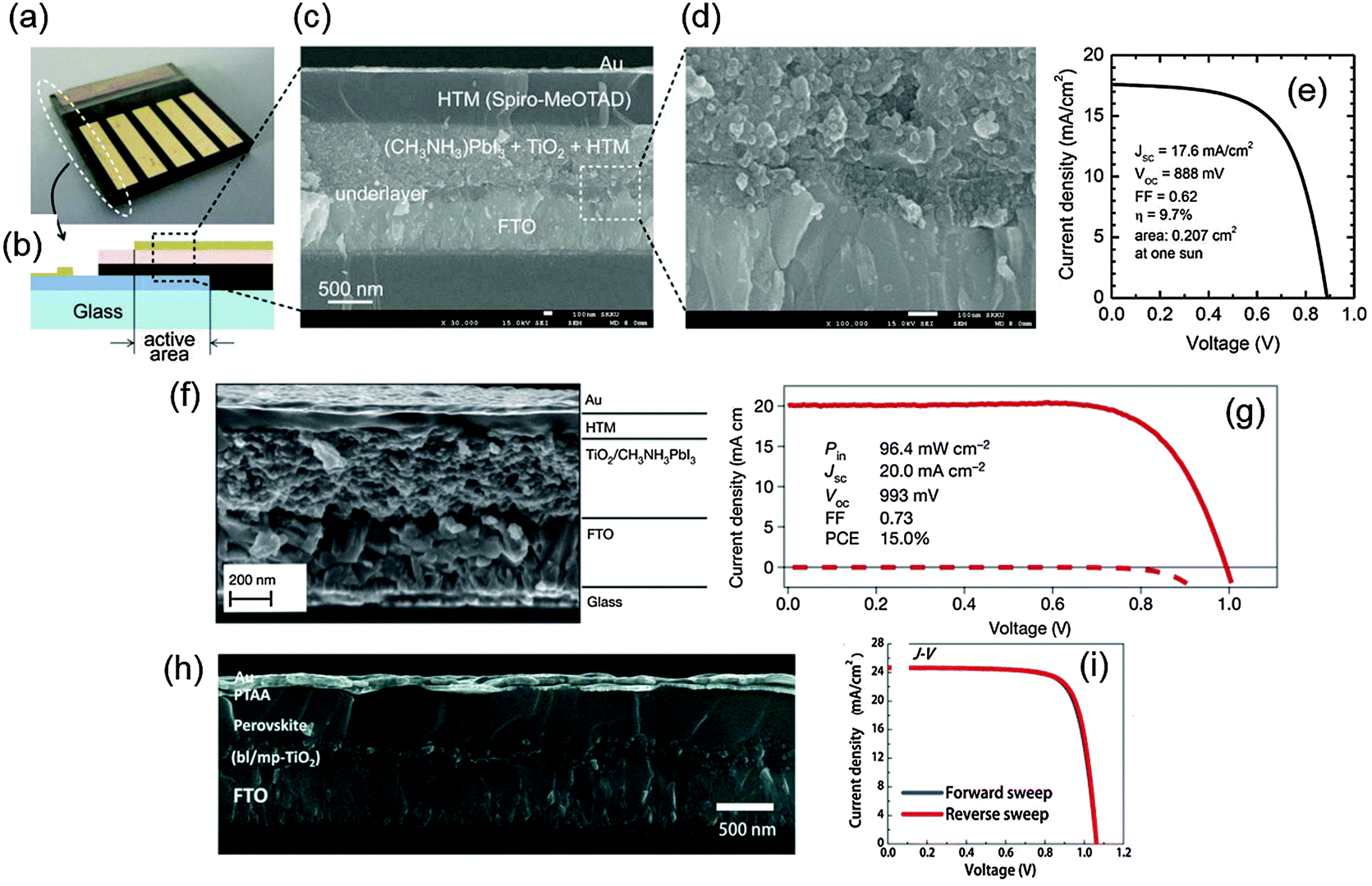 | ||
| Fig. 2 Device configurations and J–V characteristics of mesoscopic PrSCs. (a) A real device of the first solid-state mesoscopic perovskite solar cells. (b) A schematic image of the device cross-section. (c) The SEM image of the device cross-section. (d) The magnified cross-sectional SEM image of the FTO/underlayer/active layer region. (e) J–V characteristics of the device at one sun condition. Reproduced from ref. 1 with permission from Nature Publishing Group. (f) The cross-sectional SEM image of another mesoscopic perovskite solar cell. (g) J–V characteristics of the device under simulated AM1.5G solar irradiation (solid line) and in the dark (dashed line) (reproduced from ref. 3 with permission from Nature Publishing Group). (h) The cross-sectional FESEM image of the device with PCE over 20%. (i) J–V characteristics of the device measured in reverse and forward directions under standard AM 1.5G illumination. Reproduced from ref. 4 with permission from Science (AAAS). | ||
Many electronic devices including PrSCs are being developed toward a flexible configuration for future electronics. However, mesoscopic PrSCs cannot easily be made flexible because generally the mesoscopic structure should be sintered at T > 450 °C to function as an EEL in a device,1–4 but most available flexible substrates (e.g., PET, PEN) have a glass transition temperature that is lower than the sintering temperature, so the polymer substrates deform under high sintering temperature. Therefore, to establish flexible PrSCs, a new device structure that can be fabricated at low T is required.
PHJ PrSCs that do not use the mesoscopic structure are practical options for flexible PrSCs owing to their low-T processability. PHJ PrSCs are divided into two groups according to the layer stacking sequence: i.e., the conventional n–i–p structure in which the EEL is deposited on the bottom cathode first, the HEL is underneath the top anode layer, and the perovskite is sandwiched between EEL and HEL; and the p–i–n structure, which is the inverse of the n–i–p type.
The n–i–p configuration of PHJ devices was introduced in 2013 as a modification of meso-superstructured (MSSC) PrSCs that incorporated a mesoporous insulating scaffold of Al2O3 on a compact TiO2 layer.68 The device had a PCE = 4.9% without a mesostructure which is the PHJ type; the authors described that the MAPbI3−xClx perovskite absorber can fulfill both light absorption and efficient charge transport with minimal recombination in the film. Based on these results, they questioned whether a mesostructure is essential in PrSCs. Although the device included a high-T (>500 °C) processed compact TiO2 layer, many researchers then sought to develop n–i–p type PHJ PrSCs that could be fabricated using low-T processing.19,69–82
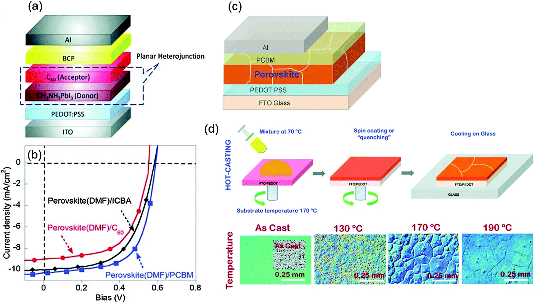
The p–i–n type PHJ PrSC was first developed by Guo et al. in 2013.83 The researchers noticed that the concept of donor/acceptor could be applicable to the device and introduced the structure after referring to a previous work by Etgar et al., who reported that the MAPbI3 perovskite acts as both the light absorber and hole conductor.84 The first p–i–n PHJ PrSC employed poly(3,4-ethylenedioxythiophene) polystyrene sulfonate (PEDOT:PSS) as a p-type layer for hole extraction, and fullerene-based molecules as the acceptor (n-type) that were deposited on the perovskite (donor) layer. In addition to PEDOT:PSS, various kinds of efficient p-type layers such as NiOx,85 CuSCN,86 graphene oxide (GO)87 and reduced graphene oxide (rGO)88 for p–i–n type PHJ PrSCs have been reported. Most p–i–n type devices can be fabricated at T < 150 °C, so this configuration is regarded as the most suitable for flexible devices.
3.2. Progress in low-temperature processed PHJ PrSCs
In this section, we present some examples and progress of solution processed n–i–p and p–i–n type PHJ PrSCs, and vacuum processed PHJ devices.Grätzel et al. improved the suitability of a TiO2 layer on FTO for electron extraction by immersing the substrate in TiCl4 solution at T = 70 °C;78 the resultant TiO2 was a rutile nanoparticle that could form an intimate nanocrystalline junction with a perovskite layer (Fig. 3a). A device with the FTO/TiO2/MAPbI3/Spiro-OMeTAD/Au structure achieved a PCE = 13.7% (Fig. 3b). Boyen et al. used the TiO2 layer as an ETL based on titanium isopropoxide processed at a low T = 135 °C.70 The device had the ITO/TiO2/MAPbI3−xClx/P3HT/Ag structure and a PCE = 13.6%; the authors stated that the chemical composition and conditions of thermal treatment on the TiO2 film have critical effects on the device performance. Yang et al. achieved PCE up to 19.3% (average 16.6%) which is so far the highest value in an n–i–p type PHJ PrSC (Fig. 3c and d).19 The authors introduced an enhanced reconstruction process for the perovskite film by annealing the as-deposited film in humidity-controlled air. For efficient electron transport, they chose poly-(ethyleneimine ethoxylated) (PEIE) processed at 100 °C and Yttrium-doped TiO2 processed at 150 °C. From transient photovoltage and photocurrent measurements, they found that an extended electron carrier lifetime and reduced trap densities in the perovskite film and faster photocurrent decay of the device using modified TiO2 contributed superior device performance. In addition to the TiO2-based EEL, researchers have developed other low-T processable EELs such as ZnO nanoparticles, CdSe nanocrystals, SnO2, WOx, and phenyl-C61-butyric acid methyl ester (PC61BM).67,69,71–73,75,77
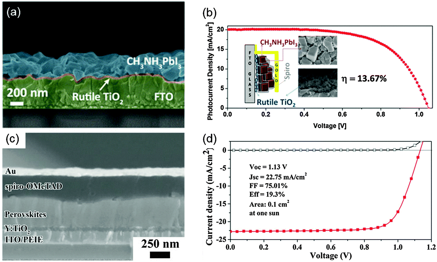 | ||
| Fig. 3 (a) Cross-sectional SEM image of a perovskite film deposited on the nanocrystalline TiO2 film. (b) J–V curves of the n–i–p PHJ PrSC device that used rutile TiO2. The inset shows a schematic image of the device and SEM images of perovskite and rutile TiO2 layers. Reproduced from ref. 78 with permission from the American Chemical Society. (c) The cross-sectional SEM image of the n–i–p PHJ PrSC device. (d) J–V curves of the device. Reproduced from ref. 19 with permission from Science (AAAS). | ||
 | ||
| Fig. 4 (a) Device structure of the first p–i–n PHJ PrSCs. (b) J–V characteristics of the devices with different acceptor materials. (Reproduced from ref. 83 with permission from Wiley-VCH) (c) The device structure of p–i–n PHJ PrSCs. (d) A processing scheme for formation of a perovskite film by the hot-casting method and optical microscopic images illustrating grain formation under various conditions. (Reproduced from ref. 46 with permission from Science (AAAS).) | ||
Based on these reports of inverted PHJ PrSCs with reasonably high PCEs, many groups have been working on this type of PrSC and have reported increasing PCE. Huang et al. used an interdiffusion method which involves stacking layers of PbI2 and MAI in a sequence by spin-coating.21 The MAPbI3 layer obtained by the method uniformly formed without pin-holes. Controlling the thickness of the perovskite layer, the concentration of MAI solution, and the duration of heating treatment on the perovskite yielded a device that had a PCE = 15.3%.
Some research studies have focused on increasing the grain size and crystallinity of perovskite light absorbers. One method is the solvent-annealing method in which the MAPbI3 film is exposed to dimethylformamide (DMF) during thermal-annealing.25 The grain size of the solvent-annealed perovskite increased to 1 μm, which was even larger than only thermal-annealed perovskite grain (∼260 nm). The lower density of grain boundaries in the solvent-annealed perovskite film led to a lower density of traps and an increased diffusion length of charge carriers. As a result, the device achieved a high PCE = 15.6%. Mohite et al. introduced a solution-based hot-casting technique to deposit MAPbI3−xClx.46 The technique used a hot (70 °C) mixture of PbI2 and MACl solution, and the solution was cast onto a hot (180 °C) substrate. This method yielded millimeter-scale crystalline grains of MAPbI3−xClx. The film had reduced bulk defects and improved charge carrier mobility of the perovskite so that a device with the perovskite showed a very high PCE approaching 18% with the ITO/PEDOT:PSS/MAPbI3−xClx/PCBM/Al structure (Fig. 4c and d).
In addition to the explained examples above, numerous other low-T and solution-processed PHJ PrSCs have been reported. We give their summaries including their device structures and photovoltaic parameters (Table 1 for n–i–p PHJ PrSCs and Table 2 for p–i–n PHJ PrSCs). Most research studies on solution-processed PHJ PrSCs have considered various approaches to engineering of the perovskite layer (e.g., thermal annealing,24,28,30,70,74,107 solvent-assisted processes,25,29,43,71,108,109 additive treatment20,23,26,33,34,38,44,72,110 and variation of component materials22,28,31,36,42,111,112). Several other studies have considered interfacial layers of PHJ PrSCs.
| Device architecture | V oc (V) | J sc (mA cm−2) | FF (%) | PCE (%) | Remarks | Ref. |
|---|---|---|---|---|---|---|
| a P: perovskite layer engineering. b E: EEL engineering. c H: HEL engineering. d TA: thermal annealing. e SA: solvent annealing. f SAM: self-assembling monolayer. g WS-C60: water-soluble fullerene derivative. h MWNT: multi-walled carbon nanotube. i P3HT: poly(3-hexylthiophene-2,5-diyl). j PEI: polyethyleneimine. k PTAA: poly(triarylamine). l PEIE: poly-(ethyleneimine ethoxylated). m C3-SAM: 3-aminopropanioc acid. n spiro-OMeTAD: 2,20,7,70-tetrakis(N,N0-di-p-methoxyphenylamine)-9,90-spirobifluorene. | ||||||
| ITO/ZnO NP/MAPbI3/P3HTi/Ag | 0.94 | 17 | 62 | 11.8 | Pa: control of morphology (thickness) | 69 |
| ITO/TiO2/MAPbI3−xClx/P3HT/Ag | 0.936 | 21.0 | 69.1 | 13.6 | P: control of morphology (TAd time) | 70 |
| ITO/SnO2/MAPbI3/spiro-OMeTADn/Ag | 1.08 | 19.5 | 61.6 | 13.0 | P: control of morphology (SAe time) | 71 |
| FTO/TiO2/MAPbI3−xClx/spiro-OMeTAD/Au | 0.94 | 19.53 | 70.35 | 13.2 | P: additive (poly(ethylene glycol)) | 72 |
| ITO/ZnO nanoparticles/MAPbI3/spiro-OMeTAD/Ag | 1.03 | 20.4 | 74.9 | 15.7 | Eb: control of thickness | 73 |
| ITO/CdSe nanocrystal/MAPbI3/spiro-OMeTAD/Ag | 0.99 | 17.4 | 67.9 | 11.7 | E: control of thickness and TA temperature | 74 |
| FTO/PEIj/PC61BM/MAPbI3/PTAAk/Au | 0.98 | 21.8 | 72 | 15.3 | E: control of concentration | 75 |
| ITO/Zr-TiO2/MAPbI3−xClx/spiro-OMeTAD/Au | 1.021 | 20.3 | 76.6 | 15.7 | E: additive (ZrAc4) | 76 |
| ITO/PEIEl/Y:TiO2/MAPbI3−xClx/spiro-OMeTAD/Au | 1.13 | 22.75 | 75.01 | 19.3 | E: doping (Yttrium) | 19 |
| ITO/ZnO/C3-SAMm/MAPbI3/spiro-OMeTAD/MoO3/Ag | 1.07 | 22.51 | 65 | 15.67 | E: SAMf deposition (3-aminopropanoic acid) | 82 |
| FTO/TiO2/MAPbI3/spiro-OMeTAD/Au | 1.05 | 19.8 | 64 | 13.7 | E: use of rutile TiO2 | 78 |
| FTO/WOx/MAPbI3−xClx/spiro-OMeTAD/Ag | 0.71 | 21.77 | 58 | 8.99 | E: use of WOx | 79 |
| ITO/TiOx/PC61BM/WS-C60/MAPbI3/P3HT/MoOx/Al | 0.95 | 27.4 | 56.3 | 14.6 | E: comparison of TiO2, TiO2/PC61BM and TiO2/PC61BM/WS-C60g | 131 |
| FTO/TiO2/MAPbI3/spiro-OMeTAD/spiro-OMeTAD:MWNTs/Au | — | — | — | 15.1 | Hc: additive (MWNTsh) and use of hierarchical structure | 80 |
| ITO/TiO2/MAPbI3−xClx/DOR3T-TBDT/MoO3/Ag | 0.97 | 20.7 | 74 | 14.9 | H: dopant-free | 81 |
| FTO/ZnO nanoparticles/MAPbI3/carbon | 0.77 | 18.56 | 56 | 8.07 | Use of carbon electrode | 77 |
| Device architecture | V oc (V) | J sc (mA cm−2) | FF (%) | PCE (%) | Remarks | Ref. |
|---|---|---|---|---|---|---|
| a P: perovskite layer engineering. b E: EEL engineering. c H: HEL engineering. d MSSC: meso-superstructured. e SA: solvent annealing. f TA: thermal annealing. g rGO: reduced graphene oxide. h GO: graphene oxide. i PEIE: poly-(ethyleneimine ethoxylated). j P3TMAHT: poly[3-(6-trimethylammoniumhexyl)thiophene]. k PN4N: amino-functionalized polymer. l IPA: isopropanol. m PFN: poly[(9,9-bis(3′-(N,N-dimethylamino)propyl)-2,7-fluorene)-alt-2,7-(9,9-dioctylfluorene)]. n N2200: poly{[N,N′-bis(2-octyldodecyl)-1,4,5,8-naphthalene diimide-2,6-diyl]-alt-5,5′-(2,2′-bithiophene)}. o PNVT-8: poly{[N,N′-bis(alkyl)-1,4,5,8-naphthalene diimide-2,6-diyl-alt-5,5′-di(thiophen-2-yl)-2,2′-(E)-2-(2-(thiophen-2-yl)vinyl)thiophene]}. p PDINO: perylene-diimide. q PCBC: [6,6]-phenyl-C61-butyric acid (18-crown-6)-2-yl methyl ester. r TIPD: titanium (diisopropoxide) bis(2,4-pentanedionate). s TPPI: tetraphenylphosphonium iodide. t SOHEL: self-organized hole extraction layer. u PC61BM: [6,6]-phenyl C61 butyric acid methyl ester. v IC60BA: indene-C60 bisadduct. | ||||||
| FTO/PEDOT:PSS/MAPbI3−xClx/PC61BM/TiOx/Al | 0.94 | 15.8 | 66 | 9.8 | Comparison between p–i–n and MSSCd devices | 105 |
| ITO/PEDOT:PSS/MAPbI3−xClx/PC61BM/Al | 0.87 | 18.5 | 72 | 11.5 | Demonstration of low-T processability | 106 |
| ITO/PEDOT:PSS/MAPb0.85Sn0.15I3−xClx/Bis-C60/PC61BM/Ag | 0.76 | 19.1 | 66 | 10.1 | Pa: substitution of Sn for Pb | 111 |
| ITO/PEDOT:PSS/MAPbI3−xClx/PC61BM/Bis-C60/Ag | 0.92 | 17.5 | 73 | 11.8 | P: additive (1,8-diiodooctane) | 20 |
| ITO/PEDOT:PSS/MAPbI3/PC61BM/C60/BCP/Al | 0.96 | 21.0 | 76 | 15.6 | P: control of morphology (thickness and SAe) | 25 |
| ITO/PEDOT:PSS/MAPbI3−xClx/PC61BM/PFN/Al | 1.05 | 20.3 | 80.2 | 17.1 | P: control of morphology (TAf environment) | 107 |
| ITO/PEDOT:PSS/MAPbI3−xClx/PC61BM/C60/Ag | 0.91 | 18.3 | 70 | 11.65 | P: control of morphology (precursor ratio) | 36 |
| ITO/PEDOT:PSS/MAPbI3−xClx/PC61BM/Ca/Al | 0.92 | 16.8 | 72 | 11.1 | P: control of thickness and morphology (substrate heating), and use of spray coating method | 132 |
| ITO/PEDOT:PSS/MAPbI3/PC61BM/C60/BCP/Al | 0.99 | 19.6 | 79.3 | 15.4 | P: control of thickness and concentration of MAI | 21 |
| ITO/PEDOT:PSS/MAPbI3/IC60BA/C60/BCP/Al | 0.97 | 15.7 | 80.1 | 12.2 | P: control of morphology (precursor ratio) and thickness, Eb: comparison of PC61BMu/C60, IC60BAv/C60 and C60 | 22 |
| ITO/PEDOT:PSS/MAPbI3/PC61BM/Al | 0.91 | 10.8 | 76 | 7.4 | P: control of thickness | 133 |
| ITO/PEDOT:PSS/MAPbI3−xClx/PC61BM/Bis-C60/Ag | 0.94 | 18.47 | 75 | 13.09 | P: additive (1,4-diiodobutane) | 23 |
| ITO/PEDOT:PSS/MAPbI3/PC71BM/Ca/Al | 1.05 | 19.98 | 78 | 16.31 | P: control of concentration of MAI, E: comparison between PC61BM and PC71BM, and control of SA time | 108 |
| ITO/PEDOT:PSS/MAPbI3/PC61BM/C60/BCP/Al | ∼0.9 | 19.0 | 78 | 13.4 | P: control of morphology (TA time) | 24 |
| ITO/PEDOT:PSS/MAPbI3/PC71BM/Ag | 0.87 | 18.66 | 75 | 12.22 | P: control of morphology (precursor solvent), E: comparison between PC61BM and PC71BM | 134 |
| ITO/PEDOT:PSS/MAPbI3−xClx/PC61BM/Al | 0.91 | 17.27 | 75 | 11.80 | P: control of morphology (solvent evaporation rate) | 37 |
| ITO/PEDOT:PSS/Cs0.1MA0.9PbI3/PC61BM/Al | 1.05 | 10.10 | 73 | 7.68 | P: substitution of Cs for MA | 112 |
| ITO/PEDOT:PSS/MAPbI3/PC61BM/Al | 0.88 | 14.08 | 80.11 | 9.93 | P: additive (NH4Cl) | 26 |
| ITO/PEDOT:PSS/MAPbI3/PC61BM/Al | 0.92 | 8.74 | 76 | 6.16 | P: control of morphology (precursor solvent) | 27 |
| ITO/PEDOT:PSS/MAPbI3−xClx/PC61BM/Al | 0.86 | 14.3 | 60.9 | 7.5 | P: control of morphology (precursor ratio, TA temperature and time) | 28 |
| ITO/PEDOT:PSS/MAPbI3/PC61BM/C60/BCP/Al | 0.96 | 21.0 | 76 | 15.6 | E: trap passivation (TA time) | 50 |
| ITO/PEDOT:PSS/MAPbI3/PC61BM/Bis-C60/Ag | 0.91 | 19.3 | 80 | 14.1 | P: control of morphology (solvent washing) | 29 |
| ITO/PEDOT:PSS/MAPbI3/PC61BM/PFN-Br/Ag | 1.03 | 18.36 | 78 | 14.75 | P: control of morphology (vacuum-assisted TA) | 30 |
| ITO/PEDOT:PSS/MAPbI3/PC61BM/Bis-C60/Ag | 0.91 | 18.38 | 73 | 12.21 | P: use of blade-coating method | 135 |
| ITO/PEDOT:PSS/MAPbIxCl3−x/PC61BM/Bis-C60/Ag | 0.89 | 16.0 | 74 | 10.5 | P: substitution of Br for IxCl3−x | 31 |
| ITO/PEDOT:PSS/MAPbI3/PC61BM/C60/BCP/Al | 0.93 | 17.3 | 63 | 10.2 | P: use of spray-coating method | 136 |
| ITO/PEDOT:PSS/MAPbI3−xClx/PC61BM/Al | 0.854 | 16.7 | 63.4 | 8.97 | P: additive (1-chloronaphthalene) | 33 |
| ITO/PEDOT:PSS/MAPbI3/PC61BM/Ca/Al | 0.91 | 13.11 | 78.11 | 9.32 | P: additive (NH4Cl) | 38 |
| ITO/PEDOT:PSS/MAPbI3/PC61BM/Ca/Au | 1.1 | 20.9 | 79 | 18.2 | Comparison between p–i–n and n–i–p structure | 137 |
| ITO/PEDOT:PSS/MAPbI3−xClx/PC61BM/ZnO/Al | 1.027 | 22.0 | 74.2 | 16.8 | P: control of morphology (growth rate) | 39 |
| ITO/PEDOT:PSS/MAPbI3−xClx/PC61BM/Al | 0.86 | 16.8 | 70.4 | 10.9 | P: additive (ethylammonium iodide) | 34 |
| ITO/PEDOT:PSS/MAPbI3−xClx/PC61BM/Ag | 0.91 | 17.76 | 73 | 11.82 | P: comparison between (MAPbI3−xClx and MAPbI3) | 138 |
| ITO/PEDOT:PSS/MAPbI3/PC61BM/C60/BCP/Al | 0.90 | 20.00 | 75.1 | 13.60 | P: control of morphology (vapour atmosphere) | 40 |
| ITO/PEDOT:PSS/MAPbI3/PC61BM/C60/BCP/Al | 0.91 | 21.06 | 60.84 | 11.66 | P: control of morphology (liquid droplet assisted) | 139 |
| ITO/PEDOT:PSS/MAPbI3/PC61BM/BCP/Al | 0.83 | 19.86 | 59 | 9.75 | P: control of morphology (solvent-assisted deposition) | 109 |
| ITO/PEDOT:PSS/MAPbI3−xClx/PC61BM/Al | 0.95 | 19.79 | 63.2 | 11.88 | P: control of morphology (thickness) | 41 |
| ITO/PEDOT:PSS/MAPbI3/PC61BM/Al | 0.99 | 19.99 | 63 | 13.49 | P: control of morphology (precursor ratio, thickness) | 42 |
| ITO/PEDOT:PSS/MAPbI3−xClx/PC61BM/C60/Al | 0.934 | 19.48 | 72.07 | 13.11 | P: control of morphology (IPA treatment) | 43 |
| ITO/PEDOT:PSS/MAPbI3−xClx/PC61BM/LiF/Al | 0.979 | 18.79 | 68.8 | 12.73 | P: additive (1,8-diiodooctane) | 44 |
| ITO/PEDOT:PSS/MAPbI3/PC61BM/Al | 1.04 | 8.85 | 65.2 | 6.16 | P: additive (poly(2-ethyl-2-oxazoline)) | 110 |
| FTO/PEDOT:PSS/MAPbI3−xClx/PC61BM/Al | 0.94 | 22.4 | 83 | 17.5 | P: control of morphology (hot-casting method) | 46 |
| ITO/PEDOT:PSS/MAPbI3/PC61BM/Al | 0.86 | 17.31 | 77.2 | 11.45 | P: control of morphology (precursor solvent) | 45 |
| ITO/PEDOT:PSS/MAPbI3−xClx/PC61BM/Al | 0.92 | 15.4 | 68.2 | 9.6 | Hc: additive (Ag nanoplates) | 140 |
| ITO/SOHELt/MAPbI3/PC61BM/Al | 0.982 | 16.7 | 70.5 | 11.7 | H: additive (perfluorinated ionomer) into PEDOT:PSS, tuning WF | 141 |
| ITO/polythiophene/MAPbI3/C60/BCP/Ag | 1.03 | 16.2 | 70.7 | 11.8 | H: control of thickness | 142 |
| ITO/Poly-TPD/MAPbI3/PC61BM/C60/BCP/Ag | 1.1 | 22.0 | 69.7 | 15.3 | H: use of Poly-TPD | 143 |
| ITO/MoO3/PEDOT:PSS/MAPbI3/C60/Bphen/Ag | 0.96 | 20.06 | 67 | 12.78 | H: insertion of MoO3 and control of solution MoO3 concentration | 144 |
| ITO/rGO/MAPbI3/PC61BM/BCP/Ag | 0.95 | 14.81 | 71.13 | 10.80 | H: use of rGOg | 88 |
| ITO/PEDOT:PSS-AgNPs/MAPbI3−xClx/PC61BM/Bphen/Ag | 0.93 | 21.51 | 79 | 15.75 | H: additive (Ag nanoparticles), E: control of concentration of Bphen solution | 145 |
| ITO/GO/MAPbI3−xClx/PC61BM/ZnO/Al | 1.00 | 17.46 | 71 | 12.4 | H: use of GOh and control of its concentration | 87 |
| ITO/PEDOT:PSS/MAPbI3/PC61BM/BCP/Al | 0.6 | 10.32 | 63 | 3.9 | E: comparison of C60, PC61BM and IC60BA | 83 |
| ITO/PEDOT:PSS/MAPbI3−xClx/PC61BM/PEIE/Ag | 0.899 | 17.32 | 77.1 | 12.01 | E: comparison of methanol, PEIEi and P3TMAHTj | 146 |
| ITO/PEDOT:PSS/MAPbI3/PC61BM/LiF/Al | 0.846 | 20.2 | 76.7 | 13.1 | E: insertion of LiF, control of PC61BM thickness | 147 |
| ITO/PEDOT:PSS/MAPbI3−xClx/PC61BM/PN4N/Ag | 1.00 | 20.61 | 72.5 | 15.0 | E: comparison of PN4Nk, IPAl, PFNm and methanol | 148 |
| ITO/PEDOT:PSS/MAPbI3−xClx/PC61BM/ZnO/Al | 0.83 | 14.65 | 70 | 9.47 | E: comparison of PC61BM, N2200n, PNVT-8o and PNDI2OD-TT | 149 |
| ITO/PEDOT:PSS/MAPbI3−xClx/PC61BM/DMAPA-C60/Ag | 0.97 | 17.9 | 77 | 13.4 | E: insertion of DMAPA-C60 | 150 |
| ITO/PEDOT:PSS/MAPbI3/C60/Bis-C60/Ag | 0.92 | 21.07 | 80 | 15.44 | E: comparison of IC60BA, PC61BM and C60 | 151 |
| ITO/PEDOT:PSS/MAPbI3/PC61BM/PC61BM/Ag | 0.99 | 18.11 | 68 | 12.2 | E: use of double PC61BM layer | 152 |
| ITO/PEDOT:PSS/MAPbI3−xClx/PC61BM/PDINO/Ag | 0.95 | 18.8 | 78.5 | 14.0 | E: comparison between ZnO and PDINOp | 153 |
| ITO/PEDOT:PSS/MAPbI3−xClx/PC61BM/PCBC/Al | 0.98 | 22.08 | 69.7 | 15.08 | E: comparison between LiF and PCBCq | 154 |
| ITO/PEDOT:PSS/MAPbI3−xClx/PC61BM:graphdiyne/C60/Al | 0.969 | 23.4 | 65.4 | 14.8 | E: doping (graphdiyne) | 155 |
| ITO/PEDOT:PSS/MAPbI3−xClx/PC61BM/Rhodamine101/LiF/Al | 1.01 | 17.72 | 73 | 13.2 | E: insertion of Rhodamine 101 | 156 |
| FTO/PEDOT:PSS/MAPbI3/PC61BM/TIPD/Al | 0.89 | 22.57 | 64.5 | 12.95 | E: insertion of TIPDr | 157 |
| ITO/PEDOT:PSS/MAPbI3−xClx/PC61BM/TPPI/Al | 0.90 | 19.7 | 73 | 13.0 | E: insertion of TPPI, P: additve (TPPI)s | 158 |
Development of vacuum-processed PrSCs was initiated in response to scepticism that the mesostructure is necessary in PrSCs.117 The vacuum-processed PrSCs had the FTO/compact TiO2/MAPbI3−xClx/Spiro-OMeTAD/Ag structure (n–i–p) without a mesoscopic layer. MAI and PbCl2 were simultaneously deposited from separate sources under vacuum for formation of the perovskite film, whereas each interfacial layer was deposited by spin-coating. Compared to the solution-processed perovskite film, a thermally-deposited perovskite layer showed superior uniformity. Because of this uniformity, the device showed a higher PCE = 15.4% than the solution-processed device (8.6%). However, because the device contained a compact TiO2 layer processed at high T (500 °C), it lost compatibility with flexible PrSCs. Bolink et al. reported development of a p–i–n type PHJ PrSC with the ITO/PEDOT:PSS/PolyTPD/MAPbI3/PCBM/Au structure (PCE ∼ 12%).118 The perovskite layer was formed by simultaneous deposition of MAI and PbI2 using separate crucibles under vacuum, and interfacial layers were deposited by a low-T solution process. Hence, the device has a potential to be a flexible PrSCs.
Leo et al. showed p–i–n type PHJ PrSCs fabricated using a full vacuum process.119 Fully vacuum-processed devices have the merit of not being exposed to air or solvent, so the devices can have a longer lifetime than devices fabricated with some exposure to air or solvent.120 In their work, a series of HELs in a family of triarylamine derivatives were used in devices. The authors presented the influence of energy level offsets between HELs and MAPbI3−xClx on device performance. Another fully vacuum-processed p–i–n type PHJ PrSC with the ITO/MoO3/NPB/MAPbI3/C60/BCP/Al structure was reported by Kim et al.121 The device showed a high PCE = 13.7%, which was attributed to efficient hole extraction of MoO3/NPB, and energy level alignment between the HOMO level of NPB and the valence band maximum (VBM) level of the perovskite.
We summarized progress in PCEs of mesoscopic and low-T processed PHJ (n–i–p and p–i–n) PrSCs. Also, we suggest the desirable direction of development of PrSCs towards flexible architecture in Fig. 5.
 | ||
| Fig. 5 The green arrow represents improvement in the device architecture of PrSCs and the desirable direction of development of PrSCs we suggest. The graph shows progress in PCEs of mesoscopic PrSCs and low-T processed PHJ (n–i–p and p–i–n) PrSCs. | ||
4. Roles of interfacial layers in planar heterojunction perovskite solar cells
Although fewer studies have considered interfacial layer engineering than perovskite layer engineering for optimum morphology, this difference does not mean that interfacial layer engineering is trivial. To increase the PCE of photovoltaic devices, interfacial layers should be understood in depth and properly used in PHJ PrSCs.122,123 In this section, we review the studies of the interfacial layer engineering of PHJ PrSCs, and give an insight into their roles. Among several functions of interfacial layers in PHJ PrSCs, we will discuss their contributions to energy level alignment, electrical conductivity, trap passivation and the effect on device long-term stability in special.4.1. Energy-level tailoring
Energy-level tailoring is one of the most effective ways to directly increase device performance. Appropriate energy-level tailoring can increase Voc and facilitate charge transfer and extraction, which contribute to increasing Jsc and FF.124 In particular, because Voc of PrSCs is determined by the quasi-Fermi level difference between HELs and EELs, reducing the energy level offset between the VBM of the perovskite and IE of HELs, and between the conduction band minimum (CBM) of the perovskite and EA of EELs is crucial to increase the quasi-Fermi level difference.125–130 Here, we present examples of energy-level tailoring of HELs and EELs.To reduce energy level offset between PEDOT:PSS and MAPbI3 in p–i–n PHJ PrSCs, Lee et al. developed a HEL with a high work function (WF); this HEL is composed of PEDOT:PSS and a perfluorinated ionomer (PFI) which they called a self-organized hole extraction layer (SOHEL).141 The WF of this SOHEL could be tuned by adjusting the concentration of PFI in PEDOT:PSS because the surface energy difference between PEDOT:PSS and PFI causes the PFI which has a high WF to become enriched on the film surface (Fig. 6a). This approach is useful to adjust the energy level of a HEL to align with the VBM of diverse perovskite materials. A PFI/PEDOT![[thin space (1/6-em)]](https://www.rsc.org/images/entities/char_2009.gif) :PSS weight ratio ∼0.2 (SOHEL2) yielded a HEL with a higher WF (5.39 eV) than pristine PEDOT:PSS (4.86 eV). The increased WF was well aligned with the VBM of MAPbI3. As a result, the device with SOHEL2 achieved a PCE = 11.7% that exceeded that of the device with pristine PEDOT:PSS (PCE = 8.1%) (Fig. 6b).
:PSS weight ratio ∼0.2 (SOHEL2) yielded a HEL with a higher WF (5.39 eV) than pristine PEDOT:PSS (4.86 eV). The increased WF was well aligned with the VBM of MAPbI3. As a result, the device with SOHEL2 achieved a PCE = 11.7% that exceeded that of the device with pristine PEDOT:PSS (PCE = 8.1%) (Fig. 6b).
 | ||
| Fig. 6 Energy level tailoring of HELs for PHJ PrSCs (a) the work function change of SOHEL series as a function of the PFI/PEDOT:PSS weight ratio. (b) J–V characteristics of the PHJ PrSCs with pristine PEDOT:PSS or optimal SOHEL as a HEL. Reproduced from ref. 141 with permission from Wiley-VCH. J–V characteristics of the PHJ PrSCs with various HELs with different IEs (c) PCDTBT, DPP-DTT, P3HT and PCPDTBT (Reproduced from ref. 64 with permission from Nature Publishing Group); (d) PEDOT:PSS and Poly-TPD (Reproduced from ref. 143 with permission from Wiley-VCH). | ||
Burn et al. introduced various kinds of p-type polymeric organic semiconductors e.g., DPP-DTT (poly(2,5-(2-di(thien-2-yl)thieno[3,2-b]thiophene))), PCDTBT (poly(N-9′-heptadecanyl-2,7-carbazole-alt-5,5-(4′,7′-di(thien-2-yl)-2′,1′,3′-benzothiadiazole))), P3HT (poly(3-n-hexylthiophene)) and PCPDTBT (poly(2,6-(4,4-bis(2-ethylhexyl)-4H-cyclopenta[2,1-b;3,4-b′]dithiophene-alt-4′,7′-2′,1′,3′-benzothiadiazole))) as hole interfacial layers in a p–i–n PHJ PrSCs.64 The polymers modified the WF of ITO/PEDOT:PSS and thereby reduced the potential barrier at the junction between PEDOT:PSS and the perovskite, MAPbI3. IEs of the polymers were 5.0 eV for P3HT, 5.0 eV for PCPDTBT, 5.2 eV for DPP-DTT, and 5.3 eV for PCDTBT. When the polymers were introduced onto PEDOT:PSS, the devices with polymers of higher IEs showed higher Voc values in general. The average Voc of devices with the PCDTBT interlayer was 1.03 V higher than those of devices with P3HT (0.7 V) (Fig. 6c). The significant increase in Voc arose from reduction in the energy level difference between the VBM of MAPbI3 and IE of the interfacial polymer layer, thereby the increase in the quasi-Fermi level difference between the EEL and HEL. In a similar way, poly-TPD can be used to tailor the energy level as a HEL.118,143,159 Because Poly-TPD has a higher IE (5.4 eV) than PEDOT:PSS (5.2 eV), the energy offset with MAPbI3 was decreased. Therefore, the device with Poly-TPD showed a higher Voc (1.1 V) than the device with PEDOT:PSS (0.8 V) (Fig. 6d).
Small-molecule HELs can also be used to tune energy levels. Leo et al. explained the relation between the IE of small-molecule HELs and Voc of fully vacuum-processed p–i–n PHJ PrSCs. For comparison, six HELs with different IEs Spiro-MeO-TAD (5.0 eV), MeO-TPD (5.1 eV), Spiro-MeO-TPD (5.1 eV), Spiro-TTB (5.3 eV), Sprio-TAD (5.4 eV) and BPAPF (5.6 eV) were chosen from a family of triarylamine derivatives.119 Devices that used HELs with IEs up to 5.3 eV which is close to the VBM of MAPbIx−3Clx (5.4 eV) showed a gradual increase in Voc of devices from 0.82 V to 0.97 V; the increase in Voc was due to reduction of the energy level difference between the HEL and perovskite, which increased the quasi-Fermi level difference in the devices.
Overall changes in Voc of devices described above were linearly proportional to the energy level difference between perovskites and various HELs (Fig. 7). As the energy level offset approaches zero, Voc tends to be maximized. This trend strongly indicates that to increase PCE of a device, the HEL must be chosen appropriately, considering its energy level.
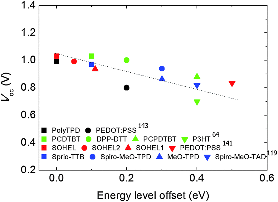 | ||
| Fig. 7 Change in Voc of PHJ PrSCs as a function of the energy level offset between HELs and perovskite. | ||
The use of self-assembling monolayers (SAM) is an effective way to tailor the energy level of a layer; the effect results from the formation of a permanent dipole in the SAM. The deposition of 3-aminopropanoic acid SAM (C3-SAM) onto sol–gel ZnO successfully decreased the WF of ZnO from 4.17 to 3.52 eV, and thereby improved its energy level alignment with the CBM of the MAPbI3 perovskite (3.75 eV).82 As a result, n–i–p PHJ PrSCs with SAM treatment showed a higher Voc (1.07 V) than the reference device (0.99 V) (Fig. 8a). The energy level of sol–gel ZnO was also tuned by deposition of a thin organic surface modifier, PCBM onto it. The deposition of PCBM changed the electronic structure of the ZnO film into a more favourable form.160 In particular, the use of a ZnO/PCBM EEL decreased the energy level offset with the CBM of MAPbI3 and as a result increased the difference in quasi-Fermi levels in a device compared to that in a device with ZnO alone. Therefore, the device with the ZnO/PCBM EEL had a higher Voc (1.02 V) than a device with a ZnO-only EEL (0.78 V) (Fig. 8b). Also, efficient charge transfer and extraction by the favourable energy level alignment increased the Jsc and FF in the device with ITO/ZnO/PCBM/MAPbI3/PTB7-Th/MoO3/Ag; as a result it achieved a PCE = 12.2%.
 | ||
| Fig. 8 J–V characteristics of the PHJ PrSCs with energy level tailored EELs (a) C3-SAM (Reproduced from ref. 82 with permission from the American Chemical Society) (b) PC61BM (Reproduced from ref. 160 with permission from The Royal Society of Chemistry) (c) PEIE and P3TMAHT (Reproduced from ref. 146 with permission from the American Chemical Society) (d) LiF (Reproduced from ref. 147 with permission from The Royal Society of Chemistry). | ||
PC61BM is a representative material as an EEL in p–i–n PHJ PrSCs because it has excellent electron accepting properties.
However, the difference between the lowest unoccupied molecular orbital (LUMO) of PC61BM and WF of the metal contact causes a decrease in the quasi-Fermi level difference and a lower built-in voltage which lead to low device performance. To form a quasi-Ohmic contact between PC61BM and the Ag cathode, PEIE or poly[3-(6-trimethylammoniumhexyl)thiophene] (P3TMAHT) were inserted between the layers (Fig. 8c).146 Both polymers formed interface dipoles with a negative charge on Ag and decreased its WF from 4.7 eV to 3.97 eV (PEIE) and to 4.13 eV (P3TMAHT). The modifying interfacial layers minimized the energy difference between PC61BM and the cathode and maximized the quasi-Fermi level difference in the devices. Hence, the Voc increased from 0.85 V to 0.9 V, and the Jsc and FF were also improved by using the interfacial layers. The device with ITO/PEDOT:PSS/MAPbI3−xClx/PC61BM/PEIE/Ag achieved a PCE = 12.0%, which was higher than the device with a PCE = 8.5% that did not have the interfacial layers. Similarly, a chemisorbed dipolar interface layer, DMAPA-C60 based on an amine functionalized fullerene derivative was used to make a quasi-Ohmic contact between PCBM and the Ag cathode in p–i–n PHJ PrSCs.150 The device structure was ITO/PEDOT:PSS/MAPbI3−xClx/PC61BM/DMAPA-C60/Ag. Owing to the decreased WF of Ag (3.97 eV) with the interfacial layer, the device achieved a PCE = 13.4% with an increased Voc = 0.97 V compared to the device without DMAPA-C60 which had a PCE = 9.4% and Voc = 0.9 V.
A thin LiF layer was also used as an EEL placed between PC61BM and Al in p–i–n PHJ PrSCs.147 The function of the thin metal fluoride layer in this position has been explained in the field of organic solar cells: (1) formation of a dipole to reduce the WF of the metal; (2) reaction with the metal contact to facilitate charge extraction; and (3) decrease in metal-bonding induced damage to PC61BM.161–164 Based on the effects, devices with LiF/Al showed a superior PCE = 13.1% to the device without LiF (11.5%) (Fig. 8d).
In short, Voc strongly depends on the energy level offset at the electrode interfaces. Voc of devices can be increased linearly by using energy-level-tailored HELs and EELs at the interface of PHJ PrSCs. The maximum Voc is achieved when the energy levels of HELs and EELs are pinned to the VBM and CBM of perovskites, respectively. We expect that this review of how Voc depends on the energy-level tailoring of interfacial layers will be helpful to provide an insight into the ways to maximize Voc of devices with various kinds of perovskite light absorbers. More specific information of the HELs and EELs including their characteristics in terms of the energy level and device performance is summarized (Tables 3 and 4). Also, we summarized energy level diagram of the HELs and EELs described in this section (Fig. 9).
| HEL | IE of HEL (eV) | Perovskite | VBM of perovskite (eV) | Offset (eV) | V oc (V) | J sc (mA cm−2) | FF (%) | PCE (%) | Device architecture | Ref. |
|---|---|---|---|---|---|---|---|---|---|---|
| *We surveyed relevant articles that compared HELs in PHJ PrSCs and exhibited energy levels of HELs, perovskites and the corresponding device performance.a PCDTBT: (poly(N-9′-heptadecanyl-2,7-carbazole-alt-5,5-(4′,7′-di(thien-2-yl)-2′,1′,3′-benzothiadiazole))).b DPP-DTT: poly(2,5-(2-di(thien-2-yl)thieno[3,2-b]thiophene)).c PCPDTBT: poly(2,6-(4,4-bis(2-ethylhexyl)-4H-cyclopenta[2,1-b;3,4-b′]dithiophene)-alt-4′,7′-(2′,1′,3′-benzothiadiazole).d P3HT: poly(3-n-hexylthiophene)).e SOHEL: self-organized hole extraction layer.f PEDOT:PSS: poly(3,4-ethylenedioxythiophene) polystyrene sulfonate.g Spiro-TTB:.h Spiro-MeO-TPD:.i MeO-TPD:.j Sprio-MeO-TAD: 2,20,7,70-tetrakis(N,N0-di-p-methoxyphenylamine)-9,90-spirobifluorene poly[3-(6-trimethylammoniumhexyl)thiophene].k Poly-TPD: poly(N,N′-bis(4-butylphenyl-N,N′-bis(phenyl)benzidine)).l PC61BM: [6,6]-phenyl C61 butyric acid methyl ester.m BCP: bathocuproine. | ||||||||||
| PCDTBTa | 5.3 | MAPbI3 | 5.4 | 0.1 | 1.03 | 15.9 | 66 | 10.9 | ITO/PEDOT:PSS/HEL/MAPbI3/PCBMl/LiF/Ag | 64 |
| DPP-DTTb | 5.2 | 0.2 | 1.00 | 13.3 | 74 | 9.8 | ||||
| PCPDTBTc | 5.0 | 0.4 | 0.88 | 13.0 | 69 | 7.8 | ||||
| P3HTd | 5.0 | 0.4 | 0.7 | 14.2 | 78 | 8.5 | ||||
| SOHELe | 5.39 | MAPbI3 | 5.43 | 0.04 | 0.982 | 16.7 | 70.5 | 11.7 | ITO/HEL/MAPbI3/PC61BM/Al | 141 |
| PEDOT:PSSf | 4.9 | 0.53 | 0.835 | 14.1 | 68.5 | 8.1 | ||||
| Spiro-TTBg | 5.3 | MAPbI3−xClx | 5.4 | 0.1 | 0.970 | 14.9 | 63 | 9.1 | ITO/HEL/MAPbI3−xClx/C60/Ag | 119 |
| Sprio-MeO-TPDh | 5.1 | 0.3 | 0.940 | 15.5 | 66 | 9.6 | ||||
| MeO-TPDi | 5.1 | 0.3 | 0.863 | 14.5 | 63 | 7.8 | ||||
| Sprio-MeO-TADj | 5.0 | 0.4 | 0.820 | 14.1 | 63 | 7.2 | ||||
| Poly-TPDk | 5.4 | MAPbI3 | 5.4 | 0 | 0.99 | 20.01 | 69.55 | 13.78 | ITO/HEL/MAPbI3/PC61BM/C60/BCPm/Ag | 143 |
| PEDOT:PSS | 5.2 | 0.2 | 0.80 | 9.41 | 61.80 | 4.63 | ||||
| EEL | LUMO of EEL (eV) | Perovskite | CBM of perovskite (eV) | Offset (eV) | V oc (V) | J sc (mA cm−2) | FF (%) | PCE (%) | Device architecture | Ref. |
|---|---|---|---|---|---|---|---|---|---|---|
| *We surveyed relevant articles that compared EELs in PHJ PrSCs and exhibited energy levels of EELs and perovskites and the corresponding device performance. **Regarding EELs used on the PC61BM layer, the energy level offset was investigated between PC61BM and the electrode.a PC61BM: [6,6]-phenyl C61 butyric acid methyl ester.b IC60BA: indene-C60 bisadduct.c BCP: bathocuproine.d PEIE: poly-(ethyleneimine ethoxylated).e P3TMAHT: poly[3-(6-trimethylammoniumhexyl)thiophene].f DMAPA: dimethylaminopropylamine.g PDINO: perylene-diimide.h TIPD: titanium (diisopropoxide) bis(2,4-pentanedionate).i PTB7-Th: poly[4,8-bis(5-(2-ethylhexyl)thiophen-2-yl)benzo][1,2-b;4,5-b′]dithiophene-2,6-diyl-alt-(4-(2-ethylhexyl)-3-fluorothieno[3,4-b]thiophene-)-2-carboxylate-2-6-diyl. | ||||||||||
| ZnO/PC61BMa | 3.9 | MAPbI3 | 3.7 | 0.2 | 1.02 | 14.73 | 73 | 10.87 | ITO/EEL/MAPbI3/PTB7-Thi/MoO3/Ag | 160 |
| ZnO | 4.2 | 0.5 | 0.78 | 14.54 | 68 | 7.65 | ||||
| IC60BAb/C60/BCPc | 3.7 | MAPbI3 | 3.7 | 0 | 0.98 | 11.3 | 80 | 8.83 | ITO/PEDOT:PSS/MAPbI3/EEL/Al | 22 |
| PC61BM/C60/BCP | 3.9 | 0.2 | 0.82 | 12.4 | 74.1 | 7.53 | ||||
| C60/BCP | 4.5 | 0.8 | 0.53 | 12.2 | 33.1 | 2.14 | ||||
| PEIEd | 3.97 | MAPbI3−xClx | 4.2** | 0 | 0.899 | 17.32 | 77.10 | 12.01 | ITO/PEDOT:PSS/MAPbI3/PC61BM/EEL/Ag | 146 |
| P3TMAHTe | 4.13 | 0.07 | 0.899 | 17.10 | 74.10 | 11.28 | ||||
| Ag only | 4.7 | 0.5 | 0.849 | 16.00 | 60.29 | 8.53 | ||||
| DMAPAf-C60 | 3.97 | MAPbI3−xClx | 3.95** | 0.02 | 0.97 | 17.9 | 77 | 13.4 | ITO/PEDOT:PSS/MAPbI3−xClx/PC61BM/EEL/Ag | 150 |
| Ag only | 4.74 | 0.79 | 0.90 | 17.1 | 61 | 9.4 | ||||
| PDINOg | 3.63 | MAPbI3−xClx | 3.9** | 0 | 0.95 | 18.8 | 78.5 | 14.0 | ITO/PEDOT:PSS/MAPbI3−xClx/PC61BM/EEL/Ag | 153 |
| ZnO | 4.4 | 0.5 | 0.95 | 16.0 | 74.5 | 11.3 | ||||
| Ag only | 4.6 | 0.7 | 0.85 | 17.5 | 67.6 | 10.0 | ||||
| TIPDh | 3.9 | MAPbI3 | 3.9** | 0 | 0.89 | 22.57 | 64.5 | 12.95 | ITO/PEDOT:PSS/MAPbI3/PC61BM/EEL/Al | 157 |
| Al only | 4.3 | 0.4 | 0.83 | 15.42 | 67.7 | 8.66 | ||||
 | ||
| Fig. 9 Energy level diagram of HELs (left) and EELs (right) used in PHJ PrSCs and perovskite light absorbers (middle). The unit for each value is [eV] but omitted. The values of IEs of HELs and EAs of EELs were extracted from the references which are provided in Section 4.1. The energy levels of MAPbI3, MAPbI3−xClx and MAPbBr3 were extracted from ref. 47. The energy level of FAPbI3 was extracted from ref. 196. | ||
4.2. Electrical conductivity of interfacial layers
Electrical conductivity of interfacial layers in PHJ PrSCs is also an important factor determining device performance because charge transport occurs through the interfacial layers from perovskite absorbers. In general, high electrical conductivity of an interfacial layer is favourable so that charges can be efficiently collected to a desired electrode with minimized recombination as long as charge balance between electrons and holes is stable in a device. Although spiro-OMeTAD and PTAA are typically used as hole interfacial layers in n–i–p PHJ PrSCs, they have a low conductivity and low hole mobility in the absence of dopants such as lithium bis(trifluoromethylsulfonyl)-imide (Li-TFSi) and tert-butylpyridine (tBP).165–167 Moreover, the difference in electrical conductivity between the perovskite light absorber and an interfacial layer can cause accumulation of charges at the interface and formation of space charges that can impede efficient charge transfer and transport. Therefore, devices with an undoped HEL showed low PCE.168–172To overcome this limitation, a dopant-free donor–acceptor conjugated small molecule, DOR3T-TBDT, was introduced as a HEL in a n–i–p PHJ device with the ITO/TiO2/MAPbI3−xClx/DOR3T-TBDT/MoO3/Ag structure.81 The bulk electrical conductivity of the HEL measured by a transmission line model at room temperature (RT) was ∼4 × 10⁻⁴ S cm−1 and the hole mobility extracted from organic field-effect transistors (OFETs) was 0.26 cm2 V−1 s−1; both are higher than those of pristine spiro-OMeTAD (conductivity ∼10−5 S cm−2; hole mobility ∼10−4 cm2 V−1 s−1). Electrochemical impedance spectroscopy (EIS) measurements of devices also showed the lower resistance of the DOR3T-TBDT based device than the device with dopant-free spiro-OMeTAD. Moreover, a significant photoluminescence (PL) quenching and shortened PL lifetime of the DOR3T-TBDT interfaced MAPbI3−xClx layer indicated efficient hole extraction. Therefore, the device with DOR3T-TBDT which achieved a higher PCE = 14.9% than the devices with dopant-free spiro-OMeTAD (3.5%).
Another method to increase the low electrical conductivity of pure spiro-OMeTAD is to introduce multi-walled carbon nanotubes (MWNTs) into it.80 Owing to the high carrier mobility (∼220 cm2 V−1 s−1), electrical properties of spiro-OMeTAD that incorporated 0.5 wt% of MWNTs had carrier mobility more than two orders of magnitude larger, and conductivity three orders larger than pristine spiro-OMeTAD. Here, however, the lower WF of MWNTs (4.6 eV) provided a path for undesired electron transfer.173–175 Therefore, a hierarchical structure composed of pure spiro-OMeTAD/spiro-OMeTAD:MWNTs was introduced to block back-electron transfer. The first deposited pure spiro-OMeTAD efficiently blocked back-electron transfer due to its lower LUMO (2.3 eV) than the CBM of MAPbI3 (3.9 eV). As a result of increased electrical conductivity of the MWNT embedded spiro-OMeTAD and efficient blocking of back-electron transfer by pristine spiro-OMeTAD, the device with the FTO/TiO2/MAPbI3/spiro-OMeTAD/spiro-OMeTAD:MWNTs/Au structure achieved a PCE = 15.1% which exceeded the PCE = 12.8% of the device to which MWNTs were not added.
Studies on EELs of p–i–n PHJ PrSCs have also been reported. PCBM, the popular EEL, has been doped with graphdiyne, a novel two-dimensional carbon material.155 While the electron mobility of an unipolar device with pure PCBM was 2.98 × 10⁻⁴ cm2 V−1 s−1, it was increased to 5.32 × 10⁻⁴ cm2 V−1 s−1 in the device that used graphdiyne-doped PC61BM. The improvement in electron mobility resulted from good electrical characteristics of graphdiyne owing to its carbon network structure with delocalized π-systems. In addition, the device with PC61BM:graphdiyne exhibited less charge recombination because of the better coverage of the EEL and the interfacial contact with the perovskite surface than undoped PC61BM. Due to the increased electrical conductivity of the EEL, the device achieved a PCE = 14.8%, which was higher than PCE of the device with pristine PC61BM (13.6%).
The importance of roles of a fullerene-based n-type layer in a p–i–n type PHJ cell was highlighted particularly with respect to electrical conductivity of the materials;151 the authors presented a clear correlation between the charge-transporting properties of EELs (IC60BA, PC61BM and C60) and device performance. Electron mobilities of the fullerene derivatives were obtained from FETs based on each fullerene derivative. The gradual increase in electron mobility from IC60BA (6.9 × 10⁻³ cm2 V−1 s−1), to PC61BM (6.1 × 10⁻² cm2 V−1 s−1), to C60 (1.6 cm2 V−1 s−1) was attributed to increased conjugation and dense packing of C60 owing to the lack of bulky side-chains. Due to this reason, the device with C60 as an ETL achieved the highest Jsc = 21.07 mA cm−2 and PCE = 15.44%; the device with PC61BM had a Jsc = 18.85 mA cm−2 and PCE = 13.37%, and the device with IC60BA had a Jsc = 11.27 mA cm−2 and PCE = 8.06%. These results indicate that an EEL with good electrical conductivity promotes efficient charge transport in a device and increase its PCE.
4.3. Passivation of traps in perovskites
The presence of a large density of traps in perovskite absorbers has been identified as the main origin of large photocurrent hysteresis of PrSCs which hampers accurate evaluation of device performance and degrades device reliability.22,50,51,137,151,176–180 To be specific, the hysteresis comes from the difference in rates of charge trapping and de-trapping depending on the voltage sweep direction and sweep rate. Therefore, decreasing trap density of states (tDOS) is required to eliminate the hysteresis of a device. One way of decreasing tDOS is to fill or passivate the traps by applying an intimate interfacial layer with the perovskite; hysteresis-less PHJ PrSCs have been realized using this approach.22,50,151Huang et al. applied a double fullerene layer (PC61BM/C60) onto an MAPbI3 film.22 Thermal admittance spectroscopy (TAS) analysis confirmed the decrease in tDOS after interfacial layer passivation on the perovskite film. While the device without the interfacial layers had a large tDOS in the range from 1 × 10¹⁷ to 1 × 10¹⁹ m−3 eV−1, the device with the interfacial layers had tDOS about two orders of magnitude less than this. The tDOS was also significantly mitigated by appropriate thermal annealing on PC61BM (100 °C for 45 min) (Fig. 10a).50 The schematic image in Fig. 10b shows that PC61BM passivated the trap states and reduced the surface recombination. The increased surface passivation effect of PC61BM on MAPbI3 was revealed from the blue-shift in PL of the films and the surface passivation effect led to reduced interface recombination, an increased carrier lifetime and increased mobility, thereby yielding a high PCE of around 15%. The excellence of fullerene derivatives in trap passivation of perovskites in PHJ PrSCs has been being reported elsewhere to date.151
 | ||
| Fig. 10 (a) Trap density of states (tDOS) obtained by thermal admittance spectroscopy. (b) A schematic image of the surface recombination reduction by passivating the trap states. Reproduced from ref. 50 with permission from Nature Publishing Group. | ||
4.4. Enhancement in long-term stability of devices
Long-term stability of a device is an essential requirement for commercialization. Although PHJ PrSCs have achieved high PCE near 20%, they have poor long-term stability mainly due to the inherent vulnerability of perovskite light absorbers to moisture and heat. Degradation of perovskites after exposure to moisture and heat can be easily traced in various ways. For example, the color change in perovskite films usually from dark brown to yellow, the change in the XRD peaks of perovskite crystal structures, and decreased intensity of light absorption are observable.181–183The sensitivity of perovskites to moisture imparts an additional function to interfacial layers. An appropriate choice of interfacial layers to sandwich perovskites can protect them from exposure to undesirable environments, and thereby extend the stability of a device.
However, the most popular solution-processable conducting polymer HEL in p–i–n PHJ PrSCs, PEDOT:PSS has disadvantages of hygroscopicity and acidity; these properties can degrade the long-term stability of the devices. Therefore, researchers are seeking a way to improve device stability. Chu et al. introduced solution-processable MoO3 between ITO and PEDOT:PSS, and developed a device that had the ITO/MoO3/PEDOT:PSS/MAPbI3/C60/Bphen/Ag structure.144 The device showed better long-term stability than the device with only PEDOT:PSS. Metal ions released from ITO due to damage by acidic PEDOT:PSS can diffuse into the inner layer of a device and degrade it. However, insertion of MoO3 seems to effectively prevent corrosion of ITO by PEDOT:PSS and consequent generation of undesirable species. After 10 days under ambient conditions, the PCE of the device with MoO3 degraded only 7%, whereas the device with only PEDOT:PSS failed completely. Furthermore, owing to increased hole collection efficiency, the device with MoO3 showed a higher PCE = 12.78% than the device with only PEDOT:PSS HEL (PCE = 9.81%). In another approach, PEDOT:PSS was simply replaced with reduced graphene oxide (rGO) nanosheets as HELs; the replacement increased device stability and PCE at the same time.88 The basic structure of the devices was ITO/HEL/MAPbI3/PC61BM/BCP/Ag. About three times longer half-lifetime of rGO device (∼150 h) than the device with PEDOT:PSS (∼50 h) under ambient conditions was attributed to rGO with nearly neutral properties, unlike PEDOT:PSS, which is acidic. With few surface oxygen functionalities, rGO has inherent passivation ability against moisture and oxygen. Also, the device with rGO achieved a PCE = 10.8%, which was higher than a PCE = 9.14% of the device with PEDOT:PSS. These results were ascribed to the superior charge transport ability due to higher conductivity of rGO than PEDOT:PSS and better-aligned energy levels between rGO and the anode.
5. Flexible perovskite solar cells
PrSCs are promising candidates as power sources. Nevertheless, processability at low T is an essential requirement for the realization of flexible PrSCs; therefore, PHJ PrSCs are suitable for this purpose.Snaith et al. demonstrated flexible p–i–n PHJ PrSCs on PET/ITO substrates (ITO/PEDOT:PSS/MAPbI3−xClx/PCBM/TiOx/Al);105 the devices had a PCE = 6.3% (Fig. 11a and b). Around the same time, Kelly et al. reported flexible n–i–p PHJ PrSCs.73 The devices were completed on PET/ITO substrates as well with the ITO/ZnO/MAPbI3/spiro-OMeTAD/Ag structure. The PCE of the flexible devices was 10.2%. The demonstrations presented development possibility of flexible PHJ PrSCs (Fig. 11c and d).
 | ||
| Fig. 11 (a) Picture of flexible p–i–n PHJ PrSCs. (b) J–V charateristics of the flexible device and the device on a glass substrate. Reproduced from ref. 105 with permission from Nature Publishing Group. (c) A picture of flexible n–i–p PHJ PrSCs. (d) J–V charateristics measured under illumination (red line) and in the dark (black line). Reproduced from ref. 73 with permission from Nature Publishing Group. | ||
Jung et al. demonstrated bendable n–i–p PHJ PrSCs based on PEN/ITO substrates.184 The device structure was PEN/ITO/MAPbI3−xClx/Sprio-OMeTAD/Ag. The authors investigated bending stability of the devices under various bending conditions. The flexible PrSCs showed constant PCE as a function of the bending radius rB from 400 to 4 mm. At rB of 400 and 40 mm the devices remained stable, but at rB of 4 mm the devices showed an abrupt decrease in PCE after several tens of bending cycles. The authors attributed this decrease to brittleness of ITO. Here, the researchers examined the fracture behavior of perovskite films. One perovskite film was deposited on PEN/ITO and the other directly on the PEN substrate. The former had cracks from ITO, but the latter did not have any cracks after bending (Fig. 12a and b). The authors attributed these results to the excellent mechanical properties of perovskite films and their compatibility with flexible devices. On the other hand, Kelly et al. reported that repeated bending of the device at a low radius (4 mm) of curvature caused small cracks in the perovskite films. (Fig. 12c and d).185 Nevertheless, the authors concluded that perovskites can tolerate moderate conditions such as roll-to-roll manufacturing. Based on these conflicting conclusions, it is worth studying in-depth and further debating on the flexibility and mechanical durability of perovskite films.
 | ||
| Fig. 12 SEM images of (a) PEN/ITO/TiOx/ and (b) PEN/TiOx/perovskites showing perovskites and their junction parts after 300 bending cycles. Scale bar represents 100 μm. Low-magnification and high-magnification (inset) SEM images of (c) PET/highly conductive PEDOT and (d) PET/highly conductive PEDOT/semiconducting PEDOT/perovskite after 2000 bending cycles. (a) and (b) are reproduced from ref. 184 and (c) and (d) are reproduced from ref. 185 with permission from The Royal Society of Chemistry. | ||
The brittleness of FTO and ITO limits the development of flexible PrSCs. Therefore, finding a way to replace the conventional FTO and ITO electrodes with a transparent flexible electrode is a major requirement for development of flexible PrSCs. Although several papers have reported PrSCs that use flexible transparent conducting electrodes (e.g., aluminum-doped ZnO (AZO)/Ag/AZO and PEDOT:PSS) instead of FTO or ITO, PCEs of the flexible devices were lower than rigid devices due to inferior electrical and optical properties of flexible electrodes.185–187 Therefore, various kinds of flexible transparent conducting electrodes (e.g., PEDOT:PSS, graphene,188,189 carbon nanotubes189 and silver nanowires190) should be vigorously studied with the goal of enhancing compatibility with flexible PrSCs to replace conventional metal oxide brittle electrodes.
6. Conclusions and outlook
We have discussed and pointed out progress in PHJ PrSCs and several strategies for providing insights into interfacial layer engineering to improve photovoltaic performance and stability of PHJ PrSCs.Importantly, improvement of PCE and stability of PHJ PrSCs requires the use of appropriate interfacial layers because the interfacial layers have crucial roles in PHJ PrSCs; (1) proper energy-level tailoring can reduce the energy offset between intimate layers, and thereby increase the built-in potential, and facilitate charge transfer and extraction; (2) electrical conductivity of the interfacial layers strongly affects charge transport properties and efficiency of charge collection; (3) passivation of electronic trap sites in perovskite films can eliminate photocurrent hysteresis; (4) protection of perovskites from moisture improves long-term stability. On the basis of various functions and optimization with comprehensive understanding of interfacial layers, PHJ PrSCs are expected to be further improved in PCE and long-term stability. Obviously, to develop highly efficient flexible PHJ PrSCs, we also need to understand the failure mechanism of the devices against mechanical stress, and adopt a transparent conducting flexible electrode that has excellent electrical, optical, and mechanical properties.
Because one of the ultimate goals of research on PrSCs is to make them ubiquitous in everyday life, manufacturing cost in addition to flexibility should be considered. To meet these requirements, we suggest that p–i–n type PHJ PrSCs are more promising than the n–i–p type, because the structure of, p–i–n type PHJ PrSCs can be further simplified. Specifically, PEDOT:PSS, a representative HEL for p–i–n type PHJ PrSCs, can be modified to have great electrical conductivity (∼4000 S cm−1)193 and a wide range of WF (4.8–5.9 eV)6,141,194 by appropriate chemical treatment. With this adjustability, PEDOT:PSS can concurrently perform both charge extraction and collection in a simple integrated single layer in p–i–n type PHJ PrSCs. Secondly, all-solution-processed flexible PrSCs are achievable because PEDOT:PSS is solution processable and a film of PEDOT:PSS is flexible, whereas conventional metal oxide electrodes (e.g., ITO and FTO) are fabricated by vacuum processing, and are brittle. Therefore, flexible p–i–n type PHJ PrSCs can be fabricated by all-solution roll-to-roll processing. In summary, we expect that p–i–n type PHJ PrSCs can have advantages of the structure and processing over the n–i–p type, and that these advantages will lead to cost-effective fabrication and wide use. However, the stability of PEDOT:PSS is a critical limitation. We believe that this problem can be solved by using various types of fluorinated conducting polymers.6,141,194,195
Acknowledgements
This work was supported by the Center for Advanced Soft-Electronics funded by the Ministry of Science, ICT and Future Planning as Global Frontier Project (CASE-2014M3A6A5060947). This work was also supported by POSCO.References
- H.-S. Kim, C.-R. Lee, J.-H. Im, K.-B. Lee, T. Moehl, A. Marchioro, S.-J. Moon, R. Humphry-Baker, J.-H. Yum, J. E. Moser, M. Grätzel and N.-G. Park, Sci. Rep., 2012, 2, 591 Search PubMed.
- S. D. Stranks, G. E. Eperon, G. Grancini, C. Menelaou, M. J. P. Alcocer, T. Leijtens, L. M. Herz, A. Petrozza and H. J. Snaith, Science, 2013, 342, 341–344 CrossRef CAS PubMed.
- J. Burschka, N. Pellet, S.-J. Moon, R. Humphry-Baker, P. Gao, M. K. Nazeeruddin, M. Grätzel and M. Gratzel, Nature, 2013, 499, 316–319 CrossRef CAS PubMed.
- W. S. Yang, J. H. Noh, N. J. Jeon, Y. C. Kim, S. Ryu, J. Seo and S. Il Seok, Science, 2015, 348, 1234–1237 CrossRef CAS PubMed.
- Z.-K. Tan, R. S. Moghaddam, M. L. Lai, P. Docampo, R. Higler, F. Deschler, M. Price, A. Sadhanala, L. M. Pazos, D. Credgington, F. Hanusch, T. Bein, H. J. Snaith and R. H. Friend, Nat. Nanotechnol., 2014, 9, 687–692 CrossRef CAS PubMed.
- Y.-H. Kim, H. Cho, J. H. Heo, T.-S. Kim, N. Myoung, C.-L. Lee, S. H. Im and T.-W. Lee, Adv. Mater., 2015, 27, 1248–1254 CrossRef CAS PubMed.
- J. C. Yu, D. Bin Kim, G. Baek, B. R. Lee, E. D. Jung, S. Lee, J. H. Chu, D.-K. Lee, K. J. Choi, S. Cho and M. H. Song, Adv. Mater., 2015, 27, 3492–3500 CrossRef CAS PubMed.
- L. Dou, Y. (Micheal) Yang, J. You, Z. Hong, W.-H. Chang, G. Li and Y. Yang, Nat. Commun., 2014, 5, 5404 CrossRef CAS PubMed.
- Y. Lee, J. Kwon, E. Hwang, C.-H. Ra, W. J. Yoo, J.-H. Ahn, J. H. Park and J. H. Cho, Adv. Mater., 2015, 27, 41–46 CrossRef CAS PubMed.
- Q. Lin, A. Armin, D. M. Lyons, P. L. Burn and P. Meredith, Adv. Mater., 2015, 27, 2060–2064 CrossRef CAS PubMed.
- H. Zhu, Y. Fu, F. Meng, X. Wu, Z. Gong, Q. Ding, M. V Gustafsson, M. T. Trinh, S. Jin and X.-Y. Zhu, Nat. Mater., 2015, 14, 636–642 CrossRef CAS PubMed.
- F. Deschler, M. Price, S. Pathak, L. E. Klintberg, D.-D. Jarausch, R. Higler, S. Hüttner, T. Leijtens, S. D. Stranks, H. J. Snaith, M. Atatüre, R. T. Phillips and R. H. Friend, J. Phys. Chem. Lett., 2014, 5, 1421–1426 CrossRef CAS PubMed.
- G. Xing, N. Mathews, S. S. Lim, N. Yantara, X. Liu, D. Sabba, M. Grätzel, S. Mhaisalkar and T. C. Sum, Nat. Mater., 2014, 13, 476–480 CrossRef CAS PubMed.
- A. Kojima, K. Teshima, Y. Shirai and T. Miyasaka, J. Am. Chem. Soc., 2009, 131, 6050–6051 CrossRef CAS PubMed.
- B. O'Regan and M. Gratzel, Nature, 1991, 353, 737–740 CrossRef.
- Y.-H. Kim, I.-K. Lee, Y.-S. Song, M.-H. Lee, B.-Y. Kim, N.-I. Cho and D. Lee, Electron. Mater. Lett., 2014, 10, 445–449 CrossRef CAS.
- J. Park and M. Lee, Electron. Mater. Lett., 2015, 11, 271–275 CrossRef CAS.
- J.-H. Im, C.-R. Lee, J.-W. Lee, S.-W. Park and N.-G. Park, Nanoscale, 2011, 3, 4088–4093 RSC.
- H. Zhou, Q. Chen, G. Li, S. Luo, T. Song, H.-S. Duan, Z. Hong, J. You, Y. Liu and Y. Yang, Science, 2014, 345, 542–546 CrossRef CAS PubMed.
- P.-W. Liang, C.-Y. Liao, C.-C. Chueh, F. Zuo, S. T. Williams, X.-K. Xin, J. Lin and A. K.-Y. Jen, Adv. Mater., 2014, 26, 3748–3754 CrossRef CAS PubMed.
- Z. Xiao, C. Bi, Y. Shao, Q. Dong, Q. Wang, Y. Yuan, C. Wang, Y. Gao and J. Huang, Energy Environ. Sci., 2014, 7, 2619–2623 CAS.
- Q. Wang, Y. Shao, Q. Dong, Z. Xiao, Y. Yuan and J. Huang, Energy Environ. Sci., 2014, 7, 2359–2365 CAS.
- C.-C. Chueh, C.-Y. Liao, F. Zuo, S. T. Williams, P.-W. Liang and A. K.-Y. Jen, J. Mater. Chem. A, 2015, 3, 9058–9062 CAS.
- C. Bi, Y. Shao, Y. Yuan, Z. Xiao, C. Wang, Y. Gao and J. Huang, J. Mater. Chem. A, 2014, 2, 18508–18514 CAS.
- Z. Xiao, Q. Dong, C. Bi, Y. Shao, Y. Yuan and J. Huang, Adv. Mater., 2014, 26, 6503–6509 CrossRef CAS PubMed.
- C. Zuo and L. Ding, Nanoscale, 2014, 6, 9935–9938 RSC.
- H.-B. Kim, H. Choi, J. Jeong, S. Kim, B. Walker, S. Song and J. Y. Kim, Nanoscale, 2014, 6, 6679–6683 RSC.
- H.-L. Hsu, C.-P. Chen, J.-Y. Chang, Y.-Y. Yu and Y.-K. Shen, Nanoscale, 2014, 6, 10281–10288 RSC.
- J. W. Jung, S. T. Williams and A. K.-Y. Jen, RSC Adv., 2014, 4, 62971–62977 RSC.
- F. X. Xie, D. Zhang, H. Su, X. Ren, K. S. Wong, M. Grätzel and W. C. H. Choy, ACS Nano, 2015, 9, 639–646 CrossRef CAS PubMed.
- P.-W. Liang, C.-C. Chueh, X.-K. Xin, F. Zuo, S. T. Williams, C.-Y. Liao and A. K.-Y. Jen, Adv. Energy Mater., 2015, 5, 1400960 Search PubMed.
- Y. Chen, T. Chen and L. Dai, Adv. Mater., 2015, 27, 1053–1059 CrossRef CAS PubMed.
- X. Song, W. Wang, P. Sun, W. Ma and Z.-K. Chen, Appl. Phys. Lett., 2015, 106, 033901 CrossRef.
- H.-L. Hsu, C.-C. Chang, C.-P. Chen, B.-H. Jiang, R.-J. Jeng and C.-H. Cheng, J. Mater. Chem. A, 2015, 3, 9271–9277 CAS.
- T.-B. Song, Q. Chen, H. Zhou, S. Luo, Y. (Michael) Yang, J. You and Y. Yang, Nano Energy, 2015, 12, 494–500 CrossRef CAS.
- D. Wang, Z. Liu, Z. Zhou, H. Zhu, Y. Zhou, C. Huang, Z. Wang, H. Xu, Y. Jin, B. Fan, S. Pang and G. Cui, Chem. Mater., 2014, 26, 7145–7150 CrossRef CAS.
- R. Kang, J.-E. Kim, J.-S. Yeo, S. Lee, Y.-J. Jeon and D.-Y. Kim, J. Phys. Chem. C, 2014, 118, 26513–26520 CAS.
- Y. Chen, Y. Zhao and Z. Liang, Chem. Mater., 2015, 27, 1448–1451 CrossRef CAS.
- L. Q. Zhang, X. W. Zhang, Z. G. Yin, Q. Jiang, X. Liu, J. H. Meng, Y. J. Zhao and H. L. Wang, J. Mater. Chem. A, 2015, 3, 12133–12138 CAS.
- J. Lian, Q. Wang, Y. Yuan, Y. Shao and J. Huang, J. Mater. Chem. A, 2015, 3, 9146–9151 CAS.
- K. Wang, C. Liu, P. Du, L. Chen, J. Zhu, A. Karim and X. Gong, Org. Electron., 2015, 21, 19–26 CrossRef CAS.
- J. Xiong, B. Yang, R. Wu, C. Cao, Y. Huang, C. Liu, Z. Hu, H. Huang, Y. Gao and J. Yang, Org. Electron., 2015, 24, 106–112 CrossRef CAS.
- X. Wang, X. Li, G. Tang, L. Zhao, W. Zhang, T. Jiu and J. Fang, Org. Electron., 2015, 24, 205–211 CrossRef CAS.
- Z. Liu and E.-C. Lee, Org. Electron., 2015, 24, 101–105 CrossRef CAS.
- K. Wang, C. Liu, P. Du, H.-L. Zhang and X. Gong, Small, 2015, 11, 3369–3376 CrossRef CAS PubMed.
- W. Nie, H. Tsai, R. Asadpour, J.-C. Blancon, A. J. Neukirch, G. Gupta, J. J. Crochet, M. Chhowalla, S. Tretiak, M. A. Alam, H.-L. Wang and A. D. Mohite, Science, 2015, 347, 522–525 CrossRef CAS PubMed.
- P. Schulz, E. Edri, S. Kirmayer, G. Hodes, D. Cahen and A. Kahn, Energy Environ. Sci., 2014, 7, 1377–1381 CAS.
- Q.-K. Wang, R.-B. Wang, P.-F. Shen, C. Li, Y.-Q. Li, L.-J. Liu, S. Duhm and J.-X. Tang, Adv. Mater. Interfaces, 2015, 2, 1400528 Search PubMed.
- P. Schulz, L. L. Whittaker-Brooks, B. A. MacLeod, D. C. Olson, Y.-L. Loo and A. Kahn, Adv. Mater. Interfaces, 2015, 2, 1400532 Search PubMed.
- Y. Shao, Z. Xiao, C. Bi, Y. Yuan and J. Huang, Nat. Commun., 2014, 5, 5784 CrossRef CAS PubMed.
- N. K. Noel, A. Abate, S. D. Stranks, E. S. Parrott, V. M. Burlakov, A. Goriely and H. J. Snaith, ACS Nano, 2014, 8, 9815–9821 CrossRef CAS PubMed.
- T. Leijtens, S. D. Stranks, G. E. Eperon, R. Lindblad, E. M. J. Johansson, I. J. McPherson, H. Rensmo, J. M. Ball, M. M. Lee and H. J. Snaith, ACS Nano, 2014, 8, 7147–7155 CrossRef CAS PubMed.
- A. Baumann, S. Väth, P. Rieder, M. C. Heiber, K. Tvingstedt and V. Dyakonov, J. Phys. Chem. Lett., 2015, 6, 2350–2354 CrossRef CAS PubMed.
- G.-J. A. H. Wetzelaer, M. Scheepers, A. M. Sempere, C. Momblona, J. Ávila and H. J. Bolink, Adv. Mater., 2015, 27, 1837–1841 CrossRef CAS PubMed.
- D. B. Mitzi, C. A. Feild, W. T. A. Harrison and A. M. Guloy, Nature, 1994, 369, 467–469 CrossRef CAS.
- V. M. Goldschmidt, Naturwissenschaften, 1926, 14, 477–485 CrossRef CAS.
- C. Li, X. Lu, W. Ding, L. Feng, Y. Gao and Z. Guo, Acta Crystallogr. Sect. B: Struct. Sci., 2008, 64, 702–707 CrossRef CAS PubMed.
- K. Tanaka, T. Takahashi, T. Ban, T. Kondo, K. Uchida and N. Miura, Solid State Commun., 2003, 127, 619–623 CrossRef CAS.
- M. Hirasawa, T. Ishihara, T. Goto, K. Uchida and N. Miura, Phys. B, 1994, 201, 427–430 CrossRef CAS.
- T. Ishihara, J. Lumin., 1994, 60–61, 269–274 CrossRef CAS.
- I. B. Koutselas, L. Ducasse and G. C. Papavassiliou, J. Phys.: Condens. Matter, 1996, 8, 1217–1227 CrossRef CAS.
- W. Zhang, M. Saliba, S. D. Stranks, Y. Sun, X. Shi, U. Wiesner and H. J. Snaith, Nano Lett., 2013, 13, 4505–4510 CrossRef CAS PubMed.
- V. D'Innocenzo, G. Grancini, M. J. P. Alcocer, A. R. S. Kandada, S. D. Stranks, M. M. Lee, G. Lanzani, H. J. Snaith and A. Petrozza, Nat. Commun., 2014, 5, 3586 Search PubMed.
- Q. Lin, A. Armin, R. C. R. Nagiri, P. L. Burn and P. Meredith, Nat. Photonics, 2015, 9, 106–112 CrossRef CAS.
- J. H. Heo, S. H. Im, J. H. Noh, T. N. Mandal, C.-S. Lim, J. A. Chang, Y. H. Lee, H. Kim, A. Sarkar, K. Nazeeruddin, M. Gratzel and S. Il Seok, Nat. Photonics, 2013, 7, 486–491 CrossRef CAS.
- H. J. Snaith, J. Phys. Chem. Lett., 2013, 4, 3623–3630 CrossRef CAS.
- N. J. Jeon, J. H. Noh, Y. C. Kim, W. S. Yang, S. Ryu and S. Il Seok, Nat. Mater., 2014, 13, 897–903 CrossRef CAS PubMed.
- J. M. Ball, M. M. Lee, A. Hey and H. J. Snaith, Energy Environ. Sci., 2013, 6, 1739–1743 CAS.
- D. Liu, M. K. Gangishetty and T. L. Kelly, J. Mater. Chem. A, 2014, 2, 19873–19881 CAS.
- B. Conings, L. Baeten, T. Jacobs, R. Dera, J. D'Haen, J. Manca and H.-G. Boyen, APL Mater., 2014, 2, 081505 CrossRef.
- J. Song, E. Zheng, J. Bian, X.-F. Wang, W. Tian, Y. Sanehira and T. Miyasaka, J. Mater. Chem. A, 2015, 3, 10837–10844 CAS.
- C.-Y. Chang, C.-Y. Chu, Y.-C. Huang, C.-W. Huang, S.-Y. Chang, C.-A. Chen, C.-Y. Chao and W.-F. Su, ACS Appl. Mater. Interfaces, 2015, 7, 4955–4961 CAS.
- D. Liu and T. L. Kelly, Nat. Photonics, 2014, 8, 133–138 CrossRef CAS.
- L. Wang, W. Fu, Z. Gu, C. Fan, X. Yang, H. Li and H. Chen, J. Mater. Chem. C, 2014, 2, 9087–9090 RSC.
- S. Ryu, J. Seo, S. S. Shin, Y. C. Kim, N. J. Jeon, J. H. Noh and S. Il Seok, J. Mater. Chem. A, 2015, 3, 3271–3275 CAS.
- H.-H. Wang, Q. Chen, H. Zhou, L. Song, Z. S. Louis, N. De Marco, Y. Fang, P. Sun, T.-B. Song, H. Chen and Y. Yang, J. Mater. Chem. A, 2015, 3, 9108–9115 CAS.
- H. Zhou, Y. Shi, K. Wang, Q. Dong, X. Bai, Y. Xing, Y. Du and T. Ma, J. Phys. Chem. C, 2015, 119, 4600–4605 CAS.
- A. Yella, L.-P. Heiniger, P. Gao, M. K. Nazeeruddin and M. Grätzel, Nano Lett., 2014, 14, 2591–2596 CrossRef CAS PubMed.
- K. Wang, Y. Shi, Q. Dong, Y. Li, S. Wang, X. Yu, M. Wu and T. Ma, J. Phys. Chem. Lett., 2015, 6, 755–759 CrossRef CAS PubMed.
- J. Lee, M. M. Menamparambath, J.-Y. Hwang and S. Baik, ChemSusChem, 2015, 8, 2358–2362 CrossRef CAS PubMed.
- Y. Liu, Q. Chen, H.-S. Duan, H. Zhou, Y. (Michael) Yang, H. Chen, S. Luo, T.-B. Song, L. Dou, Z. Hong and Y. Yang, J. Mater. Chem. A, 2015, 3, 11940–11947 CAS.
- L. Zuo, Z. Gu, T. Ye, W. Fu, G. Wu, H. Li and H. Chen, J. Am. Chem. Soc., 2015, 137, 2674–2679 CrossRef CAS PubMed.
- J.-Y. Jeng, Y.-F. Chiang, M.-H. Lee, S.-R. Peng, T.-F. Guo, P. Chen and T.-C. Wen, Adv. Mater., 2013, 25, 3727–3732 CrossRef CAS PubMed.
- L. Etgar, P. Gao, Z. Xue, Q. Peng, A. K. Chandiran, B. Liu, M. K. Nazeeruddin and M. Grätzel, J. Am. Chem. Soc., 2012, 134, 17396–17399 CrossRef CAS PubMed.
- K.-C. Wang, J.-Y. Jeng, P.-S. Shen, Y.-C. Chang, E. W.-G. Diau, C.-H. Tsai, T.-Y. Chao, H.-C. Hsu, P.-Y. Lin, P. Chen, T.-F. Guo and T.-C. Wen, Sci. Rep., 2014, 4, 4756 Search PubMed.
- S. Ye, W. Sun, Y. Li, W. Yan, H. Peng, Z. Bian, Z. Liu and C. Huang, Nano Lett., 2015, 15, 3723–3728 CrossRef CAS PubMed.
- Z. Wu, S. Bai, J. Xiang, Z. Yuan, Y. Yang, W. Cui, X. Gao, Z. Liu, Y. Jin and B. Sun, Nanoscale, 2014, 6, 10505–10510 RSC.
- J.-S. Yeo, R. Kang, S. Lee, Y.-J. Jeon, N. Myoung, C.-L. Lee, D.-Y. Kim, J.-M. Yun, Y.-H. Seo, S.-S. Kim and S.-I. Na, Nano Energy, 2015, 12, 96–104 CrossRef CAS.
- B. Conings, L. Baeten, C. De Dobbelaere, J. D'Haen, J. Manca and H.-G. Boyen, Adv. Mater., 2014, 26, 2041–2046 CrossRef CAS PubMed.
- Q. Chen, H. Zhou, Z. Hong, S. Luo, H.-S. Duan, H.-H. Wang, Y. Liu, G. Li and Y. Yang, J. Am. Chem. Soc., 2014, 136, 622–625 CrossRef CAS PubMed.
- G. E. Eperon, S. D. Stranks, C. Menelaou, M. B. Johnston, L. M. Herz and H. J. Snaith, Energy Environ. Sci., 2014, 7, 982–988 CAS.
- M. Xiao, F. Huang, W. Huang, Y. Dkhissi, Y. Zhu, J. Etheridge, A. Gray-Weale, U. Bach, Y.-B. Cheng and L. Spiccia, Angew. Chem., 2014, 126, 10056–10061 CrossRef.
- Y. Wu, A. Islam, X. Yang, C. Qin, J. Liu, K. Zhang, W. Peng and L. Han, Energy Environ. Sci., 2014, 7, 2934–2938 CAS.
- J. H. Heo, D. H. Song and S. H. Im, Adv. Mater., 2014, 26, 8179–8183 CrossRef CAS PubMed.
- P. Docampo, F. C. Hanusch, S. D. Stranks, M. Döblinger, J. M. Feckl, M. Ehrensperger, N. K. Minar, M. B. Johnston, H. J. Snaith and T. Bein, Adv. Energy Mater., 2014, 4, 1400355 Search PubMed.
- Y. Zhao and K. Zhu, J. Am. Chem. Soc., 2014, 136, 12241–12244 CrossRef CAS PubMed.
- Y. Guo, C. Liu, K. Inoue, K. Harano, H. Tanaka and E. Nakamura, J. Mater. Chem. A, 2014, 2, 13827–13830 CAS.
- M. Saliba, K. W. Tan, H. Sai, D. T. Moore, T. Scott, W. Zhang, L. A. Estroff, U. Wiesner and H. J. Snaith, J. Phys. Chem. C, 2014, 118, 17171–17177 CAS.
- F. C. Hanusch, E. Wiesenmayer, E. Mankel, A. Binek, P. Angloher, C. Fraunhofer, N. Giesbrecht, J. M. Feckl, W. Jaegermann, D. Johrendt, T. Bein and P. Docampo, J. Phys. Chem. Lett., 2014, 5, 2791–2795 CrossRef CAS PubMed.
- Q. Chen, H. Zhou, T.-B. Song, S. Luo, Z. Hong, H.-S. Duan, L. Dou, Y. Liu and Y. Yang, Nano Lett., 2014, 14, 4158–4163 CrossRef CAS PubMed.
- Z. Ren, A. Ng, Q. Shen, H. C. Gokkaya, J. Wang, L. Yang, W.-K. Yiu, G. Bai, A. B. Djuriić, W. W. Leung, J. Hao, W. K. Chan and C. Surya, Sci. Rep., 2014, 4, 6752 CrossRef PubMed.
- J. H. Heo, D. H. Song, H. J. Han, S. Y. Kim, J. H. Kim, D. Kim, H. W. Shin, T. K. Ahn, C. Wolf, T.-W. Lee and S. H. Im, Adv. Mater., 2015, 27, 3424–3430 CrossRef CAS PubMed.
- Y. Zhou, M. Yang, W. Wu, A. L. Vasiliev, K. Zhu and N. P. Padture, J. Mater. Chem. A, 2015, 3, 8178–8184 CAS.
- W. Zhang, M. Saliba, D. T. Moore, S. K. Pathak, M. T. Hörantner, T. Stergiopoulos, S. D. Stranks, G. E. Eperon, J. A. Alexander-Webber, A. Abate, A. Sadhanala, S. Yao, Y. Chen, R. H. Friend, L. A. Estroff, U. Wiesner and H. J. Snaith, Nat. Commun., 2015, 6, 6142 CrossRef CAS PubMed.
- P. Docampo, J. M. Ball, M. Darwich, G. E. Eperon and H. J. Snaith, Nat. Commun., 2013, 4, 2761 Search PubMed.
- J. You, Z. Hong, Y. (Michael) Yang, Q. Chen, M. Cai, T.-B. Song, C.-C. Chen, S. Lu, Y. Liu, H. Zhou and Y. Yang, ACS Nano, 2014, 8, 1674–1680 CrossRef CAS PubMed.
- J. You, Y. (Michael) Yang, Z. Hong, T.-B. Song, L. Meng, Y. Liu, C. Jiang, H. Zhou, W.-H. Chang, G. Li and Y. Yang, Appl. Phys. Lett., 2014, 105, 183902 CrossRef.
- C.-H. Chiang, Z.-L. Tseng and C.-G. Wu, J. Mater. Chem. A, 2014, 2, 15897–15903 CAS.
- Y. Rong, Z. Tang, Y. Zhao, X. Zhong, S. Venkatesan, H. Graham, M. Patton, Y. Jing, A. M. Guloy and Y. Yao, Nanoscale, 2015, 7, 10595–10599 RSC.
- Q. Xue, Z. Hu, C. Sun, Z. Chen, F. Huang, H.-L. Yip and Y. Cao, RSC Adv., 2015, 5, 775–783 RSC.
- F. Zuo, S. T. Williams, P.-W. Liang, C.-C. Chueh, C.-Y. Liao and A. K.-Y. Jen, Adv. Mater., 2014, 26, 6454–6460 CrossRef CAS PubMed.
- H. Choi, J. Jeong, H.-B. Kim, S. Kim, B. Walker, G.-H. Kim and J. Y. Kim, Nano Energy, 2014, 7, 80–85 CrossRef CAS.
- Z. Cheng and J. Lin, CrystEngComm, 2010, 12, 2646–2662 RSC.
- J. H. Noh, S. H. Im, J. H. Heo, T. N. Mandal and S. Il Seok, Nano Lett., 2013, 13, 1764–1769 CrossRef CAS PubMed.
- J. A. Christians, P. A. Miranda Herrera and P. V Kamat, J. Am. Chem. Soc., 2015, 137, 1530–1538 CrossRef CAS PubMed.
- J. M. Frost, K. T. Butler, F. Brivio, C. H. Hendon, M. van Schilfgaarde and A. Walsh, Nano Lett., 2014, 14, 2584–2590 CrossRef CAS PubMed.
- M. Liu, M. B. Johnston and H. J. Snaith, Nature, 2013, 501, 395–398 CrossRef CAS PubMed.
- O. Malinkiewicz, A. Yella, Y. H. Lee, G. M. Espallargas, M. Graetzel, M. K. Nazeeruddin and H. J. Bolink, Nat. Photonics, 2014, 8, 128–132 CrossRef CAS.
- L. E. Polander, P. Pahner, M. Schwarze, M. Saalfrank, C. Koerner and K. Leo, APL Mater., 2014, 2, 081503 CrossRef.
- T.-W. Lee, T. Noh, H.-W. Shin, O. Kwon, J.-J. Park, B.-K. Choi, M.-S. Kim, D. W. Shin and Y.-R. Kim, Adv. Funct. Mater., 2009, 19, 1625–1630 CrossRef CAS.
- B.-S. Kim, T.-M. Kim, M.-S. Choi, H.-S. Shim and J.-J. Kim, Org. Electron., 2015, 17, 102–106 CrossRef CAS.
- T.-W. Lee, K.-G. Lim and D.-H. Kim, Electron. Mater. Lett., 2010, 6, 41–50 CrossRef CAS.
- J. H. Park, T.-W. Lee, B.-D. Chin, D. H. Wang and O. O. Park, Macromol. Rapid Commun., 2010, 31, 2095–2108 CrossRef CAS PubMed.
- D.-H. Kim, K.-G. Lim, J. H. Park and T.-W. Lee, ChemSusChem, 2012, 5, 2053–2057 CrossRef CAS PubMed.
- S. D. Stranks, V. M. Burlakov, T. Leijtens, J. M. Ball, A. Goriely and H. J. Snaith, Phys. Rev. Appl., 2014, 2, 034007 CrossRef.
- E. Edri, S. Kirmayer, D. Cahen and G. Hodes, J. Phys. Chem. Lett., 2013, 4, 897–902 Search PubMed.
- D. Bi, S.-J. Moon, L. Haggman, G. Boschloo, L. Yang, E. M. J. Johansson, M. K. Nazeeruddin, M. Gratzel and A. Hagfeldt, RSC Adv., 2013, 3, 18762–18766 RSC.
- S. Ryu, J. H. Noh, N. J. Jeon, Y. Chan Kim, W. S. Yang, J. Seo and S. Il Seok, Energy Environ. Sci., 2014, 7, 2614–2618 CAS.
- B. Cai, Y. Xing, Z. Yang, W.-H. Zhang and J. Qiu, Energy Environ. Sci., 2013, 6, 1480–1485 CAS.
- L. Yang, U. B. Cappel, E. L. Unger, M. Karlsson, K. M. Karlsson, E. Gabrielsson, L. Sun, G. Boschloo, A. Hagfeldt and E. M. J. Johansson, Phys. Chem. Chem. Phys., 2012, 14, 779–789 RSC.
- C. Liu, K. Wang, P. Du, T. Meng, X. Yu, S. Z. D. Cheng and X. Gong, ACS Appl. Mater. Interfaces, 2015, 7, 1153–1159 CAS.
- A. T. Barrows, A. J. Pearson, C. K. Kwak, A. D. F. Dunbar, A. R. Buckley and D. G. Lidzey, Energy Environ. Sci., 2014, 7, 2944–2950 CAS.
- S. Sun, T. Salim, N. Mathews, M. Duchamp, C. Boothroyd, G. Xing, T. C. Sum and Y. M. Lam, Energy Environ. Sci., 2014, 7, 399–407 CAS.
- S. Paek, N. Cho, H. Choi, H. Jeong, J. S. Lim, J.-Y. Hwang, J. K. Lee and J. Ko, J. Phys. Chem. C, 2014, 118, 25899–25905 CAS.
- J. H. Kim, S. T. Williams, N. Cho, C.-C. Chueh and A. K.-Y. Jen, Adv. Energy Mater., 2015, 5, 1401229 Search PubMed.
- M. Ramesh, K. M. Boopathi, T.-Y. Huang, Y.-C. Huang, C.-S. Tsao and C.-W. Chu, ACS Appl. Mater. Interfaces, 2015, 7, 2359–2366 CAS.
- J. H. Heo, H. J. Han, D. Kim, T. K. Ahn and S. H. Im, Energy Environ. Sci., 2015, 8, 1602–1608 CAS.
- N. Tripathi, M. Yanagida, Y. Shirai, T. Masuda, L. Han and K. Miyano, J. Mater. Chem. A, 2015, 3, 12081–12088 CAS.
- K. M. Boopathi, M. Ramesh, P. Perumal, Y.-C. Huang, C.-S. Tsao, Y.-F. Chen, C.-H. Lee and C.-W. Chu, J. Mater. Chem. A, 2015, 3, 9257–9263 CAS.
- H.-L. Hsu, T.-Y. Juang, C.-P. Chen, C.-M. Hsieh, C.-C. Yang, C.-L. Huang and R.-J. Jeng, Sol. Energy Mater. Sol. Cells, 2015, 140, 224–231 CrossRef CAS.
- K.-G. Lim, H.-B. Kim, J. Jeong, H. Kim, J. Y. Kim and T.-W. Lee, Adv. Mater., 2014, 26, 6461–6466 CrossRef CAS PubMed.
- W. Yan, Y. Li, W. Sun, H. Peng, S. Ye, Z. Liu, Z. Bian and C. Huang, RSC Adv., 2014, 4, 33039–33046 RSC.
- D. Zhao, M. Sexton, H.-Y. Park, G. Baure, J. C. Nino and F. So, Adv. Energy Mater., 2015, 5, 1401855 Search PubMed.
- F. Hou, Z. Su, F. Jin, X. Yan, L. Wang, H. Zhao, J. Zhu, B. Chu and W. Li, Nanoscale, 2015, 7, 9427–9432 RSC.
- M. Qian, M. Li, X.-B. Shi, H. Ma, Z.-K. Wang and L.-S. Liao, J. Mater. Chem. A, 2015, 3, 13533–13539 CAS.
- H. Zhang, H. Azimi, Y. Hou, T. Ameri, T. Przybilla, E. Spiecker, M. Kraft, U. Scherf and C. J. Brabec, Chem. Mater., 2014, 26, 5190–5193 CrossRef CAS.
- J. Seo, S. Park, Y. Chan Kim, N. J. Jeon, J. H. Noh, S. C. Yoon and S. Il Seok, Energy Environ. Sci., 2014, 7, 2642–2646 CAS.
- Q. Xue, Z. Hu, J. Liu, J. Lin, C. Sun, Z. Chen, C. Duan, J. Wang, C. Liao, W. M. Lau, F. Huang, H.-L. Yip and Y. Cao, J. Mater. Chem. A, 2014, 2, 19598–19603 CAS.
- W. Wang, J. Yuan, G. Shi, X. Zhu, S. Shi, Z. Liu, L. Han, H.-Q. Wang and W. Ma, ACS Appl. Mater. Interfaces, 2015, 7, 3994–3999 CAS.
- H. Azimi, T. Ameri, H. Zhang, Y. Hou, C. O. R. Quiroz, J. Min, M. Hu, Z.-G. Zhang, T. Przybilla, G. J. Matt, E. Spiecker, Y. Li and C. J. Brabec, Adv. Energy Mater., 2015, 5, 1401692 Search PubMed.
- P.-W. Liang, C.-C. Chueh, S. T. Williams and A. K.-Y. Jen, Adv. Energy Mater., 2015, 5 DOI:10.1002/aenm.201402321.
- H. Dong, Z. Wu, B. Xia, J. Xi, F. Yuan, S. Ning, L. Xiao and X. Hou, Chem. Commun., 2015, 51, 8986–8989 RSC.
- J. Min, Z.-G. Zhang, Y. Hou, C. O. Ramirez Quiroz, T. Przybilla, C. Bronnbauer, F. Guo, K. Forberich, H. Azimi, T. Ameri, E. Spiecker, Y. Li and C. J. Brabec, Chem. Mater., 2015, 27, 227–234 CrossRef CAS.
- X. Liu, W. Jiao, M. Lei, Y. Zhou, B. Song and Y. Li, J. Mater. Chem. A, 2015, 3, 9278–9284 CAS.
- C. Kuang, G. Tang, T. Jiu, H. Yang, H. Liu, B. Li, W. Luo, X. Li, W. Zhang, F. Lu, J. Fang and Y. Li, Nano Lett., 2015, 15, 2756–2762 CrossRef CAS PubMed.
- K. Sun, J. Chang, F. H. Isikgor, P. Li and J. Ouyang, Nanoscale, 2015, 7, 896–900 RSC.
- C. Li, F. Wang, J. Xu, J. Yao, B. Zhang, C. Zhang, M. Xiao, S. Dai, Y. Li and Z. Tan, Nanoscale, 2015, 7, 9771–9778 RSC.
- C. Sun, Q. Xue, Z. Hu, Z. Chen, F. Huang, H.-L. Yip and Y. Cao, Small, 2015, 11, 3344–3350 CrossRef CAS PubMed.
- O. Malinkiewicz, C. Roldán-Carmona, A. Soriano, E. Bandiello, L. Camacho, M. K. Nazeeruddin and H. J. Bolink, Adv. Energy Mater., 2014, 4, 1400345 Search PubMed.
- J. Kim, G. Kim, T. K. Kim, S. Kwon, H. Back, J. Lee, S. H. Lee, H. Kang and K. Lee, J. Mater. Chem. A, 2014, 2, 17291–17296 CAS.
- C. J. Brabec, S. E. Shaheen, C. Winder, N. S. Sariciftci and P. Denk, Appl. Phys. Lett., 2002, 80, 1288 CrossRef CAS.
- K.-G. Lim, M.-R. Choi, J.-H. Kim, D. H. Kim, G. H. Jung, Y. Park, J.-L. Lee and T.-W. Lee, ChemSusChem, 2014, 7, 1125–1132 CrossRef CAS PubMed.
- S. K. M. Jönsson, E. Carlegrim, F. Zhang, W. R. Salaneck and M. Fahlman, Jpn. J. Appl. Phys., 2005, 44, 3695–3701 CrossRef.
- K.-G. Lim, M.-R. Choi, H.-B. Kim, J. H. Park and T.-W. Lee, J. Mater. Chem., 2012, 22, 25148–25153 RSC.
- T. Leijtens, I.-K. Ding, T. Giovenzana, J. T. Bloking, M. D. McGehee and A. Sellinger, ACS Nano, 2012, 6, 1455–1462 CrossRef CAS PubMed.
- T. Leijtens, J. Lim, J. Teuscher, T. Park and H. J. Snaith, Adv. Mater., 2013, 25, 3227–3233 CrossRef CAS PubMed.
- J. Burschka, A. Dualeh, F. Kessler, E. Baranoff, N.-L. Cevey-Ha, C. Yi, M. K. Nazeeruddin and M. Grätzel, J. Am. Chem. Soc., 2011, 133, 18042–18045 CrossRef CAS PubMed.
- J. H. Noh, N. J. Jeon, Y. C. Choi, M. K. Nazeeruddin, M. Gratzel and S. Il Seok, J. Mater. Chem. A, 2013, 1, 11842–11847 CAS.
- H. Zhang, Y. Shi, F. Yan, L. Wang, K. Wang, Y. Xing, Q. Dong and T. Ma, Chem. Commun., 2014, 50, 5020–5022 RSC.
- Y. S. Kwon, J. Lim, H.-J. Yun, Y.-H. Kim and T. Park, Energy Environ. Sci., 2014, 7, 1454–1460 CAS.
- J. Liu, Y. Wu, C. Qin, X. Yang, T. Yasuda, A. Islam, K. Zhang, W. Peng, W. Chen and L. Han, Energy Environ. Sci., 2014, 7, 2963–2967 CAS.
- Q. Wang, C. Bi and J. Huang, Nano Energy, 2015, 15, 275–280 CrossRef CAS.
- J. M. Lee, J. S. Park, S. H. Lee, H. Kim, S. Yoo and S. O. Kim, Adv. Mater., 2011, 23, 629–633 CrossRef CAS PubMed.
- J. Lee, H. Kang, J.-Y. Hwang, S. W. Kim and S. Baik, Carbon, 2014, 79, 337–345 CrossRef CAS.
- X. Dang, H. Yi, M.-H. Ham, J. Qi, D. S. Yun, R. Ladewski, M. S. Strano, P. T. Hammond and A. M. Belcher, Nat. Nanotechnol., 2011, 6, 377–384 CrossRef CAS PubMed.
- E. L. Unger, E. T. Hoke, C. D. Bailie, W. H. Nguyen, A. R. Bowring, T. Heumuller, M. G. Christoforo and M. D. McGehee, Energy Environ. Sci., 2014, 7, 3690–3698 CAS.
- H. Nagaoka, F. Ma, D. W. deQuilettes, S. M. Vorpahl, M. S. Glaz, A. E. Colbert, M. E. Ziffer and D. S. Ginger, J. Phys. Chem. Lett., 2015, 6, 669–675 CrossRef CAS PubMed.
- H. J. Snaith, A. Abate, J. M. Ball, G. E. Eperon, T. Leijtens, N. K. Noel, S. D. Stranks, J. T.-W. Wang, K. Wojciechowski and W. Zhang, J. Phys. Chem. Lett., 2014, 5, 1511–1515 CrossRef CAS PubMed.
- J. Xu, A. Buin, A. H. Ip, W. Li, O. Voznyy, R. Comin, M. Yuan, S. Jeon, Z. Ning, J. J. McDowell, P. Kanjanaboos, J.-P. Sun, X. Lan, L. N. Quan, D. H. Kim, I. G. Hill, P. Maksymovych and E. H. Sargent, Nat. Commun., 2015, 6, 7081 CrossRef CAS PubMed.
- G. Xing, B. Wu, S. Chen, J. Chua, N. Yantara, S. Mhaisalkar, N. Mathews and T. C. Sum, Small, 2015, 11, 3606–3613 CrossRef CAS PubMed.
- S. N. Habisreutinger, T. Leijtens, G. E. Eperon, S. D. Stranks, R. J. Nicholas and H. J. Snaith, Nano Lett., 2014, 14, 5561–5568 CrossRef CAS PubMed.
- G. Niu, W. Li, F. Meng, L. Wang, H. Dong and Y. Qiu, J. Mater. Chem. A, 2014, 2, 705–710 CAS.
- Y. Han, S. Meyer, Y. Dkhissi, K. Weber, J. M. Pringle, U. Bach, L. Spiccia and Y.-B. Cheng, J. Mater. Chem. A, 2015, 3, 8139–8147 CAS.
- B. J. Kim, D. H. Kim, Y.-Y. Lee, H.-W. Shin, G. S. Han, J. S. Hong, K. Mahmood, T. K. Ahn, Y.-C. Joo, K. S. Hong, N.-G. Park, S. Lee and H. S. Jung, Energy Environ. Sci., 2015, 8, 916–921 CAS.
- K. Poorkazem, D. Liu and T. L. Kelly, J. Mater. Chem. A, 2015, 3, 9241–9248 CAS.
- C. Roldan-Carmona, O. Malinkiewicz, A. Soriano, G. Minguez Espallargas, A. Garcia, P. Reinecke, T. Kroyer, M. I. Dar, M. K. Nazeeruddin and H. J. Bolink, Energy Environ. Sci., 2014, 7, 994–997 CAS.
- M. Dianetti, F. Di Giacomo, G. Polino, C. Ciceroni, A. Liscio, A. D'Epifanio, S. Licoccia, T. M. Brown, A. Di Carlo and F. Brunetti, Sol. Energy Mater. Sol. Cells, 2015, 140, 150–157 CrossRef CAS.
- H. Kim, S.-H. Bae, T.-H. Han, K.-G. Lim, J.-H. Ahn and T.-W. Lee, Nanotechnology, 2014, 25, 014012 CrossRef PubMed.
- T.-H. Han, Y. Lee, M.-R. Choi, S.-H. Woo, S.-H. Bae, B. H. Hong, J.-H. Ahn and T.-W. Lee, Nat. Photonics, 2012, 6, 105–110 CrossRef CAS.
- S. J. Lee, Y.-H. Kim, J. K. Kim, H. Baik, J. H. Park, J. Lee, J. Nam, J. H. Park, T.-W. Lee, G.-R. Yi and J. H. Cho, Nanoscale, 2014, 6, 11828–11834 RSC.
- J. T.-W. Wang, J. M. Ball, E. M. Barea, A. Abate, J. A. Alexander-Webber, J. Huang, M. Saliba, I. Mora-Sero, J. Bisquert, H. J. Snaith and R. J. Nicholas, Nano Lett., 2014, 14, 724–730 CrossRef CAS PubMed.
- J.-H. Im, I.-H. Jang, N. Pellet, M. Grätzel and N.-G. Park, Nat. Nanotechnol., 2014, 9, 927–932 CrossRef CAS PubMed.
- N. Kim, H. Kang, J.-H. Lee, S. Kee, S. H. Lee and K. Lee, Adv. Mater., 2015, 27, 2317–2323 CrossRef CAS PubMed.
- T.-W. Lee and Y. Chung, Adv. Funct. Mater., 2008, 18, 2246–2252 CrossRef CAS.
- M. R. Choi, T. H. Han, K. G. Lim, S. H. Woo, D. H. Huh and T. W. Lee, Angew. Chem., Int. Ed., 2011, 50, 6274–6277 CrossRef CAS PubMed.
- S. Aharon, A. Dymshits, A. Rotem and L. Etgar, J. Mater. Chem. A, 2015, 3, 9171–9178 CAS.
Footnote |
| † These authors contributed equally to this work. |
| This journal is © The Royal Society of Chemistry 2016 |