
 Open Access Article
 This Open Access Article is licensed under a
 Creative Commons Attribution 3.0 Unported Licence
Self-assembling diacetylene molecules on atomically flat insulators†
Elisseos
Verveniotis
*a,
Yuji
Okawa
*a,
Marina V.
Makarova
ab,
Yasuo
Koide
c,
Jiangwei
Liu
c,
Břetislav
Šmíd
cd,
Kenji
Watanabe
c,
Takashi
Taniguchi
c,
Katsuyoshi
Komatsu
a,
Takeo
Minari
a,
Xuying
Liu
a,
Christian
Joachim
ae and
Masakazu
Aono
a
aInternational Center for Materials Nanoarchitectonics (WPI-MANA), National Institute for Materials Science (NIMS), 1-1 Namiki, Tsukuba, Ibaraki 305-0044, Japan. E-mail: Verveniotis.Elisseos@nims.go.jp; Okawa.Yuji@nims.go.jp
bInstitute of Physics, Czech Academy of Sciences, Na Slovance, 2, Prague 8, 18221, Czech Republic
cNational Institute for Materials Science (NIMS), 1-1 Namiki, Tsukuba, Ibaraki 305-0044, Japan
dInternational Institute for Carbon-Neutral Energy Research (WPI-I2CNER), Kyushu University, Nishi-ku, Fukuoka 819-0395, Japan
eCentre d’Elaboration de Matériaux et d’Études Structurales (CEMES), Centre National de la Recherche Scientifique (CNRS), 29 rue J. Marvig, 31055 Toulouse Cedex, France
First published on 26th October 2016
Abstract
Single crystal sapphire and diamond surfaces are used as planar, atomically flat insulating surfaces, for the deposition of the diacetylene compound 10,12-nonacosadiynoic acid. The surface assembly is compared with results on hexagonal boron nitride (h-BN), highly oriented pyrolytic graphite (HOPG) and MoS2 surfaces. A perfectly flat-lying monolayer of 10,12-nonacosadiynoic acid self-assembles on h-BN like on HOPG and MoS2. On sapphire and oxidized diamond surfaces, we observed assemblies of standing-up molecular layers. Surface assembly is driven by surface electrostatic dipoles. Surface polarity is partially controlled using a hydrogenated diamond surface or totally screened by the deposition of a graphene layer on the sapphire surface. This results in a perfectly flat and organized SAM on graphene, which is ready for on-surface polymerization of long and isolated molecular wires under ambient conditions.
Introduction
Progress in electronic nano-device miniaturization attracted considerable interest for single conductive molecular chains1–6 which are already utilized for transport measurements and are expected to be integral in the fabrication of molecular electronic devices.5–10 On-surface synthesis of molecular chains has been recently performed on clean metallic surfaces in an ultra-high vacuum and at low temperature.11 This refreshed the interest for self-assembled monolayers (SAMs) of diacetylene compounds (R–C![[triple bond, length as m-dash]](https://www.rsc.org/images/entities/char_e002.gif) C–CC–R′ where R and R′ are substituent groups) because in this case on-surface synthesis of long isolated polydiacetylene (PDA) wires12 (
C–CC–R′ where R and R′ are substituent groups) because in this case on-surface synthesis of long isolated polydiacetylene (PDA) wires12 (![[double bond, length as m-dash]](https://www.rsc.org/images/entities/char_e001.gif) RC–CC–CR′)n5,13,14 conveniently occurs under ambient conditions.5,15 Here, substrate heating, ultraviolet (UV) light irradiation or electron tunneling from the tip apex of a scanning tunneling microscope (STM) can initiate the surface topo-chemical chain reaction in air.
RC–CC–CR′)n5,13,14 conveniently occurs under ambient conditions.5,15 Here, substrate heating, ultraviolet (UV) light irradiation or electron tunneling from the tip apex of a scanning tunneling microscope (STM) can initiate the surface topo-chemical chain reaction in air.
An atomically flat supporting surface is an absolute pre-requisite for on-surface synthesis because both the precursor deposition and the subsequent surface chain polymerization are very sensitive to any atomic scale defects even in air: a mono-atomic step edge is enough to terminate chain propagation.16 For long PDA chains, Au(111),17 graphite5,18 and MoS25,14 have been reported to provide a very good SAM for STM polymerization. However, single PDA conductance measurements are impossible on those surfaces since the bias voltage applied across a planar junction bridged by a single PDA chain is inherently short-circuited. To avoid this, the diacetylene molecules can, for example, be assembled on a flat, insulating surface that is also cleavable in air like HOPG and MoS2. An obvious candidate would be mica (surface root mean square (RMS) roughness <0.1 nm) but diacetylene molecules like 10,12-nonacosadiynoic acid (CH3(CH2)15–CC–CC–(CH2)8COOH) are reported to be standing-up on it.19 Other widely used resistive surfaces like SiO220 and oxidized GaN, (Al,Ga)N21 are too rough for self-assembling flat-lying monolayers of such molecules (RMS > 0.2 nm).
In this paper, we report and compare the self-assembling of the diacetylene compound 10,12-nonacosadiynoic acid on different atomically flat insulators in air: hexagonal boron nitride (h-BN) on SiO2, polished sapphire and oxidized, highly polished mono-crystalline diamond (O-MCD). To obtain further insights into the assembly mechanism we also use hydrogenated MCD (H-MCD). Finally, a graphene monolayer was deposited on sapphire in order to screen the long range interactions between the diacetylene molecules and the sapphire surface, resulting in a flat-lying SAM. We propose the usage of functionalized graphene-on-sapphire for future single PDA transport measurements.
Materials and methods
Atomic force microscopy (AFM) experiments were performed using a Keysight 5500 system (Keysight Co, Santa Rosa, CA, USA) and Multi75-G silicon cantilevers (Budget sensors, Sofia, Bulgaria) with a nominal spring constant and a resonance frequency of 3 Nm−1 and 75 kHz, respectively. We used both tapping (TM) and contact mode (CM) of operation. All presented AFM images were recorded in TM. Relative humidity and temperature during all AFM experiments were in the ranges of 35–50% and 22–26 °C, respectively.h-BN nanosheets of several 10s of μm in lateral size were exfoliated from ultrapure h-BN single crystals22 onto 13 × 13 mm Si/SiO2 samples. As optical contrast of the h-BN flakes on SiO2 is very different when compared to that of the substrate, they are clearly resolvable in a standard optical microscope. Then, the substrates were annealed at 500 °C for 2 hours in air for removing scotch tape residues and atmosphere adsorbates (h-BN is stable up to 1000 °C23).
The 10 × 10 mm ultra-polished sapphire substrates (Shinkosha Co., Kanagawa, Japan) exhibited millimeter-long, sub-100 nm wide terraces, separated by atomic steps. They were annealed at 1500 °C in air before use. Besides the inherent contamination removal, high temperature annealing of sapphire is known to induce surface reconstruction.24 This resulted in nearly atomically flat terraces (the typical RMS roughness of a 500 × 500 nm2 area is sub-0.07 nm) that maintained their pre-annealing length, but were now several 100s of nm wide (Fig. S8 in the ESI†).
3 × 3 mm intrinsic single crystal diamond substrates (Element Six Co., Luxemburg) were also highly polished (Namiki Co., Tokyo, Japan) to achieve sub-0.1 nm roughness (typical RMS ∼0.05 nm). Surface oxidation was performed by boiling (300 °C) in a 1![[thin space (1/6-em)]](https://www.rsc.org/images/entities/char_2009.gif) :1 HNO3/H2SO4 solution for 3 h.25 Hydrogenation was performed by heating the substrate at 900 °C in a radio frequency, H plasma atmosphere (900 W) for 1 h.26 Since H-MCD is surface-conductive27 and O-MCD is highly resistive,28 effectiveness of diamond surface treatments was checked by applying a voltage between two terminals that were in contact with the surface using a room temperature prober (HiSOL Inc, Tokyo, Japan). The I/V characteristics can be seen in the ESI† (Fig. S7).
:1 HNO3/H2SO4 solution for 3 h.25 Hydrogenation was performed by heating the substrate at 900 °C in a radio frequency, H plasma atmosphere (900 W) for 1 h.26 Since H-MCD is surface-conductive27 and O-MCD is highly resistive,28 effectiveness of diamond surface treatments was checked by applying a voltage between two terminals that were in contact with the surface using a room temperature prober (HiSOL Inc, Tokyo, Japan). The I/V characteristics can be seen in the ESI† (Fig. S7).
Typical pristine h-BN, O- and H-MCD surfaces are presented in the ESI† (Fig. S9). Highly oriented pyrolytic graphite (HOPG) and MoS2 substrates (SPI Co., West Chester, PA, USA) were always cleaved by scotch tape before use to ensure that the resulting surface was defect- and adsorbate-free.
After substrate preparation, the diacetylene molecules were deposited on them by (1) spin-coating at 8000 rpm immediately after dropcasting a 4 μl droplet (on h-BN) or (2) dropcasting a 4 μl droplet and blow drying by N2 gas (on all other substrates). The 10,12-nonacosadiynoic acid diacetylene molecules used here are amphiphilic with a hydrophilic COOH group at one end and a hydrophobic alkyl chain at the other end. The solution was 0.15 g L−1 of 10,12-nonacosadiynoic acid (Tokyo Chemical Industry Co., Ltd) in chloroform. Only in the case of the SiO2/h-BN system the solvent was xylene due to its lower volatility (the vapor pressure at 20 °C is ∼1330 vs. ∼21330 Pa for chloroform) which allowed the performance of the spin-coating process before vaporization of the droplet. The different deposition method used for SiO2/h-BN was due to the hydrophilicity of the surrounding SiO2. A droplet on such a surface remains on the spot until vaporization/drying (h-BN flakes cover only a small fraction of the sample). This results in large diacetylene aggregates forming on the h-BN flakes within the droplet radius, and no deposition on the flakes outside of it. Note that dropcasting, spin-coating and Langmuir–Schaefer deposition methods yielded similar results in all samples other than SiO2/h-BN.
X-ray photoelectron spectroscopy (XPS) was used in order to confirm that the substrates were clean, essentially free of contamination before the diacetylene deposition. The data can be seen in the ESI† (Fig. S1–S6).
Results and discussion
For reference, Fig. 1a and b show detailed AFM topography (500 × 500 nm2) after the formation of the 10,12-nonacosadiynoic acid SAM on HOPG and MoS2. The long parallel stripes correspond to self-assembled molecular rows. We can identify domains with different orientation in both cases. In agreement with the literature,5 the stripe period is 7.5 nm on both substrates. The model of molecular arrangement can be seen in ref. 5. Fig. 1c depicts the molecular layer on SiO2/h-BN (AFM topography, image size 500 × 500 nm2). The arrangement and the stripe period (7.6 ± 0.2 nm) are nearly identical to the HOPG and MoS2 cases. Note that here the molecules are assembled in a single domain (typically few μm in size). This might be due to the superior flatness of h-BN over larger areas, which leads to a reduced nucleation density of the diacetylene SAM.29 The circular impurity in the 4th quadrant in Fig. 1c is ∼100 nm in diameter. Its height difference vs. the surroundings is up to 0.45 nm, evidenced by the spatial profile in Fig. 1d. This impurity can be attributed to the silicon substrate itself as corroborated by the continuous nature of the molecular layer. This is most likely due to the non-abrupt change in the local height, which allowed for the molecular chains to assemble over the impurity. We expect that even in the case of polymerization, the behavior of the PDA chains would be identical, which hints that long range substrate roughness is acceptable for the deposition and polymerization of diacetylene compounds. This is unlike previous studies16 indicating that an abrupt atomic step edge is always enough to terminate the process. It is noteworthy that all surfaces depicted in Fig. 1 exhibit hexagonal lattices, indicating that this might be necessary for flat-lying assembly.30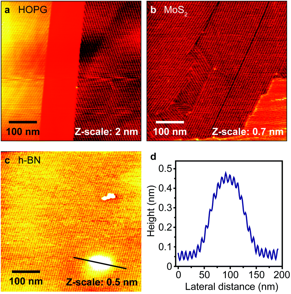 | ||
| Fig. 1 (a–c) AFM topography of the diacetylene molecular layer on HOPG, MoS2 and h-BN, respectively. (d) Spatial profile indicated by the line in (c). | ||
On sapphire, Fig. 2a illustrates the AFM topography over a 4 × 4 μm2 area immediately after the dropcasting. Several islands of diacetylene cover large areas of the surface. The height of most islands vs. the surroundings is 5.5 ± 1.0 nm, indicating that the layer count in those aggregates is the same. As the length of the diacetylene molecule is estimated to be about 3.7 nm, and given the island homogeneity, these results indicate that the molecules are standing up and form bilayers on the substrate as illustrated in Fig. 2b. Note that even though the islands are clearly composed of two molecular layers, it was often possible to identify the layer orientation in detailed AFM scans (Fig. S10 in the ESI†). This is in agreement with the literature,19 where standing up molecules stacked next to each other formed similar patterns. Since the sapphire surface is hydrophilic, the hydrophilic COOH moiety of the molecule interacts preferably with the substrate and not with the hydrophobic alkyl chain moiety. This is the reason why the standing-up configuration is more stable on sapphire than the flat-lying.
 | ||
| Fig. 2 (a and c) AFM topography of annealed sapphire with dropcast diacetylene immediately after the deposition and 24 h after it, respectively. (b and d) Schematic models of the molecular assembly on (a) and (c), respectively. | ||
The inter-island space appears mostly unaffected as confirmed by CM scans performed with high contact force (Fig. S11a, ESI†). The debris spread by the tip within the scanned area is most likely ambient contamination with only a small number of adsorbed molecules. Island formation with relatively clean interspace indicates the attractive molecule–molecule interaction.
Fig. 2c shows the sample topography 24 h after dropcasting. The smaller islands merged into larger aggregates whose height vs. the substrate is again homogeneous, but doubled to 11.1 ± 1.0 nm. This is equivalent to 4 standing-up molecular layers, as illustrated in Fig. 2d. The rest of the surface seems to be clean with the sapphire terraces, the steps of which do not seem to influence the molecular assembly, clearly resolvable. Note that further incubation (up to 72 h) did not lead to higher aggregations (6, 8, 10 layers, etc.). We can assume that the amount of stable molecular layers is analogous to the solution concentration (higher concentration-more layers). The molecular deposition on sapphire clearly leads to a Volmer–Weber (island) growth.
After sapphire, oxidized diamond (bandgap typically 5.5 eV31) was used for the deposition of PDA-precursors. Fig. 3a displays the AFM topography of a 4 × 4 μm2 area on the O-MCD substrate immediately after dropcasting the diacetylene solution. Similar to sapphire, islands of diacetylene are formed on the surface. However, this time the islands are μm-sized immediately after the deposition. In addition, they are stable as their shape and size do not change with time. The islands have sharp edges, indicating that after the first layer is assembled on the surface, the subsequent molecules adhere while preserving the orientation. The height of those islands is 7.9 ± 1.0 nm, while there are few areas 13.1 ± 1.0 nm above the surface, as noted in the image. Those values give a ratio of 3:5 which corresponds to 3 or 5 standing up molecular layers. This configuration is illustrated in Fig. 3b. The inter-island space seems to be clean, similar to sapphire, confirming the attractive molecule–molecule interactions. Growth of diacetylene on O-MCD is therefore also Volmer–Weber.
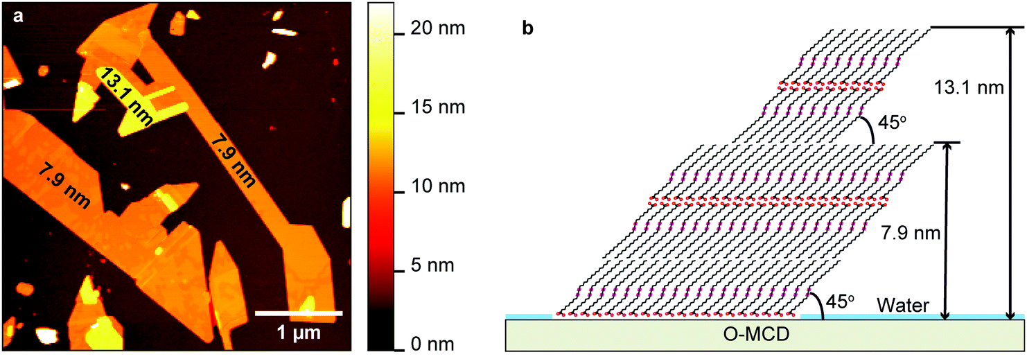 | ||
| Fig. 3 (a) AFM topography of highly polished oxidized single crystal diamond after dropcasting of diacetylene. (b) Schematic model of the molecular assembly. | ||
Sapphire and O-MCD surfaces are hydrophilic and the molecular layers are standing up on them in a similar fashion. However, the stability and the height of the respective molecular islands are different and can be attributed to the higher electronegativity of C vs. Al32 (O has higher electronegativity from both of them). Even though both surfaces are hydrophilic, the Al–O surface dipole exhibits a higher negative charge on the O as compared with the C–O dipole.33 This results in a weaker interaction of the COOH moiety with the O-MCD surface when compared to the sapphire, also corroborated by the cleaner surface after a CM scan (Fig. S11b, ESI†). Another notable difference between the two systems is the even (sapphire) and odd (O-MCD) number of stacked layers. This means that the top side of the layer is hydrophilic COOH on sapphire and hydrophobic CH3 on O-MCD, which suggests that, on the former, the molecular layer is covered in water. This difference is also attributed to the stronger Al–O surface dipole which attracts a larger amount of water on sapphire (compared to O-MCD), as illustrated in Fig. 2b and d.
Regarding the height and the orientation of molecular layers, we assume them to be the same per substrate (e.g. height of top and bottom bilayers on sapphire is the same). Nevertheless, the measured layer height is slightly different between substrates: in the case of sapphire, a monolayer is 2.8 ± 0.2 nm high (11.1 nm:4), while on O-MCD this value is 2.6 ± 0.2 nm (13.1 nm:5). This indicates that the angle of the molecule with respect to the substrate is approximately 49° ± 4° on the former and 45° ± 4° on the latter. The above is corroborated by the AFM height measurements showing nearly identical monolayer height values per substrate on (1) sapphire, where the top and bottom bilayers are both ∼5.5 nm high and (2) O-MCD when comparing the bottom 3-layer with the top 2-layer (7.9 nm and 5.2 nm, respectively).
In order to confirm the surface dipole influence on the molecular assembly, the same MCD sample was cleaned with organics and the diacetylene deposition was repeated after surface hydrogenation. The C–H surface dipole has positive charge on the H (due to the lower electronegativity of H vs. C) and the surface is hydrophobic (contact angle measurements on MCD and sapphire can be seen in the ESI,† Fig. S14). Fig. 4a (AFM topography, 600 × 600 nm2) shows diacetylene aggregates assembled on H-MCD after dropcasting. There is no trend concerning the molecular aggregate height (typically around 40 nm), unlike on sapphire and O-MCD. Fig. S12a in the ESI† shows a detailed AFM topography image (200 × 200 nm2) on top of a molecular aggregate. In the corresponding spatial profile (Fig. S12b, ESI†) we see a 0.3 nm height step between adjacent layers, which corresponds to the distance between two flat-lying molecular layers.34,35 This clearly indicates that the diacetylene molecules are not standing up but the molecular axis is parallel to the substrate surface. On the hydrophobic H-MCD surface, the alkyl chain moiety of the molecule should interact with the surface stronger than the COOH moiety. Therefore, the molecules adsorb on H-MCD in a flat-lying manner.
 | ||
| Fig. 4 (a) AFM topography on hydrogenated polished single crystal diamond after dropcasting of diacetylene. (b) AFM topography on the same area as (a), after scanning in contact mode the area indicated by the square in (a). | ||
The inter-aggregate area exhibits flatness comparable to that of the substrate and seems mostly free of diacetylene molecules at first glance. However, a 200 × 200 nm2 CM scan performed in the area (indicated by the square in Fig. 4a) revealed what was possibly a surface fully covered by several molecular layers after being disrupted by the AFM tip. We can see the surface after the CM scan in Fig. 4b. It is clearly visible that the CM scan induced a large morphology change in the surface, without affecting the surrounding aggregates. This suggests that the molecules that were moved around by the AFM tip immediately merged to form new aggregates. Thus the inter-aggregate area has a layered structure as well (molecules are flat-lying but the layer count is unknown). This is corroborated by the corresponding phase shift image (Fig. S13c, ESI†) which appears homogeneously colored. From Fig. 4a, b and Fig. S13c (ESI†) it is clear that the growth of diacetylene molecules on H-MCD is Stranski–Krastanov (layer-island), as we can identify both several diacetylene islands of varying height (aggregates) as well as homogeneous layers over larger areas (inter-aggregate space). Note that the molecular structure on H-MCD may be related to the crystalline structure of diacetylene molecules in the bulk phase, which is potentially another indication of strong molecule–molecule interactions. Additional discussion on molecular stacking can be read in the ESI.† All molecular layer data on sapphire and MCD are summarized in Table 1.
| Material | Molecular orientation | Layering | Layer height | Monolayer height | Monolayer angle |
|---|---|---|---|---|---|
| Sapphire | Standing | 2–4 | 5.5–11.1 ± 1 nm | 2.8 ± 0.2 nm | 49° ± 4° |
| O-MCD | Standing | 3–5 | 7.9–13.1 ± 1 nm | 2.6 ± 0.2 nm | 45° ± 4° |
| H-MCD | Flat-lying | Hundreds | Tens of nm | 0.3 nm | 0° |
Another way to control the hydrophilicity of a surface is by screening the long-range electrostatic interactions at its liquid–surface interface. It was recently demonstrated that only 20% of those long-range interactions are passing through a monolayer of graphene.36 As presented in the optical micrograph in Fig. 5a a graphene layer was mechanically exfoliated on the ultra-flat sapphire surface before introducing the diacetylene. Fig. 5b depicts AFM topography (500 × 500 nm2) of diacetylene chains self-assembled on the graphene-on-sapphire system. The planar self-assembly appears now similar to the one observed on HOPG, providing a flat-lying SAM albeit with smaller domains than on HOPG. Graphene adhesion on the sapphire substrate is good as evidenced by the two distinct sapphire terraces that can be seen through the graphene in the AFM topography. The result in Fig. 5 indicates that even though we cannot use sapphire directly for the deposition of the diacetylene molecules, it is an excellent atomically flat candidate for graphene support. The graphene screening effect is ensuring the planar self-assembly of diacetylene in air. As graphene can be rendered insulating, while preserving its flatness,37 with nm precision by functionalizing it with a moderated He-ion beam,38 this system can be readily used for on-surface synthesis of single PDA molecular wires and subsequent PDA transport measurements.
 | ||
| Fig. 5 (a) Optical micrograph (120 × 80 μm2) of a graphene flake deposited on an ultra-flat sapphire surface. (b) AFM topography (500 × 500 nm2) showing diacetylene chains lying flat on the graphene. The sapphire terraces roughly dividing the image into halves indicate good adhesion of the graphene on the substrate. | ||
Conclusions
Different substrates were tested to investigate the formation of flat-lying 10,12-nonacosadiynoic acid SAM on a flat insulating surface. The surface of h-BN is appropriate as it provides a SAM similar to HOPG and MoS2, mostly due to its hydrophobic, inert nature and its hexagonal crystal structure. Surface electrostatics (hydrophilicity/hydrophobicity) are essential for the diacetylene arrangement on sapphire, O-MCD and H-MCD. We have demonstrated that sapphire and single crystal diamond are not suitable for self-assembling a flat-lying SAM, as the diacetylene molecules are forming multi-layered aggregates on those substrates. Nevertheless, the polar effect of surfaces like sapphire can be screened by the adsorption of a graphene sheet on which it is possible to form a flat-lying SAM, suitable for on-surface synthesis. The choice between SiO2/h-BN and graphene-on-sapphire for molecular electronic device fabrication depends on the ability to nanofabricate atomically precise electronic contacts on those surfaces with minimal or no contamination introduced to the system.Acknowledgements
We would like to thank Dr M. Osada and Dr S. Nakaharai (NIMS) for important discussions. This work was supported by the World Premier International Research Center Initiative (WPI) and the Ministry of Education, Culture, Sports, Science and Technology of Japan (MEXT), and partially supported by JSPS KAKENHI Grant Numbers 24241047 and 16H03829.References
- N. V. Fischer, U. Mitra, K.-G. Warnick, V. Dremov, M. Stocker, T. Wölfle, W. Hieringer, F. W. Heinemann, N. Burzlaff, A. Görling and P. Müller, Chem. – Eur. J., 2014, 20, 11863–11869 CrossRef CAS PubMed.
- J. Terao, Polym. Chem., 2011, 2, 2444–2452 RSC.
- J. Liu and R. Yang, Phys. Rev. B: Condens. Matter Mater. Phys., 2012, 86, 104307 CrossRef.
- A. Imamura and Y. Aoki, Int. J. Quantum Chem., 2006, 106, 1924–1933 CrossRef CAS.
- Y. Okawa, M. Akai-Kasaya, Y. Kuwahara, S. K. Mandal and M. Aono, Nanoscale, 2012, 4, 3013–3028 RSC.
- T. A. Su, H. Li, M. L. Steigerwald, L. Venkataraman and C. Nuckolls, Nat. Chem., 2015, 7, 215–220 CrossRef CAS PubMed.
- H. Song, M. A. Reed and T. Lee, Adv. Mater., 2011, 23, 1583–1608 CrossRef CAS PubMed.
- G. de Ruiter and M. E. van der Boom, J. Mater. Chem., 2011, 21, 17575–17581 RSC.
- N. Fuentes, A. Martín-Lasanta, L. Álvarez de Cienfuegos, M. Ribagorda, A. Parra and J. M. Cuerva, Nanoscale, 2011, 3, 4003–4014 RSC.
- L. Sun, L. Y. A. Diaz-Fernandez, T. A. Gschneidtner, F. Westerlund, S. Lara-Avila and K. Moth-Poulsen, Chem. Soc. Rev., 2014, 43, 7378–7411 RSC.
- C. Nacci, F. Ample, D. Bleger, S. Hecht, C. Joachim and L. Grill, Nat. Commun., 2015, 6, 7397 CrossRef PubMed.
- Y. Okawa and M. Aono, Nature, 2001, 409, 683–684 CrossRef CAS PubMed.
- A. Miura, S. De Feyter, M. M. S. Abdel-Mottaleb, A. Gesquiere, P. C. M. Grim, G. Moessner, M. Sieffert, M. Klapper, K. Mullen and F. C. De Schryver, Langmuir, 2003, 19, 6474–6482 CrossRef CAS.
- R. Giridharagopal and K. F. Kelly, ACS Nano, 2008, 2, 1571–1580 CrossRef CAS PubMed.
- D. Takajo, A. Inaba and K. Sudoh, Langmuir, 2014, 30, 2738–2744 CrossRef CAS PubMed.
- S. P. Sullivan, A. Schnieders, S. K. Mbugua and T. P. Beebe, Langmuir, 2005, 21, 1322–1327 CrossRef CAS PubMed.
- O. Endo, T. Furuta, H. Ozaki, M. Sonoyama and Y. Mazaki, J. Phys. Chem. B, 2006, 110, 13100–13106 CrossRef CAS PubMed.
- J. P. Rabe, S. Buchholz and L. Askadskaya, Synth. Met., 1993, 54, 339–349 CrossRef CAS.
- K. Takami, J. Mizuno, M. Akai-Kasaya, A. Saito, M. Aono and Y. Kuwahara, J. Phys. Chem. B, 2004, 108, 16353–16356 CrossRef CAS.
- D. W. Britt, U. G. Hofmann, D. Moebius and S. W. Hell, Langmuir, 2001, 17, 3757–3765 CrossRef CAS.
- F. Li, E. Shishkin, M. A. Mastro, J. K. Hite, C. R. Eddy Jr, J. H. Edgar and T. Ito, Langmuir, 2010, 26, 10725–10730 CrossRef CAS PubMed.
- T. Taniguchi and K. Watanabe, J. Cryst. Growth, 2007, 303, 525–529 CrossRef CAS.
- N. Kostoglou, K. Polychronopoulou and C. Rebholza, Vacuum, 2015, 112, 42–45 CrossRef CAS.
- K. G. Saw, J. Mater. Sci., 2004, 39, 2911–2914 CrossRef CAS.
- J. W. Liu, M. Y. Liao, M. Imura, H. Oosato, E. Watanabe, A. Tanaka, H. Iwai and Y. Koide, J. Appl. Phys., 2013, 114, 084108 CrossRef.
- B. Rezek, L. Michalíková, E. Ukraintsev, A. Kromka and M. Kalbacova, Sensors, 2009, 9, 3549–3562 CrossRef CAS PubMed.
- H. Kawarada, Surf. Sci. Rep., 1996, 26, 205–259 CrossRef CAS.
- F. Maier, M. Riedel, B. Mantel, J. Ristein and L. Ley, Phys. Rev. Lett., 2000, 85, 3472–3475 CrossRef CAS PubMed.
- R. Xu, D. He, Y. Zhang, B. Wu, F. Liu, L. Meng, J.-F. Liu, Q. Wu, Y. Shi, J. Wang, J.-C. Nie, X. Wang and L. He, Phys. Rev. B: Condens. Matter Mater. Phys., 2014, 90, 224106 CrossRef.
- M. V. Makarova, Y. Okawa, E. Verveniotis, K. Watanabe, T. Taniguchi, C. Joachim and M. Aono, Nanotechnology, 2016, 27, 395303 CrossRef PubMed.
- E. Verveniotis, J. Čermák, A. Kromka, M. Ledinský and B. Rezek, Nanoscale Res. Lett., 2011, 6, 144 CrossRef PubMed.
- A. L. Allred, J. Inorg. Nucl. Chem., 1961, 17, 215–221 CrossRef CAS.
- M. Yokoyama and T. Ito, Appl. Surf. Sci., 2000, 161–163, 457–463 CrossRef.
- P. Nirmalraj, D. Thompson, A. Molina-Ontoria, M. Sousa, N. Martín, B. Gotsmann and H. Riel, Nat. Mater., 2014, 13, 947–953 CrossRef CAS PubMed.
- A. D. Enevoldsen, F. Y. Hansen, A. Diama, L. Criswell and H. Taub, J. Chem. Phys., 2007, 126, 104703 CrossRef CAS PubMed.
- T. Ondarcuhu, V. Thomas, M. Nunez, E. Dujardin, A. Rahman, C. T. Black and A. Checco, Sci. Rep., 2016, 6, 24237 CrossRef CAS PubMed.
- Y. Naitou, T. Iijima and S. Ogawa, Appl. Phys. Lett., 2015, 106, 033103 CrossRef.
- S. Nakaharai, T. Iijima, S. Ogawa, S. SuzukI, S.-L. Li, K. Tsukagoshi, S. Sato and N. Yokoyama, ACS Nano, 2013, 7, 5694–5700 CrossRef CAS PubMed.
Footnote |
| † Electronic supplementary information (ESI) available: XPS experimental details and spectra, I/V characteristics of diamond, droplet contact angle measurements, supplementary AFM data and secondary discussion on molecular stacking. See DOI: 10.1039/c6cp06749b |
| This journal is © the Owner Societies 2016 |