
 Open Access Article
 This Open Access Article is licensed under a Creative Commons Attribution-Non Commercial 3.0 Unported Licence
Understanding charge transport in non-doped pristine and surface passivated hematite (Fe2O3) nanorods under front and backside illumination in the context of light induced water splitting†
Prince Saurabh
Bassi
a,
Li
Xianglin
b,
Yanan
Fang
b,
Joachim Say Chye
Loo
a,
James
Barber
*ac and
Lydia Helena
Wong
*a
aSchool of Materials Science and Engineering, Nanyang Technological University, Singapore 639798, Singapore. E-mail: lydiawong@ntu.edu.sg
bEnergy Research Institute @ NTU, Nanyang Technological University, 50 Nanyang Drive, Research Techno Plaza, X-Frontier Block, Level 5, Singapore, 637553, Singapore
cDepartment of Life Sciences, Imperial College London, London, SW7 2AZ, UK. E-mail: j.barber@imperial.ac.uk
First published on 10th October 2016
Abstract
Hematite (Fe2O3) nanorods on FTO substrates have been proven to be promising photoanodes for solar fuel production but only with high temperature thermal activation which allows diffusion of tin (Sn) ions from FTO, eventually enhancing their conductivity. Hence, there is a trade-off between the conductivity of Fe2O3, and the degradation of FTO occurring at high annealing temperatures (>750 °C). Here, we present a comprehensive study on undoped Fe2O3 nanorods under front and back illumination to find the optimum annealing temperature. Bulk/surface charge transport efficiency analysis demonstrates minimum bulk recombination indicating overall high quality crystalline Fe2O3 and the preservation of FTO conductivity. Surface recombination is further improved by growing a TiOx overlayer, which improves the photocurrent density from 0.2 mA cm−2 (backside) to 1.2 mA cm−2 under front side and 0.8 mA cm−2 under backside illumination. It is evident from this study that the performance of undoped and unpassivated hematite nanorods is limited by electron transport, whereas that of doped/passivated hematite nanorods is limited by hole transport.
Introduction
It is hoped that the growing global energy demands can be met by solar fuel production arising from novel technological advancements. Hematite, as a photoanode, has been used profoundly with different strategies to improve its performance in PEC devices.1–4 Apart from techniques like doping, surface treatment, integration with a co-catalyst or a heterojunction, one of the fundamentally employed strategies is thermal activation of hematite (Fe2O3) photoanodes via high temperature annealing that yields a significant increase in photocurrent density.5–12 It has been shown by Ling et al. that such annealing of hematite films on FTO substrates allows diffusion of tin (Sn) from the latter into the semiconductor bulk, thus influencing its electrical properties.13 Hence, there is a correlation between photocurrent and the Sn concentration in hematite, whereby the photocurrent increase is due to an increase in electrical conductivity with higher Sn4+ ion diffusion. Morrish et al. reported that activation of hematite nanorods could be achieved using a longer annealing process at a relatively lower temperature.7 High temperature annealing affects the substrate texture and reduces the electrical conductivity of FTO substrates. Hence, for a long and sustainable use, it is advisable to use comparatively lower annealing temperatures for constructing hematite photoanodes in PECs to avoid FTO deformation while allowing for thermal activation of hematite.Here, pristine Fe2O3 nanorods synthesized through a hydrothermal technique and annealed for different profiles have been reported. Photoelectrochemical characterization of these pristine films under front side and backside illumination was investigated to understand how charge transfer affects PEC performance. Pristine nanorods were then coated with a TiOx overlayer using Atomic Layer Deposition (ALD) to reduce surface recombination and improve charge transfer to the electrolyte. Characterization of photocurrent transients, electrochemical impedance spectroscopic analysis and bulk/surface charge transport efficiency evaluation were also performed to gain an insight into the charge transport in pristine and coated films. This, to the best of our knowledge, is the first report of the PEC characterization of undoped pristine and surface passivated hematite nanorods using front side and backside illumination supported by Electrochemical Impedance Spectroscopy (EIS) and measurement of bulk/surface charge transport efficiency.
Results and discussion
Pristine Fe2O3 nanorods with different annealing profiles were fabricated as mentioned in Section S1, ESI.† Structural/morphological characterization and photoelectrochemical characterization under front and backside illumination were performed for pristine hematite nanorods (details in Sections S2 and S3, ESI†). Similar processes for fabrication and characterization were also followed for ALD grown TiOx coated thin films. The schematic representation for all fabrication processes is shown in Fig. S1 (ESI†). The charge transport for different sides of illumination i.e. backside and front side is illustrated in Fig. 1(a). Front side illumination is when light falls on the semiconductor side resulting in charge generation near the semiconductor/electrolyte interface, whereas backside illumination is when light is directed from the FTO side and hence the photon absorption takes place near the FTO/semiconductor junction.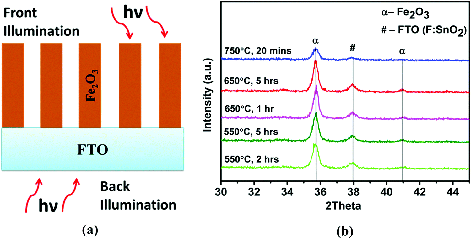 | ||
| Fig. 1 (a) Schematic representation of hematite nanorods under front and back side illumination; (b) XRD spectra of pristine hematite nanorods prepared with different annealing profiles. | ||
The XRD patterns of all the samples are presented in Fig. 1(b). The peaks corresponding to a 2theta value of 35.7° were considered for the Gaussian fit. The peak intensity and FWHM values for different samples were: [550 °C, 2 h]: (200, 0.43), [550 °C, 5 h]: (219, 0.40), [650 °C, 1 h]: (235, 0.39), [650 °C, 5 h]: (245, 0.38) and [750 °C, 20 min]: (89, 0.43). The peak intensity increases with annealing temperature up to 650 °C but decreases significantly at 750 °C probably due to deformation of FTO, as reported by Annamalai et al.14 The FWHM was minimum and the intensity was maximum for 650 °C, 5 h, and crystallinity was the highest for these samples as compared to other samples. To compare samples diverse in their crystallinity and doping profile; only 550 °C, 2 h, 650 °C, 5 h and 750 °C, 20 min samples were compared and studied in detail. Photoelectrochemical characterization under front side and backside illumination of the other two samples was also performed as shown in Fig. S2 (ESI†). It shows that the performance for 550 °C, 5 h is identically low (<0.1 mA cm−2) in the range from onset potential 0 V vs. Ag/AgCl (1 V vs. RHE) to dark current onset i.e. around 0.5 V vs. Ag/AgCl (1.5 V vs. RHE) as for 550 °C, 2 h. In the same potential range, the photocurrent density for 650 °C, 1 h was lower than 650 °C, 5 h samples under back illumination.
After hydrothermal processing, FeOOH nanorods were formed as reported previously15 (the cross-section image is shown in Fig. S3, ESI†), with a square cross-section, sharp edges and average rod length of around 700 nm. After annealing with different profiles as mentioned above, these yellow-colored nanorods changed to orange red-colored films indicating the change of phase to α-Fe2O3 (shown in Fig. S1 (ESI†)). The FESEM images of these hematite films (as shown in Fig. S4, ESI†) confirmed the circular cross-section of Fe2O3 nanorods with a diameter of around 70 nm for 550 °C, 2 h films. With higher annealing temperatures, the diameter of nanorods increased to about 100 nm probably due to the aggregation of nanorods in agreement with an earlier report by Ling et al.13 Energy Dispersive X-ray Spectra (EDS) were obtained for 650 °C, 5 h and 750 °C, 20 min annealed films (shown in Fig. S5, ESI†) which confirmed the presence of Sn in the latter only, due to the Sn diffused from FTO.
J–V plots for pristine hematite nanorods prepared with different annealing temperatures are shown in Fig. 2(a). The measurements were performed under backside and front side illuminations for all samples, the schematic of which is shown in Fig. 1(a). It was observed that the sample annealed at 550 °C, 2 h yielded very low photocurrent density for both front side and backside illumination, indicating that carrier generation and their separation were limited because of the poor charge transport properties of crystalline hematite.13 In general, the samples showed improved photocurrent density when the annealing temperature increased to 650 °C and 750 °C for both front side and backside illuminations. This can be attributed to the effect of improved crystallinity and Sn diffusion from FTO leading to doping of Sn4+ ions into the hematite semiconducting layer,13 which induces additional charge carriers (i.e. electrons) in hematite nanorods. The absorption spectra of pristine nanorods under backside and front side illumination are shown in Fig. 2(b). It is observed that the absorption decreased with increasing annealing temperature because of the agglomeration of nanorods, leading to a smaller surface area and, hence, a lesser light trapping capability. For all films, samples with front side illumination showed a higher apparent absorption as compared to the backside illumination. It is probably due to the higher reflectance by the intervening FTO layer for the backside illuminated sample, as observed from the diffuse reflectance shown in Fig. S6 (ESI†).
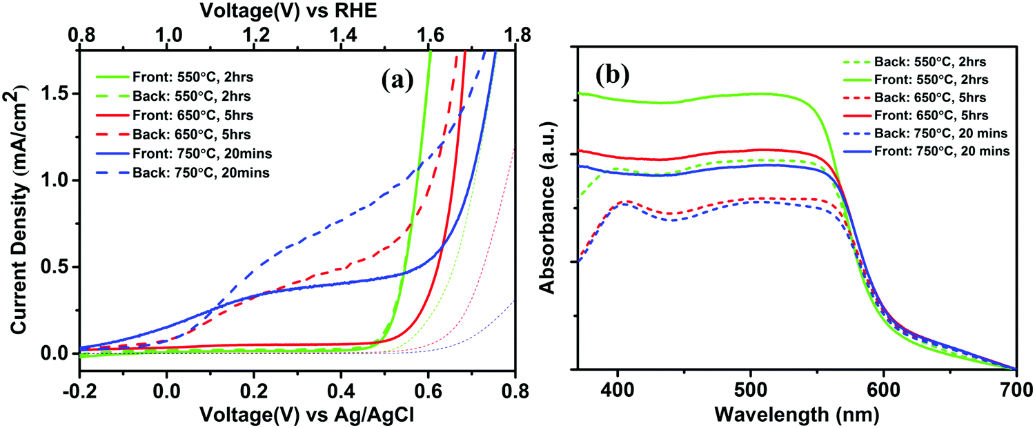 | ||
| Fig. 2 (a) Photocurrent density–potential (J–V) plots and, (b) absorption spectra for hematite nanorods fabricated using different annealing temperatures under back and front illumination. | ||
To further investigate the trends the photocurrent density–potential plots show, Incident Photon to Current Efficiency (IPCE) spectra were evaluated for all the samples as shown in Fig. 3(a). With increasing annealing temperature, the IPCE increased as in the case of photocurrent density due to increasing conductivity and crystallinity. Under backside and front side illumination for respective samples, the plots exhibited a similar trend to the photocurrent density. The IPCE for front side illumination for all samples was lower than for backside which was is in contrast to the absorption spectra as shown in Fig. 2(b), where the front side absorption for all the samples was higher than the backside absorption. Hence, even though there are less photons being absorbed, backside illumination yields higher photocurrent and IPCE than front side illumination, which is hypothesized to be due to the better charge transport driven by fast electron extraction to the back contact. This shows that the reason behind photocurrent density trends is not the change in absorption but the charge dynamics of the system.
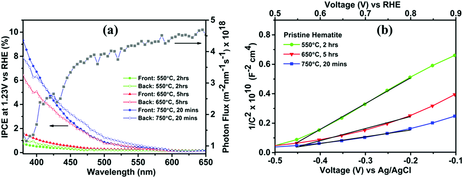 | ||
| Fig. 3 (a) IPCE spectra for hematite films fabricated with varied annealing temperatures under back and front side illumination. Grey curve represents solar photon flux with varying wavelength, (b) Mott Schottky plots for pristine Fe2O3 nanorods prepared with different annealing profiles. | ||
Mott Schottky analysis was performed for these films, as shown in Fig. 3(b), which yielded a trend of decreasing slope of curves with increasing annealing temperature. As mentioned in Section S3 (ESI†), donor density increased with the decreasing slope. Hence, with higher annealing temperature, the donor density increased, probably due to an increase in the Sn diffusion from FTO into the bulk semiconductor layer. This would explain the general trend in the photocurrent density and the IPCE spectra. It must be noted that since Mott Schottky plots yield more accurate values of donor density for compact thin films with the determined geometric area, the MS plots for Fe2O3 nanorods were only utilized to observe a comparative trend in donor density as opposed to the absolute values.
The trends of J–V and IPCE curves could be explained using the schematic representation of pristine nanorods under front and backside illumination, as shown in Fig. 4. The orange colored region represents the absorption depth of around 120 nm for lowest energy photons (∼550 nm) with the total nanorods length of 700 nm (represented as the red region). For the case of front side illumination, electrons have to travel a longer distance to FTO as compared to backside illumination where the accumulation of charge is higher due to the close proximity of photogenerated electrons with the FTO back contact. Since the electrons are the majority carriers in an n-type semiconductor photoanode, their movement is driven by the conductivity of charge carriers in the bulk. This conductivity depends largely on carrier concentration, since hematite possesses a low electron mobility of around 10−2 cm−2 V−1 s−1. This can be improved by adding electronic dopants to assist n-type doping.1 On the other hand, the minority carriers (i.e. holes) could move under electrical drift if they were generated in the depletion region or by diffusion if generated outside the space charge layer. Due to the low minority carrier diffusion length in hematite (2–4 nm),1 transporting these holes into the electrolyte before undergoing recombination is the key to obtaining a good efficiency. Space charge regions in nanorods are formed along the edges, arising from which hole transport occurs radially outwards from their edges (semiconductor/electrolyte interface) into the electrolyte. Since it is known that undoped and un-passivated hematite nanorods exhibit poor surface properties and slow water oxidation kinetics, the holes are trapped and accumulated at the semiconductor/electrolyte interface in both front side and backside illumination. Hence, electron transport becomes the limiting factor for photocurrent density, which defines the photocurrent in undoped/un-passivated hematite.
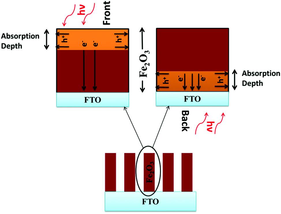 | ||
| Fig. 4 Schematic representation of electron/hole transport in hematite nanorods under front and backside illumination. | ||
For 550 °C hematite, the conductivity in the bulk is very poor resulting in slow electron transport and hence in low photocurrent for both front side and backside illumination, as shown in Fig. 2(a). Interestingly, for 650 °C hematite, the front side photocurrent is minimal due to poor electron transfer to the back contact but under backside illumination, the electron collection at the back contact is higher and hence shows significant photocurrent density. This trend for back- and front side photocurrent values is also similar to the hematite annealed at 750 °C. Backside photocurrent is relatively higher than front side photocurrent due to the proximity of photogenerated electrons to the back contact. For the 750 °C samples, the electron transport to the back contact is easier compared to front side illumination because of the increased conductivity from doping of Sn4+ ions in the bulk. Hence, the photocurrent density under front side illumination was higher for 750 °C as compared to that for 650 °C samples. Another observation from Fig. 2(a) is the difference between the onset potential for the 750 °C annealed samples under front and backside illumination. The holes are generated in the proximity of the semiconductor–electrolyte interface under front side illumination as opposed to backside illumination. This allows easier transfer of holes under built-in field to the electrolyte and hence lower onset potential. All these interpretations confirm an earlier report by Liang et al. which showed that the limiting factor in undoped Fe2O3 is the electron transport whereas for the Sn-doped Fe2O3, it is hole transport.16
It has been shown through spectral evidence that photocurrent increased with increasing applied bias. This is due to decreasing electron density in the bulk which inhibits back electron–hole recombination in the semiconductor layer.17,18 This is in compliance with the photocurrent trend observed for the samples, where apparently the back electron–hole recombination mechanism is being suppressed through efficient collection of electrons at the back contact when using backside illumination.
To investigate whether shorter nanorods will affect the trend in the photocurrent density, samples deposited under conditions of 100 °C, 4 h and 100 °C, 2 h were also characterized as shown in Fig. S7, ESI.† The trend of backside illumination being more effective than the front side illumination agreed with the samples annealed at 650 °C, 5 h; whereas the trend was reversed for 100 °C, 2 h samples annealed at 750 °C, 20 min i.e. the front side photocurrent surpassed the backside photocurrent, which could possibly be due to the increased electron conductivity that drives photocurrent under front side illumination. Since holes are generated near the semiconductor–electrolyte interface, the holes are easily injected into the electrolyte and electrons easily traverse to the back contact, implying higher photocurrent under front side illumination.
To gain an insight into hole accumulation at the semiconductor/electrolyte interface, the photocurrent density was evaluated under chopped light for both front and backside illumination as shown in Fig. 5. The anodic transient for front side illumination was observed to be smaller than the backside illumination. This could be due to photogenerated holes being produced closer to the semiconductor/electrolyte surface and hence the hole accumulation on the surface is low. However, under backside illumination, holes accumulate on densely concentrated nanorods near FTO and hence the recombination of holes with photogenerated electrons is much higher than in the case of front side illumination.
 | ||
| Fig. 5 J–V plot for hematite thin films fabricated with different annealing temperatures under (a) backside and (b) front side illumination of chopped solar simulated light. | ||
As discussed earlier, the charge transport in the pristine films under different annealing conditions was limited to electron transport to the back contact. Hence, to explore the charge dynamics of the bulk, Electrochemical Impedance Spectroscopy (EIS) was performed for all the samples under front side and backside illumination and under dark conditions at 1.23 V vs. RHE. The Nyquist plots for these measurements are shown in Fig. 6 below. The equivalent circuit fitted along with its variables is shown in Fig. 6(b). Rs is the series resistance which depends on the contact of the external circuit with FTO, Cbulk is the capacitance of the bulk semiconducting layer, Rtrap is the resistance of the trapping of both photogenerated charge carriers at the surface states, Rct,ss is the resistance to transfer of holes to the electrolyte through those surface states and Css is the capacitance attributed to the surface states. This circuit helps to discuss the role played by surface states on hematite nanorods.
 | ||
| Fig. 6 Nyquist plots for pristine hematite thin films under (a) back and (b) front side illumination (inset: Nyquist plot for films under dark conditions for comparison). | ||
Under dark conditions, the RCT values were very high, being of the order of 6 MΩ for all the films. This is expected due to the absence of minority carriers (as shown in the inset of Fig. 6(a)). Under both backside and front side illumination, Rtrap and Rct,ss decreased with higher temperature annealing and were the lowest for the 750 °C samples, which implies that holes from the valence band were more likely to inject into the electrolyte through surface states rather than undergoing bulk recombination with electrons. This symbolizes the importance of Sn4+ ion diffusion from FTO which increased the electron transport in bulk by increasing the carrier concentration and hence conductivity.
For the 650 °C samples, Rtrap under front side illumination was high at 14 KΩ whereas under backside illumination it was 1.4 KΩ. This denotes increased conductivity and hence low bulk recombination. This trend was similar to that of the 750 °C samples, implying that the electron transport under backside illumination was higher than the front side illumination, which followed the earlier trends shown by photocurrent density and IPCE spectra. Rct,ss under backside illumination was lower as compared to front side illumination for all annealing profiles. This could be due to lower surface recombination of holes with photogenerated electrons at the semiconductor–electrolyte interface in the case of backside illumination where electron extraction to the back contact is efficient.
To account for the bulk and surface charge transfer efficiency for the above samples, photoelectrochemical characterization in the presence of a hole scavenger, H2O2, in the electrolyte, was performed. The use of the hole scavenger allows the fast injection of holes into the electrolyte and hence the surface charge transfer efficiency, denoted η(catalysis), with H2O2 becomes unity.19 Further details about the measurement are discussed in Section S3, ESI† while the J–V plots for all samples with 1 M NaOH + 0.5 M H2O2 as the electrolyte are shown in Fig. 7(a) below. For all the samples, the backside photocurrent (JH2O2) was higher than the front side photocurrent probably due to better electron collection in the backside while the hole transport for both sides is efficient owing to the hole scavenging properties of H2O2. The difference between front and back was small for the 750 °C annealed samples, which is due to better electron transport even for the front side owing to higher conductivity of the sample as compared to the case for other two samples. Fig. 7(b) shows the bulk [η(separation)] and surface [η(catalysis)] charge separation efficiencies for these samples in the voltage region occurring before their dark current onset. The bulk charge separation efficiency for backside illumination is higher for all the samples presumably due to higher electron transport. This efficiency for 650 °C is higher than doped samples (750 °C) in spite of Jabs of 750 °C being higher which motivated us to work at this temperature to effectively tackle the problem of bulk recombination.
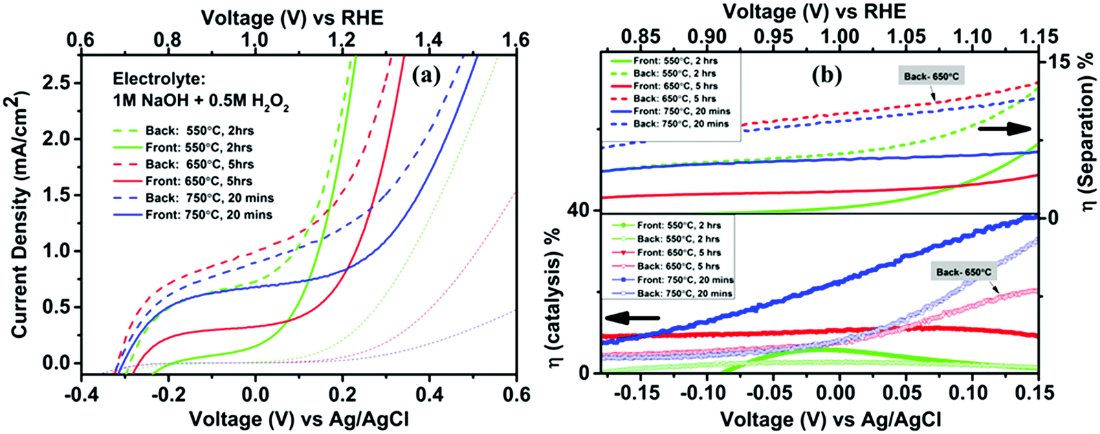 | ||
| Fig. 7 (a) J–V plots and (b) bulk/surface charge transport efficiency curves for all the samples measured under back and front side illumination in the presence of hole scavenger H2O2. | ||
While the 650 °C samples achieved the highest bulk charge separation efficiency, the 750 °C sample had the highest surface charge transfer efficiency under both front and backside illuminations. This suggested that the surface properties of 750 °C samples were much better than the 650 °C samples. Hence, to improve the surface kinetics of the 650 °C samples, for which surface recombination was the limiting factor, surface passivation of hematite nanorods was performed and the results discussed in the following section.
Surface passivation of Fe2O3 nanorods using an ALD grown TiOx overlayer
As the η(separation) was the highest for 650 °C samples, this means that bulk recombination was minimum under backside illumination. For the 650 °C samples, the challenge was to increase the surface charge transfer efficiency, represented as η(catalysis), which reflects on the surface recombination of photogenerated holes with surface defects or traps present on the semiconductor/electrolyte interface. Many surface passivation strategies have been used with hematite and other types of photoanodes, such as CoF3,20 Al2O3,21 Ga2O3,22 SnO215 and ZnO.23 These additions to the semiconductor surfaces have been effective in enhancing hole injection into the electrolyte by passivating surface defects or changing hole transfer kinetics resulting in a cathodic shift in the onset potential and enhancing the photocurrent density. Recently, TiOx coated Fe2O3 nanorods have been reported by Li et al.24 which yielded enhanced performance as compared to pristine nanorods. Here, we employed a TiOx overlayer using the Atomic Layer Deposition (ALD) technique to understand its role in charge transport under both front side and backside illuminations.The ALD technique allows a precise control of a thin overlayer with similar geometry to the base material, in this case, nanorods. Tetrakis(di methyl amido)titanium (TDMATi) and H2O precursors were alternately pulsed onto the FeOOH nanorods under the conditions mentioned in Section S1 (ESI†). This resulted in a very thin overlayer of TiOx, of around 5 nm. Due to high temperature annealing at 650 °C for 5 h, Fe atoms diffused into the overlayer and Ti atoms diffused inwards which resulted in a very thin overlayer of FexTiyOz (∼8 nm) on the top of Fe2O3.24 The methodology for ALD coated hematite nanorods from the earlier reports by Li et al.24 was followed and the in-detail morphological characterization was obtained by FESEM. The images obtained for the coated thin films (shown in Fig. S8, ESI†) showed no significant difference in the dimensions from the pristine nanorods. For both samples, nanorods of around 700 nm in length and a circular cross-section of diameter around 80–100 nm were observed. A High Resolution Transmission Electron Microscopic (HRTEM) image of a crystalline Fe2O3 nanorod and a contrasting overlayer of FexTiyOz (thickness around 8 nm) on top of nanorods is as shown in Fig. S9 (ESI†). From the interplanar spacing, d = 0.44 nm, it is evident that the conformal layer could be Fe2TiO5 with the (210) lattice plane. The presence of Ti is also corroborated through the EDS spectra as shown in Fig. S9(c) (ESI†). Since the phase of the overlayer is crucial for the further understanding of this system, it should be investigated through other specific characterization tools.
Photoelectrochemical characterization was performed to observe the effect of TiOx coating on the photocurrent density under front and backside illumination as shown in Fig. 8. After coating with the TiOx overlayer, the photoanode under front side illumination yielded a higher photocurrent of 1.2 mA cm−2vs. 0.8 mA cm−2 for backside at 1.23 V vs. RHE. This is opposite to the trend observed in the pristine sample and shows the effectiveness of surface passivation in enhancing the hole injection into the electrolyte. The IPCE spectra of coated and pristine thin films are shown in Fig. 8(b). It shows the IPCE of coated films around 35% and 22% for 380 nm photons under front side and backside illumination, respectively. This is a significant improvement compared with pristine nanorods that exhibit IPCE values of around 5% and 2% for backside and front side illumination respectively for 380 nm photons. This trend is consistent with the photocurrent trends shown earlier. For coated films, the front side IPCE was higher than the backside IPCE, consistent with the photocurrent density, which could be due to the higher absorption exhibited by the former (Fig. 9(a)). For pristine nanorods, the backside IPCE is higher because the electron transport, which is the driving force for photocurrent under poor hole injection into the electrolyte, is the controlling factor. For coated films, higher absorption in the front side yields higher IPCE probably due to the better hole injection into the electrolyte after surface passivation.
 | ||
| Fig. 8 (a) Standard J–V plots and (b) IPCE spectra for pristine and TiOx coated hematite films under back and front side illumination. | ||
 | ||
| Fig. 9 (a) Absorption and (b) J–V plots under chopped light, for pristine and TiOx coated hematite films under front and back side illumination. | ||
The absorption spectra shown in Fig. 9(a) show that the front side absorption is apparently higher for both pristine and coated films as compared to the back illuminated sample. This is, as mentioned earlier for pristine films, probably due to the higher reflectance by the intervening FTO layer for the back side illuminated sample. The effect of surface passivation could be observed in chopped photocurrent density–potential curves shown in Fig. 9(b). Anodic and cathodic transients for coated films diminished as compared to the pristine films, indicating that there is no hole accumulation on the surface, and photogenerated holes and electrons participate efficiently in photocurrent as compared to pristine nanorods.
Charge transport in coated nanorods was investigated by performing photoelectrochemical characterization under the influence of a hole scavenger (H2O2) as shown in Fig. 10(a). The photocurrent density was higher for backside illuminated pristine Fe2O3 nanorods than for the front side with H2O2 in the electrolyte, which is similar to the photocurrent trend without H2O2. On the other hand, the coated nanorods yielded a similar photocurrent under backside and front side illumination. This suggests that after introduction of the hole scavenger, hole injection into the electrolyte no longer limits the photocurrent and, hence, the photons absorbed control the photocurrent. This could be understood by observing the bulk and surface charge transfer efficiency as shown in Fig. 10(b). The bulk charge separation efficiency, η(separation), which determines the amount of bulk recombination of charge carriers, suggests that for coated films, backside efficiency is higher than the front side efficiency which could be due to Jabs which is lower under backside since JH2O2 is similar for both sides. This means that the photogenerated holes are transported to the electrode surface more effectively under backside illumination possibly due to inhibition of the back electron–hole recombination mechanism owing to better electron collection at the back contact. In contrast, the surface charge transfer efficiency is lower for backside suggesting that the hole injection into the electrolyte limits the photocurrent. Another interesting observation is that bulk charge separation efficiency exhibited by both pristine and coated films under backside illumination was similar suggesting that holes reach the surface efficiently. Whereas the limiting factor was the hole injection into the electrolyte due to which the difference in surface charge transfer efficiency, η(catalysis), was observed under backside illumination. After coating with the TiOx overlayer, η(catalysis) increased and reached a level as high as 70% at 1.15 V vs. RHE for front side illumination as compared to very low efficiency, of the order of 10%, displayed by the pristine nanorods. This suggests that the performance of pristine nanorods was limited by hole injection into the electrolyte. This is improved after coating TiOx on top of hematite, which substantiates its role as a surface passivating layer. It is to be noted that the region chosen for the efficiency curve is upper bounded by the dark current onset potential and lower bounded by the region where positive photocurrent is observed.
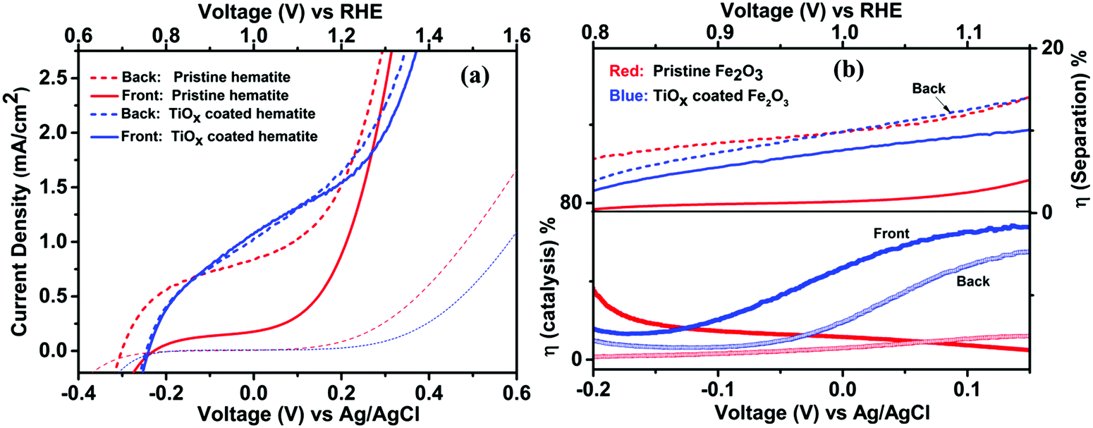 | ||
| Fig. 10 (a) Current–potential curves for pristine and TiOx coated hematite thin films under the presence of hole scavenger (H2O2), and (b) charge carrier efficiency for surface [η(catalysis)] and bulk [η(separation)] for pristine and coated films. | ||
Conclusion
Pristine hematite nanorods were synthesized under different annealing profiles for application as photoanodes in PEC and characterized under front and backside illuminations. Undoped hematite nanorods annealed at 650 °C for 5 h displayed higher photocurrent under backside illumination as compared to the front side due to the better electron transport in the former. Bulk charge separation efficiency was the highest for this system indicating low bulk recombination. This improvement is attributed to good electron extraction to the back contact in thermally activated and crystalline hematite nanorods, while avoiding damage to the morphology or conductivity of the FTO substrates. Hence, this annealing profile of 650 °C, 5 h was used for surface passivation to reduce surface recombination. An ALD grown TiOx overlayer on top of hematite nanorods resulted in an overlayer of Fe2TiO5 (∼8 nm) after a solid state reaction at high temperature. A manifold enhancement in performance was observed after TiOx coating, with the photocurrent reaching around 1.2 mA cm−2 at 1.23 V vs. RHE under front side illumination. It was found that after coating, the front side photocurrent exceeded the backside, which was in contrast to the trend in pristine nanorods where the significant backside photocurrent was mainly driven by electron transport. Through the evaluation of IPCE and charge separation efficiency, it was illustrated that the hole injection into the electrolyte was enhanced due to the overlayer. Moreover, photons absorbed were more efficient in generating photocurrent due to the inhibition of electron–hole recombination.One of the points of observation is that the light penetration is limited due to the absorption depth being smaller than the length of nanorods. Since the hydrothermal reaction includes both nucleation and growth of nanorods on substrates, it is difficult to control the length of nanorods while keeping their density intact. This could be further explored using the Anodic Aluminum Oxide (AAO) template method or by further optimizing the hydrothermal conditions. While light penetration is a limiting factor in performance of nanorods, it is similar for both front and back side illumination. Hence, the final deciding factor is the electron extraction after the photons are absorbed and converted to charge carriers. This investigative study is helpful in the understanding of charge transport in hematite nanorods under front and backside illumination. It also highlights a sequential improvement in their performance through the inhibition of bulk and surface recombination reactions.
References
- K. Sivula, F. Le Formal and M. Grätzel, ChemSusChem, 2011, 4, 432–449 CrossRef CAS PubMed.
- Y. Lin, G. Yuan, S. Sheehan, S. Zhou and D. Wang, Energy Environ. Sci., 2011, 4, 4862–4869 CAS.
- O. Zandi and T. W. Hamann, Phys. Chem. Chem. Phys., 2015, 17, 22485–22503 RSC.
- Y. Lin, G. Yuan, S. Sheehan, S. Zhou and D. Wang, Energy Environ. Sci., 2011, 4, 4862–4869 CAS.
- D. A. Wheeler, G. Wang, Y. Ling, Y. Li and J. Z. Zhang, Energy Environ. Sci., 2012, 5, 6682–6702 CAS.
- P. S. Bassi, Gurudayal, L. H. Wong and J. Barber, Phys. Chem. Chem. Phys., 2014, 16, 11834–11842 RSC.
- R. Morrish, M. Rahman, J. M. D. MacElroy and C. A. Wolden, ChemSusChem, 2011, 4, 474–479 CrossRef CAS PubMed.
- D. Wang, Y. Zhang, C. Peng, J. Wang, Q. Huang, S. Su, L. Wang, W. Huang and C. Fan, Adv. Sci., 2015, 2, 1500005 CrossRef PubMed.
- J. Moir, N. Soheilnia, K. Liao, P. O'Brien, Y. Tian, K. S. Burch and G. A. Ozin, ChemSusChem, 2015, 8, 1557–1567 CrossRef CAS PubMed.
- B. Iandolo, B. Wickman, I. Zoric and A. Hellman, J. Mater. Chem. A, 2015, 3, 16896–16912 CAS.
- T.-Y. Yang, H.-Y. Kang, K. Jin, S. Park, J.-H. Lee, U. Sim, H.-Y. Jeong, Y.-C. Joo and K. T. Nam, J. Mater. Chem. A, 2014, 2, 2297–2305 CAS.
- P. S. Bassi, R. P. Antony, P. P. Boix, Y. Fang, J. Barber and L. H. Wong, Nano Energy, 2016, 22, 310–318 CrossRef CAS.
- Y. Ling, G. Wang, D. A. Wheeler, J. Z. Zhang and Y. Li, Nano Lett., 2011, 11, 2119–2125 CrossRef CAS PubMed.
- A. Annamalai, A. Subramanian, U. Kang, H. Park, S. H. Choi and J. S. Jang, J. Phys. Chem. C, 2015, 119, 3810–3817 CAS.
- L. F. Xi, S. Y. Chiam, W. F. Mak, P. D. Tran, J. Barber, S. C. J. Loo and L. H. Wong, Chem. Sci., 2013, 4, 164–169 RSC.
- Y. Liang, C. S. Enache and R. van de Krol, Int. J. Photoenergy, 2008, 2008, 1–7 CrossRef.
- M. Barroso, S. R. Pendlebury, A. J. Cowan and J. R. Durrant, Chem. Sci., 2013, 4, 2724 RSC.
- F. Le Formal, S. R. Pendlebury, M. Cornuz, S. D. Tilley, M. Gratzel and J. R. Durrant, J. Am. Chem. Soc., 2014, 136, 2564–2574 CrossRef CAS PubMed.
- H. Dotan, K. Sivula, M. Gratzel, A. Rothschild and S. C. Warren, Energy Environ. Sci., 2011, 4, 958–964 CAS.
- Y. S. Hu, A. Kleiman-Shwarsctein, G. D. Stucky and E. W. McFarland, Chem. Commun., 2009, 2652–2654, 10.1039/B901135h.
- F. Le Formal, N. Tétreault, M. Cornuz, T. Moehl, M. Grätzel and K. Sivula, Chem. Sci., 2011, 2, 737–743 RSC.
- T. Hisatomi, F. Le Formal, M. Cornuz, J. Brillet, N. Tetreault, K. Sivula and M. Gratzel, Energy Environ. Sci., 2011, 4, 2512–2515 CAS.
- L. Xi, P. S. Bassi, S. Y. Chiam, W. F. Mak, P. D. Tran, J. Barber, J. S. Chye Loo and L. H. Wong, Nanoscale, 2012, 4, 4430–4433 RSC.
- X. Li, P. S. Bassi, P. Boix, Y. Fang and L. H. Wong, ACS Appl. Mater. Interfaces, 2015, 7, 16960–16966 CAS.
Footnote |
| † Electronic supplementary information (ESI) available. See DOI: 10.1039/c6cp05379c |
| This journal is © the Owner Societies 2016 |