
 Open Access Article
 This Open Access Article is licensed under a Creative Commons Attribution-Non Commercial 3.0 Unported Licence
The butterfly – a well-defined constant-current topography pattern on Si(001):H and Ge(001):H resulting from current-induced defect fluctuations†
Mads
Engelund‡
 *a,
Szymon
Godlewski‡
b,
Marek
Kolmer
b,
Rafał
Zuzak
b,
Bartosz
Such
b,
Thomas
Frederiksen
cd,
Marek
Szymonski
b and
Daniel
Sánchez-Portal
ac
*a,
Szymon
Godlewski‡
b,
Marek
Kolmer
b,
Rafał
Zuzak
b,
Bartosz
Such
b,
Thomas
Frederiksen
cd,
Marek
Szymonski
b and
Daniel
Sánchez-Portal
ac
aCentro de Física de Materiales (CFM), CSIC-UPV/EHU, Paseo Manuel de Lardizabal 5, 20018, Donostia-San Sebastián, Spain. E-mail: mads.engelund@gmail.com
bCentre for Nanometer-Scale Science and Advanced Materials (NANOSAM), Faculty of Physics, Astronomy and Applied Computer Science, Jagiellonian University, Krakow, Poland
cDonostia International Physics Center (DIPC), Paseo Manuel de Lardizabal 4, 20018, Donostia-San Sebastián, Spain
dIKERBASQUE, Basque Foundation for Science, E-48013, Bilbao, Spain
First published on 20th June 2016
Abstract
Dangling bond (DB) arrays on Si(001):H and Ge(001):H surfaces can be patterned with atomic precision and they exhibit complex and rich physics making them interesting from both technological and fundamental perspectives. But their complex behavior often makes scanning tunneling microscopy (STM) images difficult to interpret and simulate. Recently it was shown that low-temperature imaging of unoccupied states of an unpassivated dimer on Ge(001):H results in a symmetric butterfly-like STM pattern, despite the fact that the equilibrium dimer configuration is expected to be a bistable, buckled geometry. Here, based on a thorough characterization of the low-bias switching events on Ge(001):H, we propose a new imaging model featuring a dynamical two-state rate equation. On both Si(001):H and Ge(001):H, this model allows us to reproduce the features of the observed symmetric empty-state images which strongly corroborates the idea that the patterns arise due to fast switching events and provides an insight into the relationship between the tunneling current and switching rates. We envision that our new imaging model can be applied to simulate other bistable systems where fluctuations arise from transiently charged electronic states.
1 Introduction
The continuous miniaturization of electronic devices has directed many fundamental research efforts toward creating atomic-scale circuits.1,2 Scanning tunneling microscopy (STM)3 has become one of the most important tools for nanoscale characterization. It allows not only for nanometer-scale surface analysis, but also for controlled on-surface manipulation of individual atoms and molecules.4–10 The STM technique becomes particularly powerful when applied to the Si(001):H and Ge(001):H substrates, where atomically precise patterns of surface dangling bonds (DBs) can be created.11–21 This patterning process is central to a diverse set of proposals for nanoscale circuitry, either using DB arrays directly as logic-gate components and wires,13,16,18,22–24 or as templates for further processing steps.1,25–28 Surface DBs can also be applied for contacting organic molecules with the substrate.29–31The ability to manipulate DBs, however, comes at a cost. Often images recorded on DB arrays are difficult to interpret because the underlying tunneling processes are complicated and because the DBs interact in a complex way with the scanning tip.32 This is due to the presence of metastable states, which can be switched dynamically during imaging.14,21,32–34 This situation is not unique to DB arrays and other studies have explored microscopy and spectroscopy under similar conditions.35–38
Recently the dynamic behavior of DB dimers (DBD) on Ge(001):H, when empty states are imaged by STM, was reported.15 A DBD can be created by the selective removal of two H atoms from the hydrogenated Ge(001)39 or Si(001)12 surfaces. As shown in Fig. 1A and B, this results in a buckled ground-state geometry with one atom at a higher position over the surface than the other. This configuration is degenerate with the mirror-symmetric situation, i.e., the system is bistable. Despite this geometric asymmetry it was found that empty-state STM imaging of DBDs on Ge(001):H15 and Si(001):H39 results in a symmetric pattern.
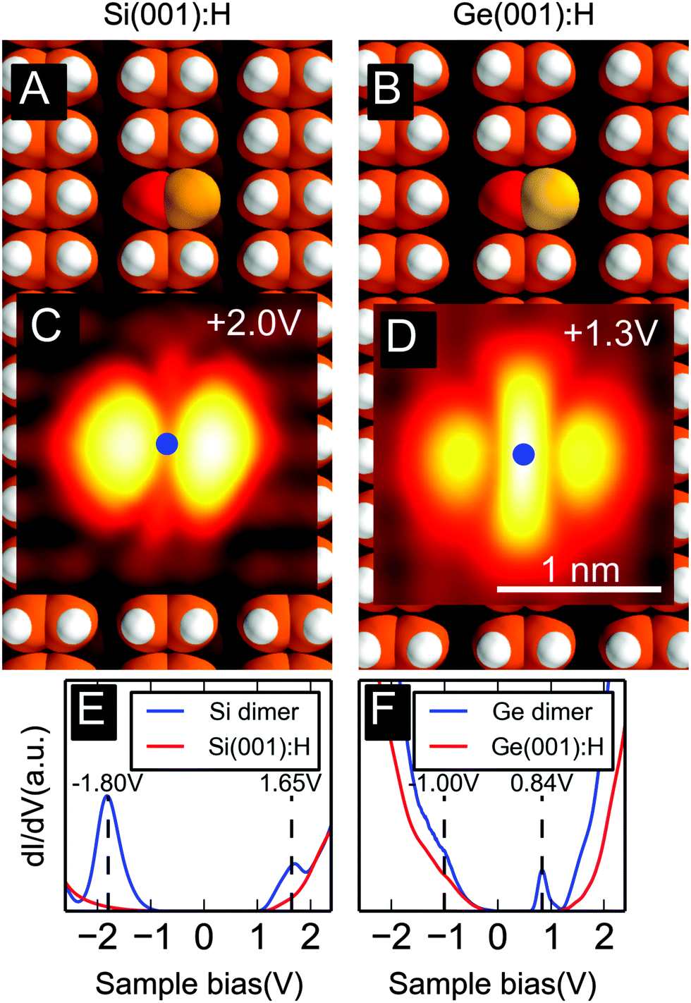 | ||
| Fig. 1 (A and B) Calculated, relaxed geometries of a DBD in the Si(001):H and Ge(001):H substrates, respectively. The large spheres are Si/Ge atoms while the small ones are H atoms. The coloring depends on the height of the atoms (darker nuances towards bulk). (C and D) Experimental empty-state constant-current STM images of a DBD on Si(001):H (I = 10 pA; VS = 2.0 V) and Ge(001):H (I = 20 pA; VS = 1.3 V), respectively. The sample voltage VS was chosen to achieve the strongest signal from to the defect compared to the background. The blue dots mark the lateral position of the STM tip during acquisition of the spectroscopy data. (E and F) Experimental dI/dV spectra of Si(001):H and Ge(001):H, respectively, recorded over the central part of the dimer (blue) and a reference measurement (red) on the passivated substrate revealing features attributed to the DBD defect states (marked with vertical dashed lines). | ||
Such symmetric empty-state DBD images are shown in Fig. 1C and D for two different surfaces. Due to the appearance of three characteristic lobes (two side-lobes and a central lobe separated by sharp dips) we call this pattern “the butterfly”. On Si(001):H the side-lobes are dominant to an extent that the central lobe is only visible slightly off the dimer axis. The situation is reversed for Ge(001):H, where instead the central lobe is dominant. These detailed features have so far eluded a precise explanation, although it has been proposed that rapid oscillations15 or characteristic excited states11 are decisive in the butterfly-like appearance.
On Ge(001):H the behavior is somewhat different for filled-state imaging. Here static, asymmetric features can be observed for sample voltages around VS = −0.5 V while the onset of switching events occurs at VS ∼ −0.7 V.15 In the latter fluctuation regime it is reasonable to expect that integration over a sufficiently long time scale would give rise to symmetric filled-state STM images. Thus, if similar switching also takes place under empty-state imaging conditions, this could be invoked to explain the observed symmetric STM images in Fig. 1C and D. We find that understanding the origin of the butterfly shape of the experimental STM images requires a model that goes beyond a simple average of the contributions from two configurations. The description of this model is the main focus of the present work.
In this paper, we take advantage of the strong and distinctive butterfly pattern to reveal the underlying physics. At sufficiently low sample voltages we are able to resolve in time a bistable switching and characterize how the switching rate grows rapidly with larger voltages. We demonstrate that this low-voltage behavior can be extrapolated to explain the symmetric and feature-rich, empty-state images. The experimental DBD images can be reproduced by solving a rate equation for each and every tip position to find the appropriate time-averaged current over the two ground-state configurations. While previous studies have proposed similar models to compute the current through a tunnel junction,40–42 to the best of our knowledge, this is the first time that such a model has been used to reproduce STM images. Furthermore, our imaging model may have a wider applicability to other bistable systems where fast fluctuations are induced by the transiently charged electronic states that are the intermediates in the overall tunneling processes.
2 Methods
2.1 Experimental details
The experiments were performed using an Omicron low temperature STM operated at liquid helium temperature (5 K) with electrochemically etched tungsten tips used as probes.The nominally undoped Ge(001) samples (TBL Kelpin crystals, n-type, 45 Ωcm) were prepared by several cycles of argon ion sputtering and annealing.39 The passivation by a hydrogen layer was performed by exposure of clean samples to atomic hydrogen obtained from a home built hydrogen cracker.39 Note that although nominally undoped, the finally prepared Ge(001):H samples tend to be significantly p-doped regardless of intrinsic doping – even to the extent that n-doped samples tend to have inversion layers.43
Si(001):H samples were provided by CEA-LETI Grenoble.12 They contained two hydrogen terminated samples prepared in a reduced-pressure chemical vapor deposition (RP-CVD) reactor and bonded together by van der Waals forces. In order to obtain the hydrogen terminated reconstructed surface the 200 nm diameter starting wafers undergo a multistep preparation process including wet chemical cleaning and thermal treatment.12 The Si samples were slightly p-doped with a resistivity of 10.5 Ωcm corresponding to the doping level of 1015 at cm−3. The samples were de-bonded in situ under UHV conditions providing high quality hydrogenated Si(001):H surfaces for atomic scale experiments. The preparation procedure delivers samples that could be characterized by STM at liquid helium temperature (5 K) as demonstrated in our previous studies.12,14,16
The dI/dV data were obtained by averaging of several I(V) curves followed by a numerical differentiation. The switching rates were determined from I(t) traces exhibiting a two-level character registered for various tunneling current and bias voltage settings. For STM image processing the SPIP and WSxM44 software packages were applied.
2.2 Calculation details
Geometric relaxations were performed using spin-polarized density-functional theory using the SIESTA code.45 Our model systems, shown in Fig. 1A and B, consisted of a 3 × 6 surface supercell with 7 Si/Ge layers, including the Si/Ge(001):H reconstruction, and a passivating di-hydride layer on the reverse side of the slab where the Si/Ge atoms keep their bulk positions. We used a double-ζ plus polarization basis set with orbital radii defined using a 100 meV energy shift,45 the Perdew–Burke–Ernzerhof (PBE) version of the generalized gradient approximation for exchange–correlation,46 a real-space grid equivalent to a 300 Ry plane-wave cutoff, and a 2 × 3 × 1 k-point grid for Brillouin zone sampling (a higher sampling density parallel to the dimer rows is chosen to account for the typically larger dispersion of the surface electronic features along this direction). On the reverse side of the slab the two last Si/Ge layers and the hydrogen passivation layer were kept fixed, while all other atoms were relaxed until forces were smaller than 0.02 eV per Å. Calculations of charged systems were performed using a uniform compensating background charge. Potential energy landscapes were calculated by constraining the difference in height between the two atoms comprising the DBD, while relaxing all other degrees of freedom.To compute the STM images an accurate description of the decay into vacuum of the defect state wave-function, and in particular its nodal planes, proved crucial.47,48 Therefore, we followed the surface integration technique of Paz and Soler.49 When the total electron density falls below 0.0001 Å−3, all wavefunctions, ψn, are propagated into the vacuum assuming a constant exponential decay, κn. Here κn was determined using the energy eigenvalue en relative to the vacuum level, 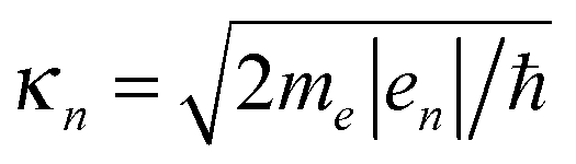 . We used the Tersoff–Hamann approximation50 in our simulations. In this method the current is assumed to be proportional to the local density of states (LDOS) evaluated in the center of curvature of the tip. Since the constant-current experimental images in Fig. 1C and D are acquired using different current values for Si and Ge, we think that a consistent and convincing theory–experiment comparison requires the use of the same proportionality constant a in order to relate the LDOS and the current for both substrates. We chose a = 0.01 Å3A for this ratio. With this value of a, which was determined by inspection, we can get a good agreement between theoretical and experimental STM images for both substrates. However, it is worth noting that the value of a is not critical and can be changed in a relatively wide range. Finally, in order to mimic the effect of the tip in reducing the resolution of the STM images, we have convoluted our currents with a Gaussian kernel K(r,r′) = (πσ2)−3/2e−|r−r′|2/2σ2 with σ = 0.5 Å.
3 Results & discussion
As explained above, the characteristic butterfly pattern occurs in empty-state imaging of DBDs on both Si(001):H and Ge(001):H surfaces as shown in Fig. 1C and D. In Fig. 1E we show dI/dV spectra recorded over the center of the dimer on Si(001):H. It reveals well-defined peaks around −1.80 V and 1.65 V. Note that the positions of the observed resonances cannot be directly linked with the energies of the relevant DBD states due to the band bending effects resulting in an upward shift of empty state resonances and a downward movement of filled state ones. Similarly, as shown in Fig. 1F, a shoulder and a peak structure are observed on Ge(001):H around −1.00 V and 0.84 V, respectively. We attribute the peaks to localized gap states of the dimer and the shoulder to a similar state below the valence band edge of Ge(001):H. The existence of such states is corroborated by our density-functional calculations.The calculated unoccupied gap states are shown in Fig. 2A and B for the Si(001):H and Ge(001):H surfaces along with the corresponding calculated constant-current STM topographies in Fig. 2C and D. Evidently, these unoccupied gap states are asymmetric with respect to the surface rows and therefore cannot alone explain the symmetric butterfly pattern observed in the experiments. Additionally, we observe that these gap states are rather similar for both surfaces – the main difference is a stronger asymmetry for Ge than Si, which is seen most clearly in the calculated STM topographies. This difference probably arises from the fact that the Ge DBD has a larger charge-polarization than its Si counterpart, which in turn causes the unoccupied electronic states to have a greater weight over the positively charged (lower) site and moves the nodal plane in the opposite direction towards the negatively charged (upper) site. For Ge the electronic asymmetry overcompensates for the geometric one and the lower site appears brighter for empty-state imaging. Curiously, for Si the geometric and electronic asymmetry compensate each other to a large extent. We will see later that the degree of asymmetry plays a crucial role in the appearance of the final STM image.
 | ||
| Fig. 2 (A and B) Isosurfaces of the computed unoccupied gap state wave function superimposed on the structural model of the DBD on Si(001):H and Ge(001):H, respectively. The two different colors of the isosurface represent opposite signs of the isovalue (±0.003 Å−3/2). (C and D) Calculated local density of states (LDOS) isosurface of the unoccupied gap state (color scale range is 1.5 Å; iso-LDOS value is 10−10 Å−3). Within the Tersoff–Hamann approximation,50 this can be regarded as a constant-current STM image. The unoccupied DBD gap state can be loosely described as an anti-bonding combination of a p-orbital on the lower site and an sp3 hybridized orbital on the upper site. | ||
3.1 Observation of dimer switching on Ge(001):H
We next turn to the observations of rapid switching of the DBDs at low temperatures. To investigate this, we analyze the low-bias telegraph noise for fixed tip positions recorded on dimers in Ge(001):H.As recently shown by Wojtaszek et al.,43 STM measurements can be performed at very small sample voltages VS on the Ge(001):H substrate, even with only several tens of mV applied, both in the empty- and filled-state imaging modes. This is in marked contrast to the Si(001):H substrate, where the larger band gap hinders measurements for VS between approximately −1 V and +1 V. For VS = ±1 V, the recorded images on Si(001):H are perfectly stable and smooth (no fluctuations can be resolved). At these voltages the switching rates of the DBD are likely to exceed the apparatus time resolution. A detailed analysis of DBD switching behavior is therefore limited to Ge(001):H.
The disparity between the two substrates is likely connected to the substantially smaller gap of Ge. For negative bias voltages the different energetic position of the occupied DBD state with respect to the bulk states probably also plays an important role. As can be seen in Fig. 1E and F, the occupied DBD state on Ge(001):H is well below the edge of the valence band, in contrast to that of Si(001):H. Any hole created by tip extraction of an electron is therefore expected to have a longer lifetime in the Si-DBD state than in the Ge-DBD resonance, which increases the efficiency of energy transfer to vibrations and consequently the switching rate.
In Fig. 3A we show how the STM image of a Ge-DBD evolves from being stable at low negative voltage into being increasingly dominated by discrete jumps, which create the streaky image at VS = −1 V. The bistable character of the jumps resulting in a two-level telegraph noise of the current I versus time t traces is shown in Fig. 3B. By characterizing the frequency of these jumps presented in Fig. 3C and D we observe that the DBD switching on Ge(001):H can be recorded over a large current and voltage range for negative VS. The dependence of the switching rate on voltage (Fig. 3C) shows that the switching starts around VS = −0.6 V, which is where the tail of the filled-state resonance begins. The switching rate then grows quickly at larger voltages, indicating that the switching is efficiently initiated when electrons are extracted from the DBD state.
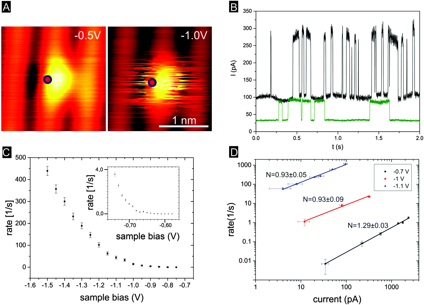 | ||
| Fig. 3 Experimental observation of DBD switching on Ge(001):H at negative sample voltages VS. (A) Filled-state STM images showing a static, buckled DBD imaged at VS = −0.5 V (left) and a streaky pattern originating from DBD switching at VS = −1.0 V (right). (B) Current I versus time t traces recorded for two different vertical tip heights resulting in comparatively large (black curve, lower tip altitude) and small (green trace, higher tip altitude) tunneling currents. Both traces were acquired with VS = −1.0 V. (C) Dependence of the switching rate on VS recorded with a tunneling current of I = 100 pA (I = 780 pA in the inset). (D) Dependence of the switching rate versus I recorded at different VS. Circles in panel A mark the position of the STM tip during the recording of the current traces and thus for the determination of the switching rate. | ||
In Fig. 3D we analyze further the switching rate as a function of the tunnel current I (in the low current state), and find it to be proportional to IN with an exponent N ∼ 1, indicating that DBD switching is essentially a one-electron process. For the smaller voltage, i.e., VS = −0.7 V, close to the threshold voltage, the rate increases slightly faster than being linear with the exponent reaching N = 1.29. This may suggest that here also two-electron processes play a role.35
Now we turn our attention to the switching rates in the positive low-bias regime on Ge(001):H. Due to experimental difficulties in this regime, the recorded maximal switching rate and the tunneling current are substantially lower than those of negative voltages. The positive low-voltage measurements proved difficult, since these measurements are performed within the surface band gap.51 In order to maintain the desired tunneling current within the band gap the feedback loop has to approach the tip close to the substrate. A further increase of the tunneling current leads to the unstable behavior due to the significant reduction of the tip altitude, close approach to the surface and increased interaction between the tip apex and surface atoms.
Typical STM images showing switching events are displayed in Fig. 4A for three different bias voltages. As demonstrated in the inset in Fig. 4B, in this regime the dimer on Ge(001):H switches between asymmetric states at a rate roughly proportional to the STM current, which provides an indication that the positive-bias switching is dominated by one-electron processes.
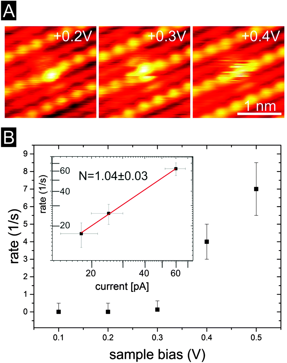 | ||
| Fig. 4 (A) Experimental empty-state images of DBD switching on Ge(001):H at different positive sample voltages VS > 0 (I = 10 pA). (B) Dependence of the switching rate on VS for fixed I = 10 pA as well as on I for fixed VS = +0.45 V (inset). | ||
The effective excitation of frequent switching for Ge(001):H is demonstrated in Fig. 4B, where the switching rate starts growing rapidly beyond a voltage of VS ∼ 0.3 V. The switching rate exceeds the time resolution limit of the apparatus already at VS = 0.7 V leading to completely smooth symmetric STM images of the defect at higher voltages15 as shown in Fig. 1C (see also ESI,† Fig. S2 for further details). It is worth noting that at higher temperatures thermal excitations may also lead to switching of the DBD between the two configurations. However, as discussed in more detail in the ESI,† thermal fluctuations would give rise to STM images characterized by a different symmetric pattern than that discussed here. This gives additional support to the current-induced switching mechanism presented here.
3.2 Energetic barriers and the origin of the switching events
In Fig. 5 we show the potential energy landscape for neutral and negatively charged DBDs. Here we plot the total energy as a function of the relative height of the two atoms forming the dimer. In order to obtain these data we constrained the height difference of the dimer atoms while allowing all other degrees of freedom to relax. By examining the DBD in the Frank–Condon regime,52i.e., disregarding electronic and vibrational relaxations, we can evaluate whether a single electron tunneling event can possibly cause a switching event. The data in Fig. 5 indicate that this is indeed the case. After an instantaneous (vertical) electronic transition from neutral to negatively charged, the energy of the system will be higher than the charged-state minimum by ∼0.2 eV and ∼0.3 eV, on Si and Ge, respectively (see the red arrows in Fig. 5). Since those values are substantially higher than the energy barrier for switching in the charged-state on both substrates (∼0.1 eV), we can conclude that switching by a single-electron process is possible. However, a requirement is that electronic and vibrational relaxation times are both at least of the same order-of-magnitude as the time needed to move a substantial length on the potential energy surface of the charged system, which we estimate to be in the order of ∼100 fs.§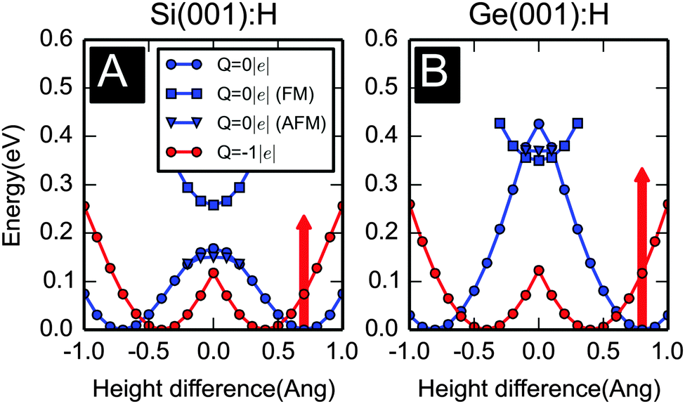 | ||
| Fig. 5 Total energy as a function of the difference in height for the two atoms comprising the DBD for (A) Si and (B) Ge. For the neutral DBD (Q = 0, blue), in addition to the non-spin-polarized solution it was possible to stabilize both ferromagnetic (FM) and anti-ferromagnetic (AFM) spin-polarized solutions when the height of the two dimer sites is similar. For the negatively charged DBD (Q = −1|e|, red) a single state was found. The total energy is given with respect to the lowest energy for each charge state. The vertical arrow represents the energy of a charged DBD evaluated using the neutral-state relaxed geometry (and measured with respect to the fully relaxed charged configuration). | ||
An interesting feature of the data presented in Fig. 5 is the existence of stable spin-polarized solutions for configurations close to the transition state. We find a ferromagnetic (FM) state that exhibits a local minimum in the symmetric atomic configuration, and it is even more stable than the unpolarized and anti-ferromagnetic (AFM) solutions in the case of Ge. Since it has a different overall spin than the ground state DBD, it could be a relatively long-lived state. However, in all our current traces for both positive and negative voltages, we observe only two distinct levels of the current, suggesting that only the two-fold degenerate asymmetric ground states are at play. In other words, additional levels that could be attributed to other charge and/or spin-polarized states were absent on the time-scale of our instrumental resolution of ∼1 ms.
The absence of long-lived charged states in DBDs is consistent with the available experimental information, in marked contrast to the case of single DBs. For single DBs it is typically possible to generate long-lived charged states that cause bright/dark halos in the STM images around the defects depending on the charge state and imaging conditions. These charge related halos have been consistently reported for single DBs,19,21 but are completely absent when imaging DBDs. This clearly indicates the shorter lifetimes of the charged states in DBDs, which are thus well below the instrumental resolution. However, the charge states are likely to play the dominant role in switching (as mentioned above, the only requirement being that their lifetimes should be at least in the order of hundreds of femtoseconds). The observed high switching rate, as well as its linear dependence on the current, strongly indicates that single-electron tunneling events can cause the observed switching. Furthermore, our calculations show that this picture is fully consistent with the energetics of the system.
To go beyond the above estimates and actually calculate the switching rates is a highly nontrivial task, particularly in the described physical regime, as it would involve an accurate calculation of both electronic and vibrational lifetimes. The electronic lifetimes are expected to be highly dependent on the tip-induced field and therefore on the precise doping conditions of the substrate as well as on the imaging voltage. Rather than embarking on this task, we seek a way to model the STM images without the need for explicitly computing the switching rates.
3.3 Modeling the butterfly-like image
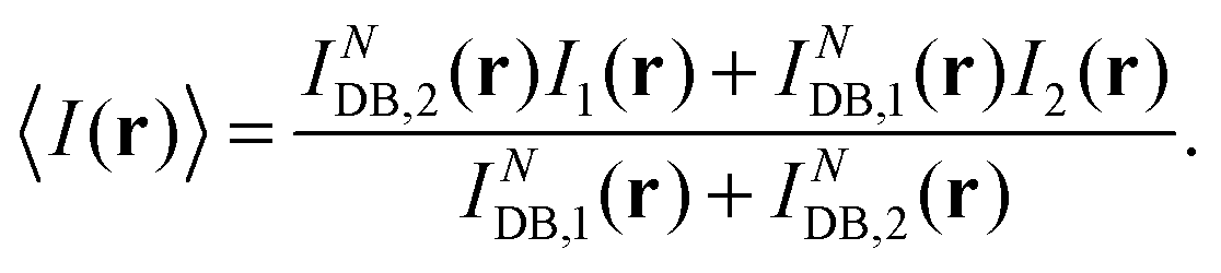
Based on our experimental observations that (i) no long-lived charged or excited states of the DBD are observed, (ii) imaging involves DBD defect states inside the semiconductor band gap, and (iii) current-driven fluctuations occur between the two equivalent DBD tilted configurations, we propose the simple assumption that the switching rate depends exclusively on the current through the electronic resonances of the neutral asymmetric dimer. For positive voltages the relevant current would be the injection into the unoccupied gap state.This assumption leads to the following simple two-level model, similar to earlier works explaining dI/dV spectra.40–42 For each tip position r the time-averaged current 〈I〉 is expressed in terms of the state occupations n1(2)(r) and the corresponding instantaneous currents I1(2)(r),
| 〈I(r)〉 = n1(r)I1(r) + n2(r)I2(r), | (1) |
| ṅ1(r) = n2(r)Γ2→1(r) − n1(r)Γ1→2(r), | (2) |
| ṅ2(r) = n1(r)Γ1→2(r) − n2(r)Γ2→1(r), | (3) |
| Γ1→2(r) = αINDB,1(r), | (4) |
| Γ2→1(r) = αINDB,2(r), | (5) |
The model leads to the following simple expression for the time-averaged current,
 | (6) |
Another observation, which has important consequences for the appearance of the STM image, is that if the DB current dominates the total current and if the current for a given (off-center) tip position is much larger than the other, i.e., I1,2 ≈ IDB,1,2 and IDB,1 ≪ IDB,2, then 〈I(r)〉 ≈ IDB,1[1 + (IDB,1/IDB,2)N−1], e.g., for N = 1, one has 〈I(r)〉 ≈ 2IDB,1. Thus, the time-averaged current is dominated by the low-current configuration for each tip position for N > 0. This observation explains the presence of the pronounced nodal features which, assuming a simple linear average (N = 0), would disappear (see ESI† Section 1 for further details).
Since we cannot access the switching rate at the bias voltage of VS = 1.3 V, at which the butterfly pattern is observed, we extrapolate the linear behavior observed at low positive voltages (see Fig. 4) and also assume N = 1 for higher voltages. This extrapolation is questionable, since higher-order processes could contribute at higher voltages. However, the most important features of the topography only have a very low sensitivity to the value of N ≥ 1 (see ESI† Section 2 for further details). The consequence of this low sensitivity is that (1) our reproduction of the main image features does not depend on the actual value of N, but also conversely that (2) we cannot determine N based on the features of the constant-current topography.
Our procedure for simulating the experimental empty-state constant-current images thus amounts to the following steps: (i) we compute the instantaneous tunneling currents IDB,1(2)(ri) and IO,1(2)(ri) with the dimer in each of the two configurations on a 3D grid of tip positions {ri}. Note that with the help of the Tersoff–Hamann approximation,50 this only amounts to computing the LDOS at {ri}. (ii) For each tip position ri we evaluate the corresponding time-averaged current 〈I(ri)〉 according to eqn (6). (iii) Constant-current topographies are determined from interpolation.
In Fig. 6, we directly compare the simulated STM images with the experimental ones, and as one can see, the dominant features are well reproduced. From our model we see that it is the nodal plane of the empty-state wave function which gives rise to the two symmetric crescent-shaped depressions separating the three lobes in the image. Each dip corresponds to the nodal plane position in one of the two asymmetric geometries. We note that, using the method by Paz and Soler,49 the appearance of the simulated STM images is only weakly dependent on the details of the calculations. It is possible to obtain results similar to those presented in Fig. 6 using less stringent computational parameters. We have explictly checked this using slabs containing only 4 bulk layers, the Γ-point only for k-sampling, a single-ζ-polarized basis set, 150 Ry mesh cutoff, and 150 meV energy shift to fix the orbital radii.
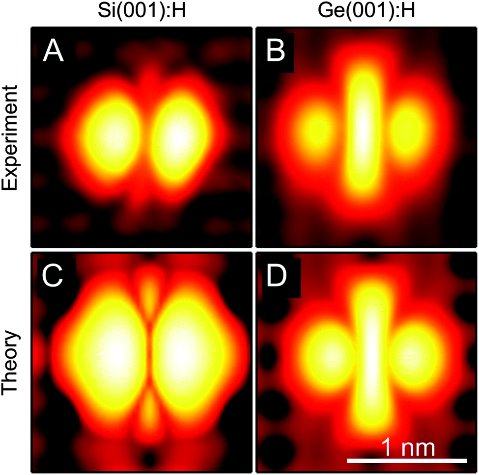 | ||
| Fig. 6 (A and B) Experimental constant-current empty-state images of DBDs on Si(001):H (I = 10 pA; VS = 2.0 V) and Ge(001):H (I = 20 pA; VS = 1.3 V), respectively (same data as in Fig. 1). (C and D) The corresponding simulated STM images using the two-level fluctuation model described according to eqn (6). The range of the color scale, which is the same for theory and experiment, corresponds to 3.5 Å and 2.0 Å for Si and Ge, respectively. | ||
The central lobe arises due to the asymmetry of the unoccupied DBD state. Since the node of the wavefunction is off-centered compared to the dimer row both the asymmetric positions will give a large current in the center of the dimer. For a weakly asymmetric wave function (Fig. 2A), which occurs in Si, the nodal planes of the two configurations essentially coincide and the central lobe almost vanishes. On the other hand, for a strongly asymmetric wave function (Fig. 2B), which occurs in Ge, the nodal planes are spatially separated and the central lobe becomes broader and more dominant.
In addition to the features of the butterfly motif we can also reproduce the transition as the voltage sweeps the resonance (see ESI† Section 4).
4 Conclusions
The very distinctive butterfly-like, empty-state image observed using a STM provides an excellent test-bed for the general understanding of DB arrays. Based on the extensive recording of telegraph noise for DBD switching on Ge(001):H we have proposed a model to theoretically simulate the time averaged images over fast current-induced switching events. This model avoids explicitly calculating the switching rates, but is still able to qualitatively reproduce the features of the experimental STM images as well as the observed differences between the Si(001):H and Ge(001):H substrates. We have demonstrated that rapid fluctuations between several configurations can result in well-defined and distinct patterns rather than a simple smearing of the image features.Our model can be applied to low-temperature STM imaging of other systems dominated by current-induced fluctuations between equivalent states arising from a single type of electronic transition, e.g., the silicon quantum dots investigated by Yamazaki et al.38 or the hydrogen transfer reactions studied by Kumagai et al.35 It should be noted that this model cannot be directly applied to well-separated DBs due the existence of non-equivalent long-lived (charged) states. We consider the extension of the model to encompass this regime as a topic of future work. We hope that this work will inspire further efforts to simulate STM images taking into account dynamical effects.
Acknowledgements
The authors thank Dr Jorge Iribas Cerda and Dr Jakub Lis for helpful discussions. The work was funded by the European Commission under the FP7 FET-ICT “Planar Atomic and Molecular Scale devices” (PAMS) project (Contract No. 610446) and National Science Centre, Poland (2014/15/D/ST3/02975). ME, TF, and DSP also acknowledge support from the Spanish Ministerio de Economía y Competitividad (MINECO) (Grant No. MAT2013-46593-C6-2-P) and the Basque Dep. de Educación and the UPV/EHU (Grant No. IT-756-13). MK acknowledges financial support received from the Foundation for Polish Science (FNP). RZ acknowledges support received from KNOW (scholarship KNOW/44/SS/RZ/2015). Visualizations were performed using Matplotlib,53 MayaVi54 and Origin.55 The publication fee was provided by the CSIC Open Access Publication Support Initiative.References
- M. Fuechsle, J. A. Miwa, S. Mahapatra, H. Ryu, S. Lee, O. Warschkow, L. C. L. Hollenberg, G. Klimeck and M. Y. Simmons, Nat. Nanotechnol., 2012, 7, 242–246 CrossRef CAS PubMed.
- J. S. Prauzner-Bechcicki, S. Godlewski and M. Szymonski, Phys. Status Solidi A, 2012, 209, 603–613 CrossRef CAS.
- G. Binning, H. Rohrer, C. Gerber and E. Weibel, Phys. Rev. Lett., 1982, 49, 57 CrossRef CAS.
- D. M. Eigler and E. K. Schweizer, Nature, 1990, 344, 524–526 CrossRef CAS.
- D. M. Eigler, C. P. Lutz and W. E. Rudge, Nature, 1991, 352, 600–603 CrossRef CAS.
- L. Grill, K.-H. Rieder, F. Moresco, S. Stojkovic, A. Gourdon and C. Joachim, Nano Lett., 2005, 5, 859–863 CrossRef CAS PubMed.
- S.-W. Hla, L. Bartels, G. Meyer and K.-H. Rieder, Phys. Rev. Lett., 2000, 85, 2777–2780 CrossRef CAS PubMed.
- S.-W. Hla, J. Vac. Sci. Technol., B: Microelectron. Nanometer Struct. – Process., Meas., Phenom., 2005, 23, 1351 CrossRef CAS.
- F. Rosei, M. Schunack, P. Jiang, A. Gourdon, E. Laegsgaard, I. Stensgaard, C. Joachim and F. Besenbacher, Science, 2002, 296, 328–331 CrossRef CAS PubMed.
- I. Swart, T. Sonnleitner, J. Niedenführ and J. Repp, Nano Lett., 2012, 12, 1070–1074 CrossRef CAS PubMed.
- S. R. Schofield, P. Studer, C. F. Hirjibehedin, N. J. Curson, G. Aeppli and D. R. Bowler, Nat. Commun., 2013, 4, 1649 CrossRef CAS PubMed.
- M. Kolmer, S. Godlewski, R. Zuzak, M. Wojtaszek, C. Rauer, A. Thuaire, J. M. Hartmann, H. Moriceau, C. Joachim and M. Szymonski, Appl. Surf. Sci., 2014, 288, 83–89 CrossRef CAS.
- R. A. Wolkow, L. Livadaru, J. Pitters, M. Taucer, P. Piva, M. Salomons, M. Cloutier and B. V. C. Martins, in Field-Coupled Nanocomputing, ed. N. G. Anderson and S. Bhanja, Springer, Berlin Heidelberg, 2014, ch. 3, vol. 8280, pp. 33–58 Search PubMed.
- M. Engelund, R. Zuzak, S. Godlewski, M. Kolmer, T. Frederiksen, A. García-Lekue, D. Sánchez-Portal and M. Szymonski, Sci. Rep., 2015, 5, 14496 CrossRef CAS PubMed.
- S. Godlewski, M. Kolmer, J. Lis, R. Zuzak, B. Such, W. Gren, M. Szymonski and L. Kantorovich, Phys. Rev. B: Condens. Matter Mater. Phys., 2015, 92, 115403 CrossRef.
- M. Kolmer, R. Zuzak, G. Dridi, S. Godlewski, C. Joachim and M. Szymonski, Nanoscale, 2015, 7, 12325–12330 RSC.
- H. Labidi, M. Taucer, M. Rashidi, M. Koleini, L. Livadaru, J. Pitters, M. Cloutier, M. Salomons and R. A. Wolkow, New J. Phys., 2015, 17, 073023 CrossRef.
- J. L. Pitters, I. A. Dogel and R. A. Wolkow, ACS Nano, 2011, 5, 1984–1989 CrossRef CAS PubMed.
- M. Taucer, L. Livadaru, P. G. Piva, R. Achal, H. Labidi, J. L. Pitters and R. A. Wolkow, Phys. Rev. Lett., 2014, 112, 256801 CrossRef PubMed.
- A. Bellec, D. Riedel, G. Dujardin, O. Boudrioua, L. Chaput, L. Stauffer and P. Sonnet, Phys. Rev. Lett., 2010, 105, 048302 CrossRef CAS PubMed.
- A. Bellec, L. Chaput, G. Dujardin, D. Riedel, L. Stauffer and P. Sonnet, Phys. Rev. B: Condens. Matter Mater. Phys., 2013, 88, 241406(R) CrossRef.
- H. Kawai, F. Ample, Q. Wang, Y. K. Yeo, M. Saeys and C. Joachim, J. Phys.: Condens. Matter, 2012, 24, 095011 CrossRef PubMed.
- A. Kleshchonok, R. Gutierrez and G. Cuniberti, Nanoscale, 2015, 7, 13967–13973 RSC.
- A. Kleshchonok, R. Gutierrez, C. Joachim and G. Cuniberti, Sci. Rep., 2015, 5, 14136 CrossRef CAS PubMed.
- P. G. Piva, G. a. DiLabio, J. L. Pitters, J. Zikovsky, M. Rezeq, S. Dogel, W. A. Hofer and R. A. Wolkow, Nature, 2005, 435, 658–661 CrossRef CAS PubMed.
- B. Weber, S. Mahapatra, H. Ryu, S. Lee, A. Fuhrer, T. C. G. Reusch, D. L. Thompson, W. C. T. Lee, G. Klimeck, L. C. L. Hollenberg and M. Y. Simmons, Science, 2012, 335, 64–67 CrossRef CAS PubMed.
- A. Fuhrer, M. Füchsle, T. C. G. Reusch, B. Weber and M. Y. Simmons, Nano Lett., 2009, 9, 707–710 CrossRef CAS PubMed.
- G. Scappucci, G. Capellini, W. M. Klesse and M. Y. Simmons, Nanoscale, 2013, 5, 2600–2615 RSC.
- S. Godlewski, M. Kolmer, H. Kawai, B. Such, R. Zuzak, M. Saeys, P. de Mendoza, A. M. Echavarren, C. Joachim and M. Szymonski, ACS Nano, 2013, 7, 10105–10111 CrossRef CAS PubMed.
- X. Yao, J. Wang, S. Yuan, X. Zhang, G. Wu, X. Wang and S.-W. Yang, Nanoscale, 2015, 7, 15277–15283 RSC.
- S. Godlewski, M. Kolmer, M. Engelund, H. Kawai, R. Zuzak, A. Garcia-Lekue, M. Saeys, A. M. Echavarren, C. Joachim, D. Sanchez-Portal and M. Szymonski, Phys. Chem. Chem. Phys., 2016, 18, 3854–3861 RSC.
- L. Livadaru, J. Pitters, M. Taucer and R. A. Wolkow, Phys. Rev. B: Condens. Matter Mater. Phys., 2011, 84, 205416 CrossRef.
- M. Taucer, L. Livadaru, P. G. Piva, R. Achal, H. Labidi, J. L. Pitters and R. A. Wolkow, Phys. Rev. Lett., 2014, 112, 256801 CrossRef PubMed.
- M. Haider, J. Pitters, G. DiLabio, L. Livadaru, J. Mutus and R. Wolkow, Phys. Rev. Lett., 2009, 102, 046805 CrossRef PubMed.
- T. Kumagai, F. Hanke, S. Gawinkowski, J. Sharp, K. Kotsis, J. Waluk, M. Persson and L. Grill, Phys. Rev. Lett., 2013, 111, 246101 CrossRef PubMed.
- J. N. Ladenthin, L. Grill, S. Gawinkowski, S. Liu, J. Waluk and T. Kumagai, ACS Nano, 2015, 9, 7287–7295 CrossRef CAS PubMed.
- J. Schaffert, M. C. Cottin, A. Sonntag, C. A. Bobisch, R. Möller, J. P. Gauyacq and N. Lorente, Phys. Rev. B: Condens. Matter Mater. Phys., 2013, 88, 075410 CrossRef.
- S. Yamazaki, K. Maeda, Y. Sugimoto, M. Abe, V. Zoba
![[c with combining breve]](https://www.rsc.org/images/entities/char_0063_0306.gif) , P. Pou, L. Rodrigo, P. Mutombo, R. Pérez, P. Jelínek and S. Morita, Nano Lett., 2015, 9, 7287–7295 Search PubMed.
, P. Pou, L. Rodrigo, P. Mutombo, R. Pérez, P. Jelínek and S. Morita, Nano Lett., 2015, 9, 7287–7295 Search PubMed. - M. Kolmer, S. Godlewski, H. Kawai, B. Such, F. Krok, M. Saeys, C. Joachim and M. Szymonski, Phys. Rev. B: Condens. Matter Mater. Phys., 2012, 86, 125307 CrossRef.
- W. H. A. Thijssen, D. Djukic, A. F. Otte, R. H. Bremmer and J. M. van Ruitenbeek, Phys. Rev. Lett., 2006, 97, 226806 CrossRef CAS PubMed.
- A. Halbritter, P. Makk, S. Csonka and G. Mihály, Phys. Rev. B: Condens. Matter Mater. Phys., 2008, 77, 075402 CrossRef.
- Y. Ootsuka, T. Frederiksen, H. Ueba and M. Paulsson, Phys. Rev. B: Condens. Matter Mater. Phys., 2011, 84, 193403 CrossRef.
- M. Wojtaszek, J. Lis, R. Zuzak, B. Such and M. Szymonski, Appl. Phys. Lett., 2014, 105, 042111 CrossRef.
- I. Horcas, R. Fernández, J. M. Gómez-Rodríguez, J. Colchero, J. Gómez-Herrero and A. M. Baro, Rev. Sci. Instrum., 2007, 78, 013705 CrossRef CAS PubMed.
- J. M. Soler, E. Artacho, J. D. Gale, A. García, J. Junquera, P. Ordejón and D. Sánchez-Portal, J. Phys.: Condens. Matter, 2002, 14, 2745–2779 CrossRef CAS.
- J. P. Perdew, K. Burke and M. Erzerhof, Phys. Rev. Lett., 1996, 77, 3865 CrossRef CAS PubMed.
- P. Sautet, Chem. Rev., 1997, 97, 1097–1116 CrossRef CAS PubMed.
- N. Pavliek, I. Swart, J. Niedenführ, G. Meyer and J. Repp, Phys. Rev. Lett., 2013, 110, 136101 CrossRef PubMed.
- Ó. Paz and J. M. Soler, Phys. Status Solidi B, 2006, 243, 1080–1094 CrossRef.
- J. Tersoff and D. R. Hamann, Phys. Rev. Lett., 1983, 50, 1998–2001 CrossRef CAS.
- M. Wojtaszek, R. Zuzak, S. Godlewski, M. Kolmer, J. Lis, B. Such and M. Szymonski, J. Appl. Phys., 2015, 118, 185703 CrossRef.
- E. Condon, Phys. Rev., 1926, 28, 1182–1201 CrossRef CAS.
- J. D. Hunter, Comput. Sci. Eng., 2007, 9, 90–95 CrossRef.
- P. Ramachandran and G. Varoquaux, Comput. Sci. Eng., 2011, 13, 40–51 CrossRef.
- OriginLab, Origin, 2015.
Footnotes |
| † Electronic supplementary information (ESI) available: (1) A figure depicting the change in the STM image as the N parameter is varied, (2) a short discussion on the sensitivity of the N parameter and (3) a series of STM topographies depicting the transition from a noisy to a smooth image as the voltage is increased. (4) A short discussion of the low-bias regime. See DOI: 10.1039/c6cp04031d |
| ‡ These authors contributed equally to this work. |
| § Half the oscillation period of the vibration associated with the reaction coordinate in Fig. 5, calculated to be ∼200 fs and ∼300 fs for Si and Ge, respectively. |
| This journal is © the Owner Societies 2016 |