
 Open Access Article
 This Open Access Article is licensed under a Creative Commons Attribution-Non Commercial 3.0 Unported Licence
Charge carrier transport and lifetimes in n-type and p-type phosphorene as 2D device active materials: an ab initio study
E.
Tea
 a and
C.
Hin
*ab
a and
C.
Hin
*ab
aDepartment of Mechanical Engineering, Virginia Polytechnic Institute and State University, 635 Prices Fork Road, Blacksburg, VA 24060, USA. E-mail: celhin@vt.edu
bDepartment of Materials Science and Engineering, Virginia Polytechnic Institute and State University, 635 Prices Fork Road, Blacksburg, VA 24060, USA
First published on 25th July 2016
Abstract
In this work, we provide a detailed analysis of phosphorene’s performance as an n-type and p-type active material. This study is based on first principles calculations of the phosphorene electronic structure, and the resulting electron and hole scattering rates and lifetimes. Emphasis is put on extreme regimes commonly found in semiconductor devices, i.e. high electric fields and heavy doping, where impact ionization and Auger recombination can occur. We found that electron-initiated impact ionization is weaker than the hole-initiated process, when compared to carrier–phonon interaction rates, suggesting resilience to impact ionization initiated breakdown. Moreover, calculated minority electron lifetimes are limited by radiative recombination only, not by Auger processes, suggesting that phosphorene could achieve good quantum efficiencies in optoelectronic devices. The provided scattering rates and lifetimes are critical input data for the modeling and understanding of phosphorene-based device physics.
Introduction
Since the first synthesis of graphene, more and more 2D materials are being discovered. These materials hold the promise of new lightweight and flexible electronic and optoelectronic nanodevices.1,2 Phosphorene, single layer black-phosphorous, is the latest entry in the 2D material family tree with the recent successful synthesis of few- and monolayer flakes by physical or chemical exfoliation from black-phosphorous.3,4 Due to its puckered layer structure, phosphorene exhibits intriguing properties such as highly anisotropic electrical and thermal conductivities,4–9 a polarization dependent optical response,10–13 and even a preferential direction for surface Li diffusion.14 Its domain of application covers a very wide range, including transistors,4,15–18 THz detectors,19 solar cells and light emitting devices,5,20 thermoelectric converters,21,22 Li ion battery electrodes,14 and water splitting photo-catalysts.23Phosphorene is characterized by a direct band gap, as well as small charge carrier effective masses. These features translate into an excellent 105 current modulation ratio and a charge carrier mobility up to 1000 cm2 V−1 s−1 in field effect transistor prototypes at room temperature.4,15–18 These unique features make phosphorene an ideal candidate for future electronic and optoelectronic semiconductor nanodevices. This new 2D material improves on graphene, which exhibits a poorer current modulation due to its lack of band gap. Alternative materials, such as 2D semiconducting transition metal dichalcogenides, also have moderate band gaps but their carrier mobilities are 5–10 times lower than that of phosphorene.24 Moreover, varying the number of phosphorene layers as well as the stacking order modifies the band gap, making this material highly tunable.11,12,25 While undoped phosphorene exhibits p-type conductivity, ambipolar transport has been evidenced in phosphorene-based devices.17,18,20 This ambipolar character can reduce the carrier conductivity affecting the entire 2D device performance. The tendency of phosphorene to oxidize easily can lead to the alteration of its mechanical and electronic properties that would ultimately degrade the device performance.26 This has been illustrated by electronic devices where encapsulation has been shown to preserve the phosphorene structure and hence its electronic properties over time.27 Thus the development of phosphorene-based devices strongly relies on the understanding of its charge carrier transport efficiency and recombination dynamics. Recent theoretical studies mainly focused on electronic structure calculation and the associated absorption spectra,10–13 electron mobility calculations,17,28 the extrinsic doping ability,25 or the thermal conductivity.29–31 However, more advanced electronic transport properties beyond the sole electron–phonon and electron–impurity interactions, such as inelastic electron and hole scattering rates and recombination lifetimes, are required to understand and predict future device prospects and limitations.
In this account, phosphorene is explored as an n-type and p-type doped active material under extreme regimes, i.e. high electric field and heavy doping, which are typically found in semiconductor devices. Under such regimes, hot carrier impact ionization and Auger recombination processes can take place. These processes are characterized by the non-radiative generation and recombination of electron–hole pairs, hence their importance in semiconductor device physics. Hot electron gate injection followed by impact ionization in the channel has been linked to field effect transistor breakdown, strongly reducing device lifetime and reliability.32,33 Auger recombination is known to limit minority carrier lifetimes, especially in narrow band gap semiconductors.34,35 This strongly alters the efficiency of optoelectronic devices such as light emitting diodes where radiative recombination is crucial. Thus, both processes need to be explored since they dictate the material performance under different device operating conditions.
In the following, we formulate the numerical tools used for the calculation of the impact ionization and carrier–phonon scattering rates, as well as the radiative and Auger recombination lifetimes in single layer phosphorene. The input for such calculations is the electronic structure determined from first principles. Then, electron and hole scattering rates, lifetimes and their impact on material properties are presented in light of the electronic structure for a wide range of doping levels and temperatures for the carrier distributions. Finally, these properties are discussed in various device contexts.
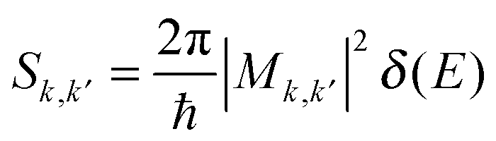
Numerical tools
Scattering rates and lifetimes have been calculated from Fermi's golden rule:where Sk,k′ denotes the probability per unit time of a transition between a given pair of initial and final states labeled by their wave vectors k and k′, respectively. Mk,k′ is the interaction Hamiltonian evaluated between these states. δ(E) implies the overall conservation of energy across the transition. The impact ionization and Auger recombination processes involve two charge carriers. Their initial and final states k and k′ are composite states (k1, k2) and (k1′, k2′). The total scattering rate wk1 for an initiating carrier k1 defined as a conduction electron is given by a threefold summation of Sk,k′ over all partner carriers k2, and all allowed final states (k1′, k2′) fulfilling energy and momentum conservation. Umklapp processes are accounted for, under reciprocal space periodic boundary conditions.
The input for Fermi's golden rule is the electronic structure of phosphorene. It provides (i) the energy-wave vector relation required to evaluate δ(E), and (ii) the associated wave functions required to calculate the interaction strength Mk,k′. The electronic structure of single layer phosphorene has been calculated using density functional theory, as implemented in the Vienna Ab initio Simulation Package within the projector augmented wave framework.36 To correct the semiconductor band gap the underestimation tendency of conventional exchange and correlation functionals, such as LDA or GGA, the PBE0 hybrid exchange and correlation functional has been used.37,38
To discuss the overall effect of impact ionization and Auger recombination on transport properties in phosphorene, other processes such as carrier–phonon scattering and radiative recombination also need to be accounted for. Radiative recombination lifetimes are calculated directly from the electronic structure. The photon polarization is chosen to be parallel to the armchair direction since it exhibits the strongest electron–photon coupling, and consequently the shortest radiative lifetime possible. Other groups have also evidenced this strong anisotropic optical coupling in monolayer10 and bi- or tri-layer phosphorene irrespective of the stacking order.11 At room temperature, carrier–phonon scattering dominates the charge carrier transport, over carrier–impurity scattering,15 and will then serve as a basis for comparison with impact ionization. The determination of carrier–phonon scattering rates requires the phonon dispersion relation. The Einstein and Debye models have been used for the optical and acoustical phonon dispersions, respectively. As presented in ref. 39, the flexural mode is neglected because it would largely be suppressed in a non-freestanding phosphorene flake. The optical phonon energy of 0.055 eV has been estimated from density functional perturbation theory and molecular dynamics calculations presented in ref. 21 and 31. Direction dependent acoustic phonon velocities are taken from ref. 9. Phonon populations are set to room temperature. In our study, carrier–phonon deformation potentials are assumed to be constant and have been determined by fitting the scattering rates to those of Liao et al., which involves more detailed calculations close to the band edges.39
Results
1 Electronic structure
The calculated lattice parameters of 4.54 Å and 3.27 Å along the armchair and zigzag directions agree well with previous computational reports on phosphorene.10,11,13 The calculated 2.2 eV electrical band gap is also in agreement with other calculations, notably using the GW approach to calculate quasi-particle energy levels.11,12,39 Large exciton binding energies (0.7–0.8 eV) have been calculated in phosphorene by solving the Bethe–Salpeter equation.11,12 These results are supported by the 1.45 eV optical band gap measured by photoluminescence,4 and the 2.05 eV electrical band gap measured using scanning tunneling spectroscopy.40 Hence, our band structure calculated using the PBE0 hybrid exchange and correlation functional is relevant to discuss the electronic properties of phosphorene. The conduction band minimum (CBM) and valence band maximum (VBM) are both located at the Γ point. In ref. 39, the conduction and valence bands of phosphorene exhibit a pronounced anisotropy, as shown in Fig. 1 as well. Assuming a parabolic dispersion model, effective masses were extracted from our band structure and are collected in Table 1. In the armchair direction, the effective masses are about 5 times smaller than in the zigzag direction, which indicates a preferential transport along this direction for both electrons and holes under low field conditions. Besides the CBM, the conduction band exhibits a local minimum in the zigzag direction. This satellite valley is located only 0.2 eV above the CBM as shown in Fig. 1. This suggests that a single valley model for the conduction band would not be adapted for the description of electron transport. Indeed, this valley is close enough to the CBM energy that electrons could populate it under moderate electric fields or temperature regimes.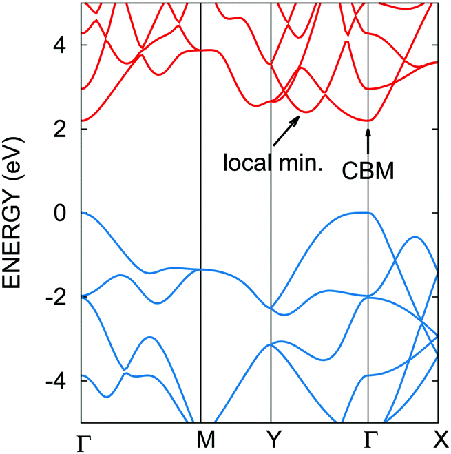 | ||
| Fig. 1 Calculated electronic structure of phosphorene. The band gap is direct at Γ. Anisotropy around the band edges arises between the armchair (Γ–X) and zigzag (Γ–Y) directions. A local minimum lies only 0.2 eV above the conduction band minimum (CBM) in the zigzag direction. | ||
| Armchair | Zigzag | |
|---|---|---|
| VBM | 0.18 | 8.38 |
| CBM | 0.20 | 1.02 |
| Local min. | 0.22 | 0.32 |
2 Impact ionization and carrier–phonon scattering
The calculated impact ionization scattering rates as a function of the initiating carrier energy are shown in Fig. 2a and b, for conduction electrons and valence holes, respectively. The zeros of the energy axis have been set to the CBM and VBM. The rates given as a function of energy are obtained as the sum of the momentum dependent rates wk1, weighted by the initiating carrier density of states. Indeed, impact ionization is a high field process involving a hot impacting electron with a kinetic energy larger than the band gap energy. At such high energies the anisotropy observed close to the band edges is effectively smoothed out due to carrier–phonon scattering. Hence, while being anisotropic in the Brillouin zone, energy averaged rates provide relevant pictures of electron scattering. The impact ionization scattering rates steeply increase beyond the threshold energy, indicating a large increase of the density of final states, for both electron and hole initiated processes. The threshold energy can be extracted by fitting the scattering rates to the Keldysh expression A × ((E − Eth)/Eth)B (see Fig. 2 caption). The calculated threshold energy Eth of 2.28 eV is found to be very close to the band gap energy. This indicates that impact ionization processes could easily take place in phosphorene, without phonon-assisted processes. However, close to the threshold energy, the impact ionization scattering rates seem to be fairly low when compared to the carrier–phonon ones. Our calculations show that the carrier–phonon interaction is generally stronger than impact ionization. This holds for electrons with energies up to 5 eV, and holes with energies up to 4 eV in excess of the band edges. These energies are very high, and correspond to about twice the impact ionization threshold energy. Thus, impact ionization processes are not expected to become dominant over carrier–phonon processes under moderate electric field conditions.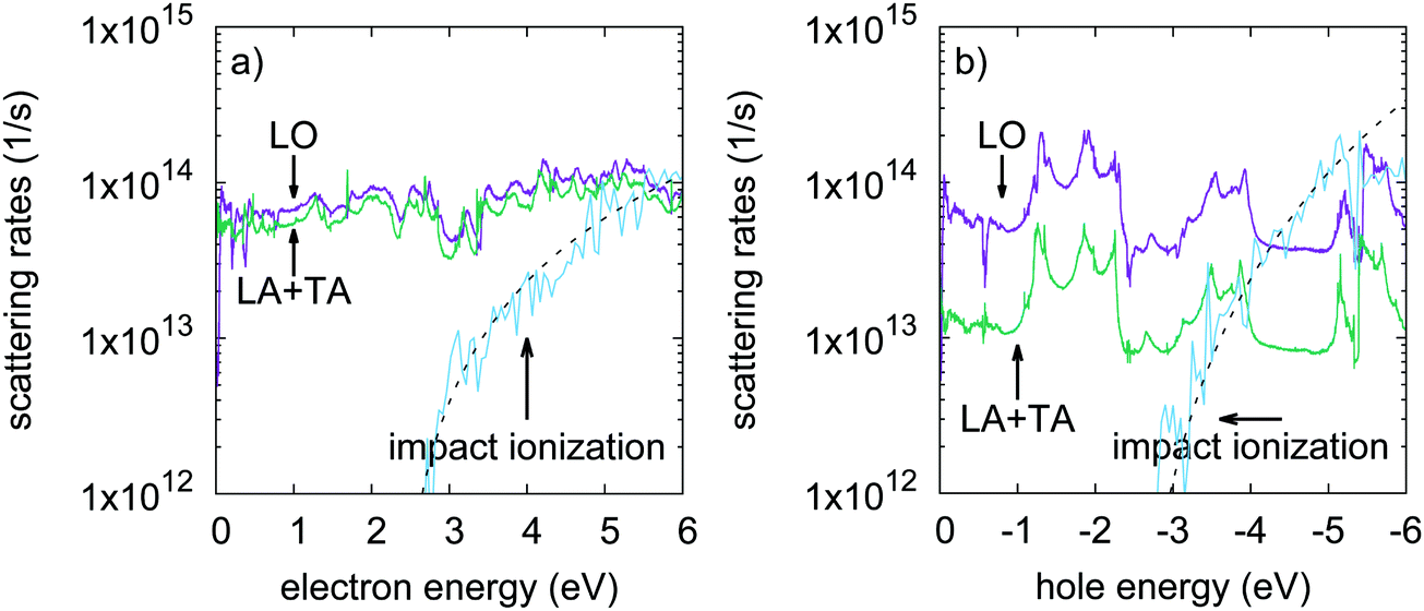 | ||
| Fig. 2 Impact ionization scattering rates as a function of (a) impacting electron energy, and (b) impacting hole energy. Electron–phonon and hole–phonon scattering rates are shown for comparison. The impact ionization rates can be adjusted by A × ((E − Eth)/Eth)B with A = 4.12 × 10¹³, B = 2.05 for electrons, and with A = 6.30 × 10¹³, B = 3.44 for holes (dashed lines). The threshold energy is Eth = 2.28 eV in both cases. | ||
3 Radiative and Auger lifetimes
Minority carrier lifetimes have been calculated and are shown in Fig. 3 for p-type (minority electrons) and n-type (minority holes) phosphorene. Over the investigated doping level range (from 1 × 10¹¹ to 1 × 1014 cm−2), minority electron lifetimes are limited by radiative recombination only, while minority holes transport from a radiatively limited regime to an Auger limited regime for doping densities beyond 1 × 1012 cm−2. This suggests that Auger processes where the recombination energy is given to an electron (eeh processes) are more efficient at recombining electron–hole pairs than processes where the energy is given to a hole (ehh processes). Minority electron radiative lifetimes reach a plateau for doping densities beyond 2 × 1013 cm−2. Indeed, increasing hole density leads to a broader occupation of reciprocal space by holes due to the Pauli exclusion principle and the very small valence band curvature in the zigzag direction. Meanwhile, the conduction band is characterized by larger band curvatures, limiting the spreading of the electron distribution when increasing the electron density. Consequently, the increase in hole density leads to a saturation of the number of direct electron–hole transition channels available for radiative recombination. This saturation phenomenon also takes place for minority holes, and is already reached for majority electron densities as low as 1 × 1011 cm−2. The saturation threshold is lower in the case of minority holes for the same reasons.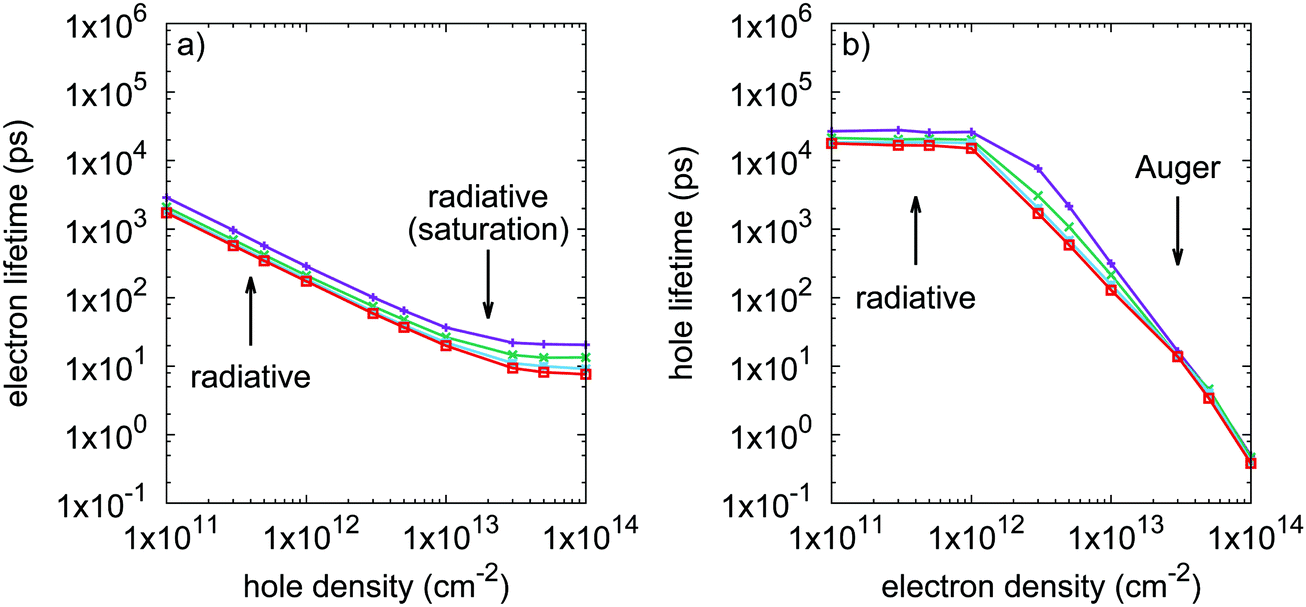 | ||
| Fig. 3 Calculated recombination lifetimes of (a) minority electrons, and (b) minority holes as a function of doping density. Lifetimes for heated carrier populations at 300, 400, 500 and 600 K are shown in purple (+), green (×), blue (square) and red (open square) respectively. | ||
Assuming a frozen band structure, the minority carrier lifetimes have been calculated for carrier distributions between 300 and 600 K. Increasing the charge carrier temperatures tends to shorten lifetimes, since heated carrier distributions can access larger reciprocal space regions using the extra thermal energy. This provides more channels to the heated carriers to fulfill energy and momentum conservation in radiative and Auger recombination processes. However, the temperature increase has no effect on the Auger limited minority hole lifetimes for very large electron densities. Heavily degenerated electron populations already occupy a large region of reciprocal space because of the Pauli exclusion principle, making the temperature effect anecdotic. This is illustrated in Fig. 4, where electron distributions in reciprocal space are given for different values of electron density and temperature. Fig. 4 also shows that increasing the electron density, or the temperature, leads to the occupation of the satellite valley as pointed out in Fig. 1 in the zigzag direction. The occupation of this satellite valley gives electrons access to a larger region of reciprocal space, giving them more channels to fulfill energy and momentum conservation in Auger recombination, and may explain the strength of eeh processes.
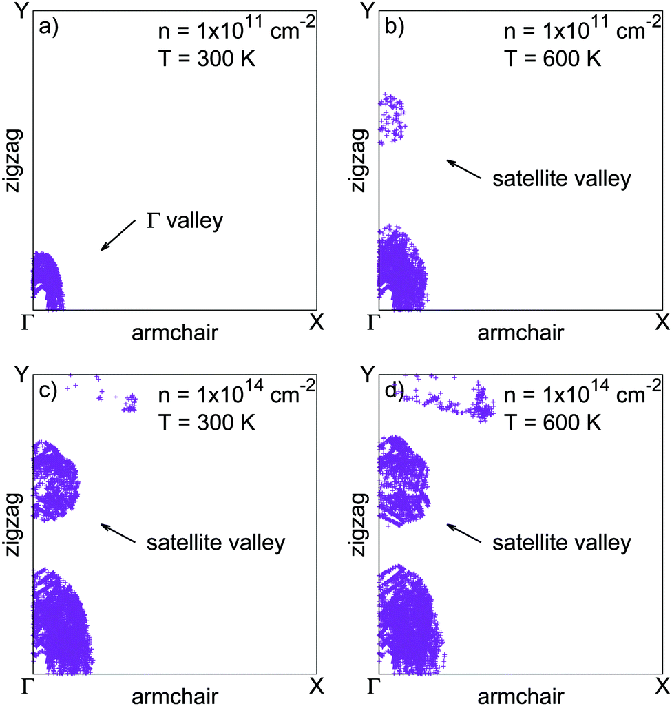 | ||
| Fig. 4 Electron populations shown in the Brillouin zone of phosphorene. Compared to the reference configuration (a), increasing the distribution temperature (b) or the electron density (c) leads to the population of the satellite valley in the zigzag direction. Panel (d) shows the combined effect of high temperature and large electron density on the population of the satellite valley. | ||
In the case of electron–hole pairs created by photo-excitation, additional calculations have been performed with a band gap of 1.7 eV, smaller than the electrical band gap, by manually shifting the bands to simulate exciton binding energies. Similar lifetimes have been obtained, differing by much less than one order of magnitude.
Discussion
1 Electronic devices
In field effect transistors, hot electron injection through the gate dielectric can be followed by impact ionization in the channel. This can lead to local heating, the creation of defects, and ultimately to device failure.32,33 To build ultrathin devices, it has been proposed to use phosphorene as the active material in conjunction with other 2D van der Waals materials such as hexagonal boron nitride (h-BN).10 Successful prototype devices with h-BN as dielectric layers have been reported.16,20 It has been observed that h-BN makes cleaner semiconductor–insulator interfaces compared to commonly used SiO2 dielectrics, and is more resilient to soft dielectric breakdown.41–44 Moreover, h-BN exhibits a large 6 eV band gap, and a high breakdown field (12 MV cm−1) comparable to that of conventional SiO2 dielectrics.44 h-BN is then expected to perform better than SiO2 because it would also protect phosphorene from oxidation and preserve its structure and electronic properties.27 h-BN is considered to be the gate dielectric in this discussion. A large gate bias can cause electron tunneling from the gate electrode, and then lead to the injection of electrons from the h-BN conduction band to the phosphorene layer. This will give birth to hot carriers in phosphorene that can trigger impact ionization. The band alignment between h-BN and phosphorene is difficult to deduce from ref. 10 due to the large smearing used in the calculation of the projected density of states. However, a 2.5 eV barrier can be estimated from the difference in electron affinities. Then, 2.5 eV would also be a lower estimate of the electron excess energy after hot carrier injection. Fig. 2 shows that impact ionization processes would compete with carrier–phonon scattering for hot carriers with excess energies close to or beyond 4 eV. Under very thin dielectric thickness and very large gate bias conditions, such electron excess energies are still possible. This indicates that, although h-BN/phosphorene interfaces seem very promising, hot carrier injection can become problematic for devices with single layer phosphorene/h-BN interfaces under very large electric fields. Multi-layer phosphorene exhibits narrower band gaps than the single layer,12 which would lower their impact ionization threshold energies. Hence, hot carrier injection followed by impact ionization appears to be even more critical for multi-layer phosphorene/h-BN interfaces. In a regime of heavy impact ionization, the extent to which Auger recombination can suppress the newly created electron–hole pairs is not clear, and more details on the charge carrier dynamics are required. However, Fig. 3 shows that electron impact ionization would be more affected by recombination than hole impact ionization because of the shorter recombination lifetimes of the n-type case. In contrast, recombination lifetimes are longer in the p-type case. Consequently, possible hole initiated impact ionization cannot be efficiently compensated by Auger recombination, and can be detrimental to p-type device reliability.2 Optoelectronic devices
Phosphorene has also been proposed as the active material in optoelectronic devices. Its direct band gap and ambipolar transport properties make it an excellent candidate for homojunction optoelectronic devices.15,17 Moreover, pn-homojunctions showing a photovoltaic effect have been experimentally demonstrated.20 To make successful optical emitters or detectors, non-radiative recombination should be avoided. Fig. 3 shows that in p-type phosphorene, charge carrier lifetimes are limited by radiative recombination only, and Auger recombination is not likely to occur. Consequently, phosphorene is a very strong p-type material candidate for optoelectronic devices. Used as an n-type material, phosphorene can still show good optoelectronic properties, although in a limited electron density range. The radiative regime is maintained up to an electron density of 1 × 1012 cm−2 with lifetimes longer than 10 ns. The recombination lifetimes become strongly limited by Auger recombination for electron densities beyond 1 × 1012 cm−2. This would largely impair n-type phosphorene’s optoelectronic properties for heavy electron doping. However, a phosphorene pn-homojunction with tight control of different region widths could lead to LEDs with excellent quantum efficiencies.3 The satellite valley
In phosphorene, p-type transport has already been praised due to its better mobilities and conductivities compared to n-type transport.4,15 In addition, p-type phosphorene has the ability to form ohmic contacts with typical metals such as titanium or gold,15 without having to resort to graphene contacts, which is a technological asset. The poorer n-type transport properties can be explained by (i) larger interaction rates with phonons (compare Fig. 2a and b), and (ii) the presence of a satellite valley only 0.2 eV above the CBM (see Fig. 4). Indeed, the presence of an extra valley close to the conduction band minimum has several implications, as seen in GaAsSb for example.45 First, electrons in the satellite valley have virtually less kinetic energy than in the main valley, because of the 0.2 eV offset. This translates into overall smaller electron velocities than if the material only had a single conduction valley. Second, the satellite valley increases the density of states, and gives birth to intervalley electron transfer. Intervalley scattering randomizes electron momentum, ultimately slowing down the electron population. However, n-type transport can be improved by stress engineering, by modifying effective masses and intervalley energy offsets.7 One can also take advantage of the satellite valley to open new degrees of freedom in optimizing materials for thermoelectric applications. Indeed, conduction band anisotropy can combine a large density of states with high electron mobility. Engineering the density of states via the satellite valley would provide an additional control between doping density and the Fermi level, which can improve the Seebeck coefficient.39Conclusions
Electron and hole scattering rates and lifetimes in single layer phosphorene have been calculated ab initio alongside the electronic structure. Their role and impact under high electric field and heavy doping conditions have been discussed in various device contexts. A very sensitive link between the electronic structure, carrier distribution, scattering rates and lifetimes has been evidenced. It explains the poor n-type conductivity, and predicts that Auger recombination will not be an issue in p-type phosphorene. To further understand the prospects and limitations of phosphorene as an active material in a nanodevice as a function of electrode metals and substrates or encapsulating materials, device level modeling of charge carrier transport is required. Such modeling can be performed using the Ensemble Monte Carlo method, using our results as building blocks. Accounting for various encapsulating materials and the resulting stress conditions could open new degrees of freedom in optimizing the relation between doping and Fermi levels via the satellite valley. These are of interest for thermoelectric applications, in addition to anisotropic electronic and thermal conductivity.Acknowledgements
This work was funded by the Air Force with program name: Aerospace Materials for Extreme Environment and grant number: FA9550-14-1-0157. We acknowledge Advanced Research Computing at Virginia Tech for providing the necessary computational resources and technical support that have contributed to this work (http://www.arc.vt.edu).Notes and references
- F. Schwierz, J. Pezold and R. Granzer, Nanoscale, 2015, 7, 8261 RSC.
- D. Akiwande, N. Petrone and J. Hone, Nat. Commun., 2014, 5, 5678 CrossRef PubMed.
- Z. Guo, H. Zhang, S. Lu, Z. Wang, S. Tang, J. Shao, Z. Sun, H. Xie, H. Wang, X.-F. Yu and P. K. Chu, Adv. Funct. Mater., 2015, 25, 6996 CrossRef CAS.
- H. Liu, A. T. Neal, Z. Zhu, Z. Luo, X. Xu, D. Tomanek and P. D. Ye, ACS Nano, 2014, 8, 4033 CrossRef CAS PubMed.
- F. Xia, H. Wang and Y. Jia, Nat. Commun., 2014, 5, 4458 CAS.
- H. Du, X. Lin, Z. Xu and D. Chu, J. Mater. Chem. C, 2015, 3, 8760 RSC.
- L. Wang, A. Kutana, X. Zou and B. I. Yakobson, Nanoscale, 2015, 7, 9746 RSC.
- Z. Luo, J. Maasen, Y. Deng, Y. Du, R. P. Garrelts, M. S. Lundstrom, P. D. Ye and X. Xu, Nat. Commun., 2015, 6, 8572 CrossRef CAS PubMed.
- S. Lee, F. Yang, J. Suh, S. Yang, Y. Lee, G. Li, H. S. Choe, A. Suslu, Y. Chen, C. Ko, J. Park, K. Liu, J. Li, K. Hippalgaonkar, J. J. Urban, S. Tongay and J. Wu, Nat. Commun., 2015, 6, 9573 Search PubMed.
- T. Hu and J. Hong, ACS Appl. Mater. Interfaces, 2015, 7, 23489 CAS.
- D. Cakir, C. Sevik and F. M. Peeters, Phys. Rev. B: Condens. Matter Mater. Phys., 2015, 92, 165406 CrossRef.
- V. Tran, R. Soklaski, Y. Liang and L. Yang, Phys. Rev. B: Condens. Matter Mater. Phys., 2014, 89, 235319 CrossRef.
- J. Qiao, X. Kong, Z.-H. Hu, F. Yang and W. Ji, Nat. Commun., 2014, 5, 4475 CAS.
- R. Zhang, X. Wu and J. Yang, Nanoscale, 2016, 8, 4001 RSC.
- L. Li, Y. Yu, G. J. Ye, Q. Ge, X. Ou, H. Wu, D. Feng, X. H. Chen and Y. Zhang, Nat. Nanotechnol., 2014, 9, 372 CrossRef CAS PubMed.
- A. Avsar, I. J. Vera-Marun, J. Y. Tan, K. Watanabe, T. Taniguchi, A. H. Castro Neto and B. Ozyilmaz, ACS Nano, 2015, 9, 4138 CrossRef CAS PubMed.
- R. A. Doganov, S. P. Koenig, Y. Yeo, K. Watanabe, T. Taniguchi and B. Ozyilmaz, Appl. Phys. Lett., 2015, 106, 083505 CrossRef.
- S. P. Koenig, R. A. Doganov, H. Schmidt, A. H. Castro Neto and B. Ozyilmaz, Appl. Phys. Lett., 2014, 104, 103106 CrossRef.
- L. Viti, J. Hu, D. Coquillat, W. Knap, A. Tredicucci, A. Politano and M. S. Vitiello, Adv. Mater., 2015, 27, 5567 CrossRef CAS PubMed.
- M. Buscema, D. J. Groenendijk, G. A. Steele, H. S. J. van der Zant and A. Castellanos-Gomez, Nat. Commun., 2014, 5, 4651 CrossRef CAS PubMed.
- R. Fei, A. Faghaninia, R. Soklaski, J. A. Yan, C. Lo and L. Yang, Nano Lett., 2014, 14, 6393 CrossRef CAS PubMed.
- E. Flores, J. R. Ares, A. Castellanos-Gomez, M. Barawi, I. J. Ferrer and and C. Sanchez, Appl. Phys. Lett., 2015, 106, 022102 CrossRef.
- M. Z. Rahman, C. W. Kwong, K. Davey and S. Z. Qiao, Energy Environ. Sci., 2016, 9, 709 CAS.
- Q. H. Wang, K. Kalantar-Zadeh, A. Kis, J. N. Coleman and M. S. Strano, Nat. Nanotechnol., 2012, 7, 699 CrossRef CAS PubMed.
- Y. Guo and J. Robertson, Sci. Rep., 2015, 5, 14165, DOI:10.1038/srep14165.
- K. L. Utt, P. Rivero, M. Mehboudi, E. O. Harriss, M. F. Borunda, A. A. Pacheco SanJuan and S. Barraza-Lopez, ACS Cent. Sci., 2015, 1, 320 CrossRef CAS PubMed.
- R. A. Doganov, E. C. T. O'Farrell, S. P. Koenig, Y. Yeo, A. Ziletti, A. Carvalho, D. K. Campbell, D. F. Coker, K. Watanabe, T. Taniguchi, A. H. Castro Neto and B. Ozyilmaz, Nat. Commun., 2015, 6, 6647 CrossRef CAS PubMed.
- S. Bohloul, L. Zhang, K. Gong and H. Guo, Appl. Phys. Lett., 2016, 108, 033508 CrossRef.
- T.-H. Liu and C.-C. Chang, Nanoscale, 2015, 7, 10648 RSC.
- Y. Hong, J. Zhang, X. Huang and X. C. Zeng, Nanoscale, 2015, 7, 18716 RSC.
- Y.-Y. Zhang, Q. X. Pei, J. W. Jiang, N. Wei and Y. W. Zhang, Nanoscale, 2016, 8, 483 RSC.
- S. Lombardo, J. H. Stathis, B. P. Linder, K. L. Pei, F. Palumbo and C. H. Tung, J. Appl. Phys., 2005, 98, 121301 CrossRef.
- C. Guerin, V. Huard and A. Bravaix, J. Appl. Phys., 2009, 105, 114513 CrossRef.
- B. V. Olson, E. A. Shaner, J. K. Kim, J. F. Klem, S. D. Hawkins, M. E. Flatte and T. F. Boggess, Appl. Phys. Lett., 2013, 103, 052106 CrossRef.
- A. Richter, S. W. Glunz, F. Werner, J. Schmidt and A. Cuevas, Phys. Rev. B: Condens. Matter Mater. Phys., 2012, 86, 165202 CrossRef.
- G. Kresse and D. Joubert, Phys. Rev. B: Condens. Matter Mater. Phys., 1999, 59, 1758 CrossRef CAS.
- J. Paier, R. Hirschl, M. Marsman and G. Kresse, J. Chem. Phys., 2005, 122, 234102 CrossRef PubMed.
- J. P. Perdew, M. Ernzerhof and K. Burke, J. Chem. Phys., 1996, 105, 9982 CrossRef CAS.
- B. Liao, J. Zhou, B. Qiu, M. S. Dresselhauss and G. Chen, Phys. Rev. B: Condens. Matter Mater. Phys., 2015, 91, 235419 CrossRef.
- L. Liang, J. Wang, W. Lin, B. G. Sumpter, V. Meunier and M. Pan, Nano Lett., 2014, 14, 6400 CrossRef CAS PubMed.
- I. Meric, C. R. Dean, N. Petrone, L. Wang, J. Hone, P. Kim and K. L. Shepard, Proc. IEEE, 2013, 101, 1609 CrossRef CAS.
- C. Dean, A. F. Young, L. Wang, I. Meric, G. H. Lee, K. Watanabe, T. Taniguchi, K. Shepard, P. Kim and J. Hone, Solid State Commun., 2012, 152, 1275 CrossRef CAS.
- G.-H. Lee, Y. J. Yu, C. Lee, C. Dean, K. L. Shepard, P. Kim and J. Hone, Appl. Phys. Lett., 2011, 99, 243114 CrossRef.
- Y. Hattori, T. Taniguchi, K. Watanabe and K. Nagashio, ACS Nano, 2015, 9, 916 CrossRef CAS PubMed.
- E. Tea and F. Aniel, J. Appl. Phys., 2011, 109, 033716 CrossRef.
| This journal is © the Owner Societies 2016 |