
 Open Access Article
 This Open Access Article is licensed under a
 Creative Commons Attribution 3.0 Unported Licence
Surface modification of battery electrodes via electroless deposition with improved performance for Na-ion batteries†
Abhishek
Lahiri
*,
Mark
Olschewski
,
René
Gustus
,
Natalia
Borisenko
and
Frank
Endres
*
Institute of Electrochemistry, Clausthal University of Technology, Arnold-Sommerfeld-Str. 6, 38678, Clausthal-Zellerfeld, Germany. E-mail: abhishek.lahiri@tu-clausthal.de; frank.endres@tu-clausthal.de
First published on 10th May 2016
Abstract
Sodium-ion batteries (SIBs) are emerging as potential stationary energy storage devices due to the abundance and low cost of sodium. A simple and energy efficient strategy to develop electrodes for SIBs with a high charge/discharge rate is highly desirable. Here we demonstrate that by surface modification of Ge, using electroless deposition in SbCl3/ionic liquids, the stability and performance of the anode can be improved. This is due to the formation of GexSb1−x at the surface leading to better diffusion of Na, and the formation of a stable twin organic and inorganic SEI which protects the electrode. By judicious control of the surface modification, an improvement in the capacity to between 50% and 300% has been achieved at high current densities (0.83–8.4 A g−1) in an ionic liquid electrolyte NaFSI-[Py1,4]FSI. The results clearly demonstrate that an electroless deposition based surface modification strategy in ionic liquids offers exciting opportunities in developing superior energy storage devices.
Sodium-ion batteries (SIBs) have recently received significant attention in the battery community for large scale energy storage needs due to abundant availability and low cost of sodium.1–3 For SIBs, the potential anode materials are Ge, Sn and Sb which have a theoretical capacity of 369, 847 and 660 mA h g−1, respectively.4–7 Alloys of these materials have also been shown to be promising anode materials.8–13 However, during cycling, all of them show reduced capacity retention primarily due to slow solid-state diffusion of Na ions, unstable solid electrolyte interface (SEI) formation and volume expansion/pulverisation. For example, in the case of germanium thin film anodes, the capacity declined rapidly after 20 to 30 cycles even at low charge/discharge rates of C/10 which has been related primarily due to the change in thin films to a porous morphology or fragmentation of thin films during cycling.14,15 To overcome this issue, we have developed a strategy involving judicious surface modification to produce desired effects on both stability and capacity retention at relatively high charge/discharge current densities.
Surface modification is a versatile technique which has been shown to improve the structural stability, electronic and ionic conductivities as well as suppress surface reactions of the anodes and cathodes for lithium ion batteries.16–19 Various techniques have been applied for surface modification such as sputtering, atomic layer deposition (ALD), sol–gel coating, and mechanical coating, all of which require additional steps as well as additional energy for electrode development.17,19 In comparison, electroless deposition via galvanic displacement reaction does not require any external energy and the surface modification is triggered by a redox reaction. Until now, electroless deposition of noble metals has been used only in lithium-ion batteries to improve the electronic conductivity of anodes such as silicon which was performed in the presence of HF.20–22 It was also found that only after heat treatment of the noble metals on silicon, the capacity fade could be reduced due to the formation of an alloy at the interface.20
Here, we show the surface modification of the electrodeposited amorphous Ge thin film using electroless deposition in a SbCl3/ionic liquid (IL) containing electrolyte to form GexSb1−x at the surface. Fig. 1a and b show the microstructure of the electrodeposited Ge and Ge modified in 0.1 M SbCl3-1-butyl-3-methylpyrrolidinium bis(trifluoromethylsulfonyl)amide (0.1 M SbCl3-[Py1,4]TFSI) by electroless deposition. A change in open circuit potential (OCP) was noted (Fig. S1, ESI†) indicating the electroless deposition of Sb on Ge. However, repeated experiments showed that the change in OCP is not always identical as evident from Fig. S1 (ESI†) and can arise due to the difference in reaction kinetics. The electrodeposited germanium forms a clustered and porous deposit having a cluster size of about 200–300 nm, Fig. 1a.
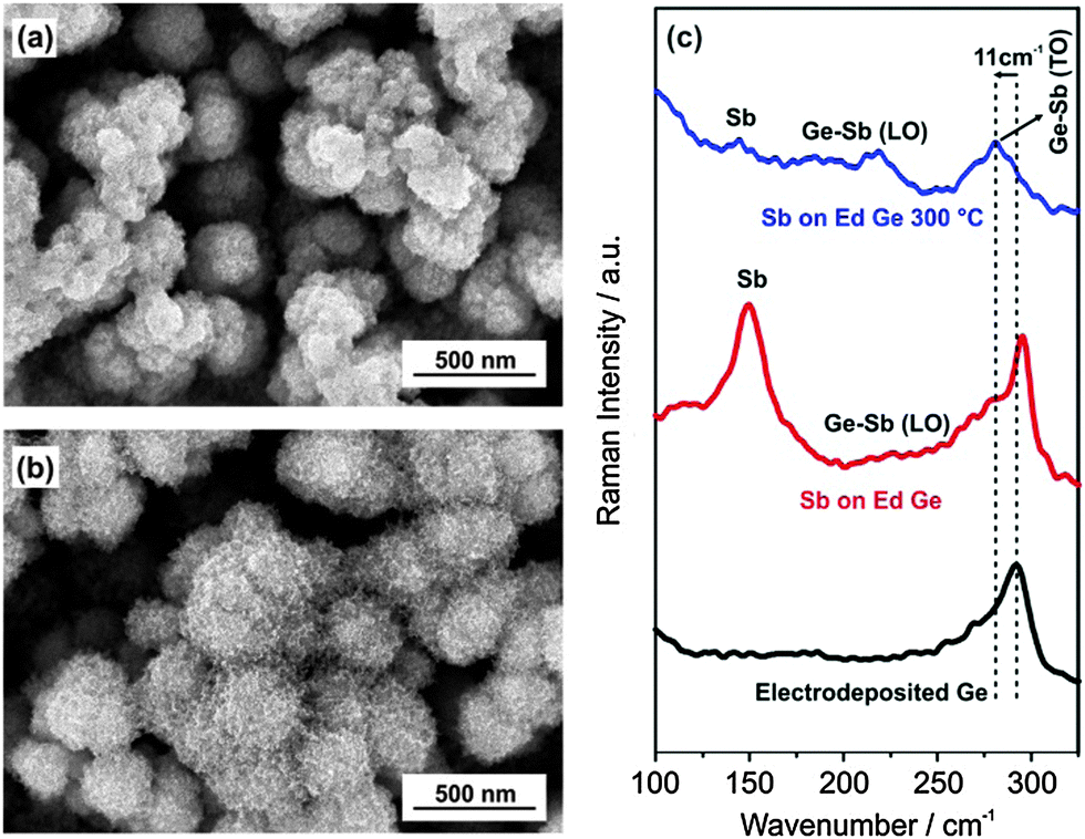 | ||
| Fig. 1 (a) Microstructure of electrodeposited Ge; (b) SEM of electroless deposited Sb on Ge from 0.1 M SbCl3-[Py1,4]TFSI; (c) Raman spectra of electrodeposited Ge (black line), electroless deposited Sb on Ge (red line) and after annealing to 300 °C (blue line). | ||
The Ge clusters are made up of small Ge nanoparticles in the size range of 30–50 nm which has been shown previously.23 The EDX of the electrodeposited Ge (Fig. S2a, ESI†) shows a prominent peak of Ge. Besides, the peaks of O, S and Cl are also seen which is due to exposure of the sample in air during the transfer to the SEM and the presence of some remaining ionic liquids, respectively. Upon modification of the electrodeposited Ge, the presence of Sb nanoparticles on the Ge clusters is evident, Fig. 1b. The EDX spectra (Fig. S2b, ESI†) show prominent peaks of Ge and Sb confirming that electroless deposition occurred and led to surface modification of Ge. X-ray photoelectron spectroscopy (XPS) was also used to probe the surface composition before and after surface modification. The survey scan (Fig. S3, ESI†) of Sb modified Ge shows contributions of both germanium and antimony along with carbon and chlorine in the surface layer. Peak fitting of the Ge 3d (Fig. S4a, ESI†) shows a Ge0 component as well as contributions of GeOx. The XPS spectrum of the Sb 3d structure (Fig. S4b, ESI†) could distinguish the Sb 3d5/2 structure and O 1s. Furthermore the peak fit showed Sb0 as well as Sb3+ and Sb5+ which might be related to SbCl3 and the native oxide layer of the deposit. Thus, from XPS, we can say that GexSb1−x, or a mixture of Ge and Sb phases are present in the Sb modified Ge along with some remaining SbCl3, germanium and antimony oxides.
Raman spectroscopy was also used to evaluate the changes in the Ge nanostructures upon surface modification. In Fig. 1c, electrodeposited Ge shows a Raman peak at 293 cm−1 indicating the presence of amorphous Ge nanoparticles. Surface modification of electrodeposited Ge in 0.1 M SbCl3-[Py1,4]TFSI for 10 minutes led to the formation of Sb A1g vibration mode at 150 cm−1 and a broad peak at 225 cm−1 which relates to the longitudinal optical (LO) phonon vibration of GexSb1−x.24–26 Upon heat treatment of the sample to 300 °C in vacuum, it is evident from Fig. 1c that there is a shift in the Ge peak by 11 cm−1 and the LO phonon vibration peak becomes prominent which confirms the formation of GexSb1−x.
Cyclic voltammetry (CV) of electrodeposited Ge in 1 M sodium bis(fluorosulfonyl)amide/1-butyl-3-methylpyrrolidinium bis(fluorosulfonyl)amide (NaFSI-[Py1,4]FSI) is shown in Fig. 2a. In the first CV cycle, the formation of a solid electrolyte interface (SEI) is seen between +1.5 V and +0.5 V.27 An increase in negative current is observed below +0.5 V and can be related to the sodiation process. In the anodic scan, no desodiation process is observed. However, in the 5th and 10th CV scans, the sodiation process takes place below +0.5 V during the cathodic scan, and a small desodiation wave is observed in the anodic scan at around +0.65 V. This is in contrast to that observed on Ge nanowires with an organic electrolyte wherein no desodiation peaks were observed in the CV cycles.27 The CV cycles on Sb surface modified Ge are shown in Fig. 2b. In the first cycle, the broad reduction peak between +2.5 V and +1.0 V represents the formation of the SEI layer. The sodiation process starts at +0.7 V, which is more positive potential compared to Ge. In the anodic scan, a shoulder is observed at around +0.65 V and a peak is formed at +0.86 V, which can be associated with the desodiation process from Ge and GexSb1−x, respectively. In the 5th and 10th CV cycles, only the sodiation and desodiation processes are seen below +0.75 V and above +0.5 V, respectively.
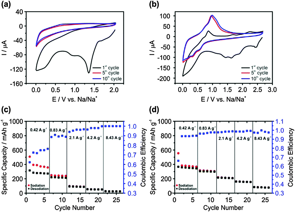 | ||
| Fig. 2 (a) CV of electrodeposited Ge in 1 M NaFSI-[Py1,4]FSI at a scan rate of 1 mV s−1; (b) CV of Sb modified Ge by electroless deposition, in 1 M NaFSI-[Py1,4]FSI at a scan rate of 1 mV s−1; (c and d) charge–discharge cycles at various current densities on electrodeposited Ge and Sb modified Ge, respectively. The first charge–discharge cycle was run at 0.02C to form a stable SEI layer. | ||
The galvanostatic charge–discharge processes at different current densities on electrodeposited Ge are shown in Fig. 2c. It is evident that at 0.42 A g−1 (1C), the specific capacity of sodiation for the first five cycles gives an average value of 376 mA h g−1, which is in good agreement with the theoretical capacity for the formation of NaGe.14 Upon charging and discharging at higher rates, the specific capacity drops significantly, especially at 4.2 (10C) and 8.43 A g−1 (20C) wherein the specific capacity is 52 and 25 mA h g−1, respectively. The increase in coulombic efficiency with a decreased specific capacity indicates that at high charge–discharge rates, the diffusion of Na is limited only to the surface of Ge without any sodiation to the bulk structure. In comparison, on Sb surface modified Ge, it is evident in Fig. 2d that the specific capacity is significantly higher at 4.2 and 8.43 A g−1 with an average value of 160 mA h g−1 and 81 mA h g−1, respectively, which is an increase of more than 300% in Na storage. At a charge–discharge current of 0.83 A g−1, the specific capacity increased from 220 mA h g−1 for electrodeposited Ge to 310 mA h g−1 on Sb modified Ge, which is an increase of about 40% in Na storage. However, not much of a difference is observed in Na storage at 0.42 A g−1. In comparison, the coulombic efficiency is higher in Sb modified Ge at 0.42 A g−1, which indicates that the diffusion of Na is more prominent and therefore at higher charge–discharge currents, a high capacity is achieved compared to Ge. The solid-state diffusion coefficient of Na in Ge is 10−13 cm2 s−1 and is about five orders higher in Sb where it is 10−8 cm2 s−1.27,28 As Ge is modified with Sb nanoparticles and GexSb1−x forms at the interface, the diffusion of Na can take place faster and can intercalate to the bulk of the deposit. To clarify this, galvanostatic charge–discharge cycles were performed on both electrodeposited Ge and Sb modified Ge.
Fig. 3a and b show the charge–discharge profiles of 2nd, 10th and 50th cycles. As repeatable results could not be achieved over 50 cycles for electrodeposited Ge at 0.83 A g−1, experiments were performed at 0.54 A g−1 (1.5C).
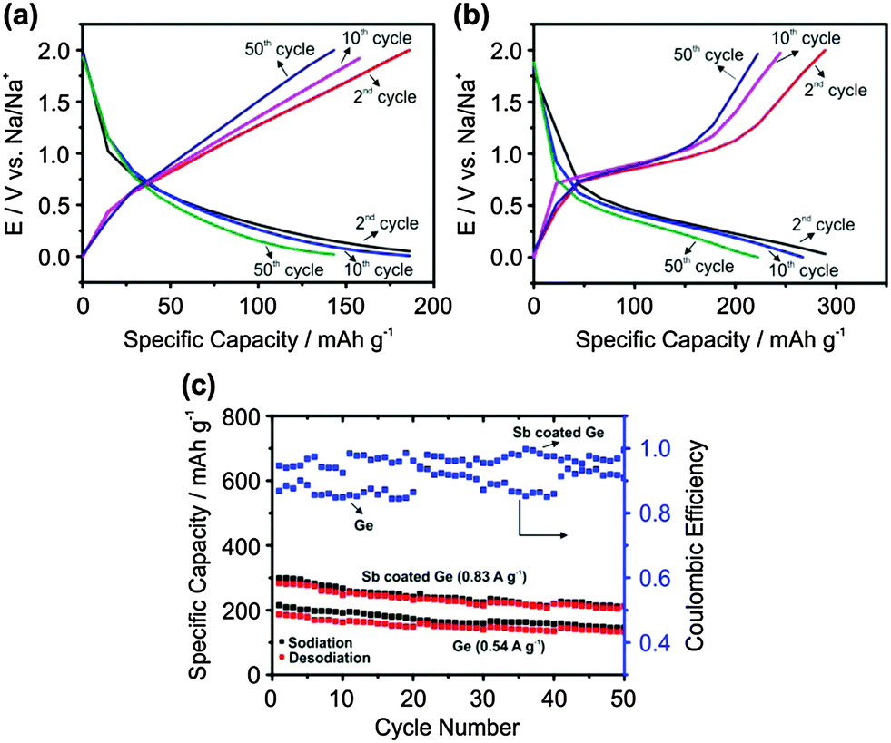 | ||
| Fig. 3 Charge discharge curves for 2nd, 10th and 50th cycles for (a) electrodeposited Ge at 0.54 A g−1; (b) Sb modified Ge at 0.83 A g−1; (c) 50 charge–discharge cycles of electrodeposited Ge and Sb modified Ge. The first charge–discharge cycle was run at 0.02C to form a stable SEI layer. | ||
For electrodeposited Ge, it is evident that the 2nd and 10th cycles show a specific capacity of about 180 mA h g−1, which decreases to 140 mA h g−1 after the 50th cycle. This stability is much superior compared to the previously reported results with Ge thin films which showed degradation to almost zero capacity after 30 cycles at a much lower charge–discharge rate (0.1C).14,15
In comparison, for the Sb modified Ge surface the specific capacity is 290 mA h g−1 for the first cycle and drops to 225 mA h g−1 after the 50th cycle at a charge–discharge current of 0.83 A g−1. Fig. 3c shows the comparison of the charge–discharge processes over 50 cycles for electrodeposited Ge and Sb modified Ge.
Although a higher current density is applied for Sb modified Ge compared to electrodeposited Ge, the specific capacity is higher by at least 50%. In general, with a higher charge–discharge current, the specific capacity decreases. This improvement in the specific capacity as well as higher coulombic efficiency for the Sb modified Ge compared to electrodeposited Ge can be related to the better diffusion of Na ions and the stable formation of the SEI layer.
To evaluate the stability of the SEI layer formed as well as to understand the diffusion of Na ions in Sb modified Ge, X-ray photoelectron spectroscopy (XPS) and Auger electron spectroscopy (AES) were employed. The cycled samples were initially etched by Ar+ ions accelerated to 1 keV in order to remove any residual ionic liquid from the top layer of the surface. The survey spectrum (see Fig. S5, ESI†) compares the cycled samples to the uncycled ones wherein additional peaks of sodium and sulphur are seen for the cycled samples. Fig. 4a–c shows the detailed spectra of Na 1s, F 1s and S 2p transitions for the Sb surface modified germanium (red line) and germanium sample (black line) after cycling.
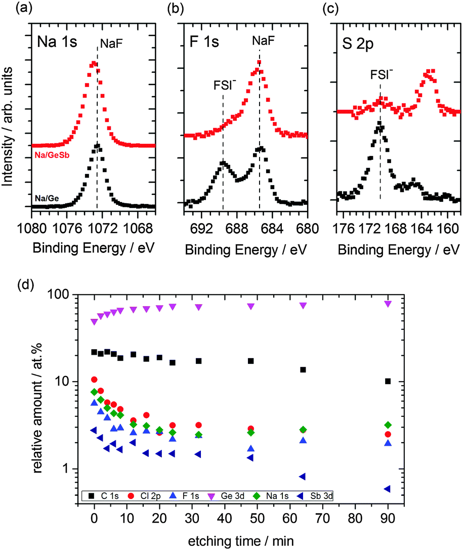 | ||
| Fig. 4 (a–c) XPS detailed spectra (Na 1s, F 1s and S 2p) of electrodeposited Ge (black) and Sb modified Ge (red) after 50 charge–discharge cycles in 1 M NaFSI-[Py1,4]FSI; (d) stoichiometry of surface components from XPS survey spectra after sputter etching with 2 keV Ar+ ions for Sb modified Ge sample after cycling. | ||
The symmetric peak shape of Na 1s in Fig. 4a indicates sodium compounds, rather than metallic sodium, and is emphasized by a prominent NaF29 peak at 685.6 eV binding energy (BE) in the F 1s detail spectrum (Fig. 4b). The sodiated Ge additionally shows contributions from FSI at 689.4 eV BE. Contributions of FSI could be observed for the Sb modified Ge sample, too. However, a significant difference in the S 2p spectrum is observed upon comparing the sodiation process in Ge and Sb modified Ge. The S 2p spectrum in Fig. 4c reveals a shoulder at 165.3 eV BE for the Ge sample and a peak at 162.8 eV BE. The peak at 162.8 eV BE can be assigned to sodium sulphide30 and the shoulder at 165.3 eV BE is most likely sodium sulphate which might have formed due to the reduction of FSI in the presence of sodium ions.31 Upon analysing the Sb spectra (Fig. S6, ESI†) before and after cycling, a significant difference is observed. The Sb3+ and Sb5+ peaks have diminished along with Sb 3d3/2 and a clear Na KLL and O 1s peak can be distinguished. This suggests that a relatively thick SEI layer is formed and Na has intercalated into the Sb layer and probably reduces the oxide species of Sb during intercalation. The presence of O 1s could be due to the formation of Na2O. A similar reduction process was seen during Na intercalation in TiO2.32
Subsequently the cycled antimony modified Ge sample was etched with 2 keV Ar+ ions in several steps, each verified by XPS survey spectra. The peak areas were normalized by photoelectric cross-sections, asymmetry factors and transmission functions of the hemispherical analyzer to calculate the stoichiometry of the surface components. Although the actual sputter rate depends on various effects (on the matrix and molecular level) the stoichiometric data were plotted against sputter time in Fig. 4d to give a semi-quantitative insight of the composition with depth. It is evident that the relative amount of germanium increases within the first 20 minutes of etching, whereas that of the other components like carbon, chlorine, fluorine, antimony and sodium decreases. Between 20 and 50 minutes of sputtering, the Na concentration plateaus and slightly increases upon further sputtering, whereas Sb concentration decreases significantly after 50 minutes of sputtering. This indicates that Na not only has intercalated to the outer layers, but also has intercalated to the bulk of Ge.
Further investigation of the SEI layer after the first sodiation process showed the formation of a thin inorganic SEI layer on the Sb modified Ge and an organic outer layer. A large area image showing the formation of the SEI layer is shown in Fig. S7 (ESI†). Fig. 5a shows the SEM image of Sb modified Ge after the first full charge. The image reveals two different structured deposits, a thick cauliflower-like deposit (A) and a comparatively thin layer (B). The respective Auger electron spectroscopy (AES) data are shown in Fig. 5b. While both spectra show distinctive peaks, which can be assigned to sulphur (S LMM), chlorine (Cl LMM), carbon (C KLL), oxygen (O KLL) and fluorine (F KLL); significant amounts of antimony (Sb MNN), germanium (Ge LMM) and sodium (Na KLL) can only be found for the thin layer (B). The formation of the inorganic–organic SEI layers has been shown to be advantageous for Li–air batteries wherein the Li dendritic growth could be avoided, thereby resulting in an enhanced coulombic efficiency.33
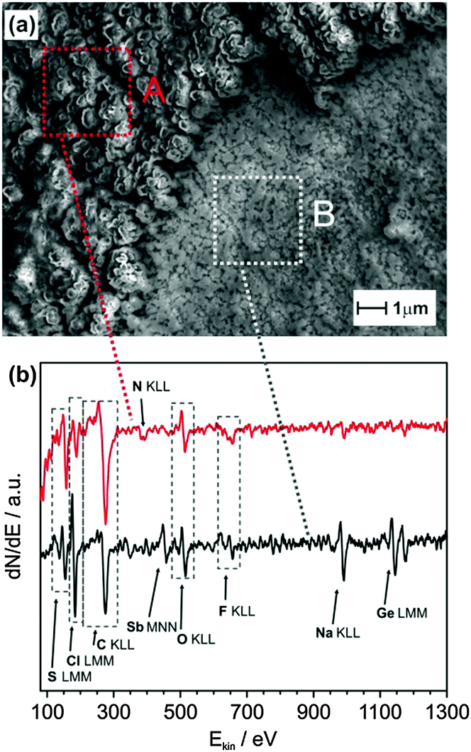 | ||
| Fig. 5 (a) SEM image of Sb modified Ge after the first sodiation process recorded at a beam energy of 5 kV; (b) AES spectra of the regions marked in the SEM image. | ||
Thus, from the XPS and AES results, it appears that on Sb modified Ge, a better SEI layer is formed which is made up of primarily sodium compounds (NaF, Na2S) in the inner layer compared to the presence of higher concentrations of decomposed ionic liquids along with sodium compounds for Ge. The presence of sodium compounds would result in faster sodium diffusion through the SEI layer, whereas the outer organic SEI layer protects the electrode from further reacting with the electrolyte during the charge–discharge processes. Also, as GexSb1−x is formed (shown by Raman spectroscopy) on the Sb modified Ge surface, it might have created defects in the Ge structure during galvanic displacement reaction, resulting in faster diffusion of Na ions in Ge as exemplified by the depth profile analysis in Fig. 4d. These two factors have resulted in improved charge storage and battery performance at higher charge densities for Sb modified Ge.
Conclusions
In conclusion, we have demonstrated a versatile technique of surface modification of a germanium electrode using electroless deposition from ionic liquids at room temperature. The surface modification led to improved capacity and stability of the Na-ion batteries at high charge/discharge current densities with an ionic liquid electrolyte. The present findings open up new paradigms for creating and modifying anodic materials for rechargeable batteries.Acknowledgements
The authors would like to thank Mrs Karin Bode, Institute of Inorganic Chemistry (Prof. A. Adam) for help with Raman measurements and Prof. W. Daum for providing the NanoSAM (Omicron NanoSAM provided by: Deutsche Forschungsgesellschaft DFG, grant number: INST 189/158-1). The authors would also like to thank Celgard for providing the membrane.Notes and references
- H. Pan, Y.-S. Hu and L. Chen, Energy Environ. Sci., 2013, 6, 2338 CAS.
- N. Yabuuchi, K. Kubota, M. Dahbi and S. Komaba, Chem. Rev., 2014, 114, 11636 CrossRef CAS PubMed.
- D. Kundu, E. Talaie, V. Duffort and L. F. Nazar, Angew. Chem., Int. Ed., 2015, 54, 3431 CrossRef CAS PubMed.
- Y. Kim, K.-H. Ha, S. M. Oh and K. T. Lee, Chem. – Eur. J., 2014, 20, 11980 CrossRef CAS PubMed.
- M. Dahbi, N. Yabuuchi, K. Kubota, K. Tokiwa and S. Komaba, Phys. Chem. Chem. Phys., 2014, 16, 15007 RSC.
- Z. Li, J. Ding and D. Mitlin, Acc. Chem. Res., 2015, 48, 1657 CrossRef CAS PubMed.
- H. Kang, Y. Liu, K. Cao, Y. Zhao, L. Jiao, Y. Wang and H. Yuan, J. Mater. Chem. A, 2015, 3, 17899 CAS.
- B. Farbod, K. Cui, W. P. Kalisvaart, M. Kupsta, B. Zahiri, A. Kohandehghan, E. M. Lotfabad, Z. Li, E. J. Luber and D. Mitlin, ACS Nano, 2014, 8, 4415 CrossRef CAS PubMed.
- P. R. Abel, M. G. Fields, A. Heller and C. B. Mullins, ACS Appl. Mater. Interfaces, 2014, 6, 15860 CAS.
- J. Hur and I. T. Kim, Bull. Korean Chem. Soc., 2015, 36, 1625 CrossRef CAS.
- N. Lin, J. Zhou, Y. Han, K. Zhang, Y. Zhu and Y. Qian, Chem. Commun., 2015, 51, 17156 RSC.
- Y. Xu, X. Zhu, X. Zhou, X. Liu, Y. Liu, Z. Dai and J. Bao, J. Phys. Chem. C, 2014, 118, 28502 CAS.
- L. Hu, X. Zhu, Y. Du, Y. Li, X. Zhou and J. Bao, Chem. Mater., 2015, 27, 8138 CrossRef CAS.
- L. Baggetto, J. K. Keum, J. F. Browning and G. M. Veith, Electrochem. Commun., 2013, 34, 41 CrossRef CAS.
- P. R. Abel, Y.-M. Lin, T. de Souza, C.-Y. Chou, A. Gupta, J. B. Goodenough, G. S. Hwang, A. Heller and C. B. Mullins, J. Phys. Chem. C, 2013, 117, 18885 CAS.
- T.-F. Yi, Y.-R. Zhu, X.-D. Zhu, J. Shu, C.-B. Yue and A.-N. Zhou, Ionics, 2009, 15, 779 CrossRef CAS.
- A. Mauger and C. Julien, Ionics, 2014, 20, 751 CrossRef CAS.
- L. J. Fu, H. Liu, C. Li, Y. P. Wu, E. Rahm, R. Holze and H. Q. Wu, Solid State Sci., 2006, 8, 113 CrossRef CAS.
- K.-X. Wang, X.-H. Li and J.-S. Chen, Adv. Mater., 2015, 27, 527 CrossRef CAS PubMed.
- J. W. Kim, J. H. Ryu, K. T. Lee and S. M. Oh, J. Power Sources, 2006, 147, 227 CrossRef.
- M. Thakur, M. Isaacson, S. L. Sinsabaugh, M. S. Wong and L. J. Biswal, J. Power Sources, 2012, 205, 426 CrossRef CAS.
- W. McSweeney, H. Geaney and C. O'Dwyer, Nano Res., 2015, 8, 1395 CrossRef CAS.
- A. Lahiri, S. Zein El Abedin and F. Endres, J. Phys. Chem. C, 2012, 116, 17739 CAS.
- C. C. Huang, B. Gholipour, K. Knight, J. Y. Ou and D. W. Hewak, Adv. OptoElectron., 2012, 840348, 1 CrossRef.
- Q. H. F. Rebelo, E. A. Cotta, S. M. de Souza, D. M. Trichês, K. D. Machado, J. C. de Lima, T. A. Grandi, C. M. Poffo and L. Manzato, J. Alloys Compd., 2013, 575, 80 CrossRef CAS.
- T. Nakagawa, K. Ohta and N. Koshizuka, Jpn. J. Appl. Phys., 1980, 19, L339 CrossRef CAS.
- A. Kohandehghan, K. Cui, M. Kupsta, J. Ding, E. M. Lotfabad, W. P. Kalisvaart and D. Mitlin, Nano Lett., 2014, 14, 5873 CrossRef CAS PubMed.
- L. Baggetto, P. Ganesh, C.-N. Sun, R. A. Meisner, T. A. Zawodzinski and G. M. Veith, J. Mater. Chem. A, 2013, 1, 7985 CAS.
- W. E. Morgan, J. R. Van Wazer and W. J. Stec, J. Am. Chem. Soc., 1973, 95, 751 CrossRef CAS.
- K. M. Abraham and S. M. Chaudhri, J. Electrochem. Soc., 1986, 133, 1307 CrossRef CAS.
- S. Xiong, S. K. Xie, E. Blomberg, P. Jacobsson and A. Matic, J. Power Sources, 2014, 252, 150 CrossRef CAS.
- L. Wu, D. Bresser, D. Buchholz, G. A. Giffin, C. R. Castro, A. Ochel and S. Passerini, Adv. Energy Mater., 2015, 5, 1401142 Search PubMed.
- X.-B. Cheng, R. Zhang, C.-Z. Zhao, F. Wei, J.-G. Zhang and Q. Zhang, Adv. Sci., 2016, 3, 1500213 Search PubMed.
Footnote |
| † Electronic supplementary information (ESI) available. See DOI: 10.1039/c6cp02364a |
| This journal is © the Owner Societies 2016 |