
 Open Access Article
 This Open Access Article is licensed under a Creative Commons Attribution-Non Commercial 3.0 Unported Licence
Fabrication of Ti substrate grain dependent C/TiO2 composites through carbothermal treatment of anodic TiO2†
Celine
Rüdiger‡
*ab,
Marco
Favaro§
c,
Carlos
Valero-Vidal¶
b,
Laura
Calvillo
c,
Nathalie
Bozzolo
d,
Suzanne
Jacomet
d,
Clivia
Hejny
e,
Luca
Gregoratti
f,
Matteo
Amati
f,
Stefano
Agnoli
c,
Gaetano
Granozzi
c and
Julia
Kunze-Liebhäuser
*b
aPhysik-Department, Technische Universität München, James-Franck-Str. 1, 85748 Garching, Germany. E-mail: Celine.Ruediger@uibk.ac.at; Tel: +43 (0) 512 507 58018
bInstitut für Physikalische Chemie, Leopold-Franzens-Universität Innsbruck, Innrain 52c, 6020 Innsbruck, Austria. E-mail: Julia.Kunze@uibk.ac.at; Tel: +43 (0) 512 507 58013
cDipartimento di Scienze Chimiche, Università di Padova, Via Marzolo 1, 35131 Padova, Italy
dMINES ParisTech, PSL – Research University, CEMEF – Centre de Mise en Forme des Matériaux, CNRS UMR 7635, CS 10207 Rue Claude Daunesse, 06904 Sophia Antipolis Cedex, France
eInstitut für Mineralogie und Petrographie, Leopold-Franzens-Universität Innsbruck, Innrain 52d, 6020 Innsbruck, Austria
fElettra – Sincrotrone Trieste SCpA, SS14-Km163.5 in Area Science Park, 34149 Trieste, Italy
First published on 1st March 2016
Abstract
Composite materials of titania and graphitic carbon, and their optimized synthesis are highly interesting for application in sustainable energy conversion and storage. We report on planar C/TiO2 composite films that are prepared on a polycrystalline titanium substrate by carbothermal treatment of compact anodic TiO2 with acetylene. This thin film material allows for the study of functional properties of C/TiO2 as a function of chemical composition and structure. The chemical and structural properties of the composite on top of individual Ti substrate grains are examined by scanning photoelectron microscopy and micro-Raman spectroscopy. Through comparison of these data with electron backscatter diffraction, it is found that the amount of generated carbon and the grade of anodic film crystallinity correlate with the crystallographic orientation of the Ti substrate grains. On top of Ti grains with ∼(0001) orientations the anodic TiO2 exhibits the highest grade of crystallinity, and the composite contains the highest fraction of graphitic carbon compared to Ti grains with other orientations. This indirect effect of the Ti substrate grain orientation yields new insights into the activity of TiO2 towards the decomposition of carbon precursors.
1. Introduction
Composite materials of titania and conductive graphitic carbon have gained particular research interest for application in photocatalysis, dye sensitized solar cells (DSSCs), Li-ion batteries and proton exchange membrane fuel cells (PEMFCs) due to the enhanced performance of the composite compared to TiO2 or C alone.1–5 It was shown that the application-specific performance of C/TiO2 hybrid materials is highly sensitive to the synthesis route6 and the detailed preparation conditions.1,7,8 There is evidence that the major benefits of functional C/TiO2 nanocomposites, such as their superior stability and electric conductivity, rely on a close contact between conductive carbon and TiO2.9,10 Hence, an adapted synthesis is of vital importance to optimize application-specific functional properties.Biphasic C/TiO2 or mixed TiOxCy (rich in TiC/TiO) materials with different morphologies, such as nanotubes, nanoparticles or thin films, can be prepared via carbothermal treatment of initially prepared titania precursors with reactive acetylene (C2H2) in a gas flow reactor.11–15 These materials have been tested as catalyst supports in studies of the electrochemical reduction of oxygen11 or oxidation of small alcohols,12,16,17 and as Li-ion battery anodes,15 and exhibited promising performances. The employed carbothermal route provides realistic process conditions that are relevant for the production of high surface area functional materials based on TiO2 and C. The physico-chemical properties of the thus prepared materials are empirically tailored via the synthesis parameters. An adapted design of functional composites requires a detailed understanding of the correlation between the synthesis conditions and the intrinsic physico-chemical properties of the produced materials.
In this context, planar anodic titania films that are carbothermally treated under reproducible conditions can be used to systematically study the synthesis–property–performance relationships, which are essential to identify the optimal synthesis procedure to obtain specific functional materials via the carbothermal route. Anodic films are particularly interesting due to their tunable morphology, which can be varied from compact films18 to high aspect ratio self-organized nanotubes.19 Several studies have been performed on carbothermally reduced compact anodic TiO2, rich in TiO and TiC phases, to correlate the synthesis conditions with intrinsic physico-chemical properties, such as structure and composition, and with functional performance, such as (electro-)chemical stability or electrical conductivity.14,16,17,20
In a previous study, we have shown that the synthesis conditions of TiOxCy films14 significantly influence the catalytic activity of thereon deposited Pt nanoparticles towards the electro-oxidation of ethanol. Interestingly, it was found that the electrochemical stability of Pt/TiOxCy appeared to be affected by the grain orientations of the polycrystalline Ti substrate.16 This indicates that the texture of the Ti substrate, on which the precursor anodic film is prepared, constitutes an additional parameter that has to be taken into account when optimizing the synthesis of TiOxCy films.
In view of the importance of C/TiO2 composites for applications in energy conversion and storage, we present a study on the preparation of a thin carbon film on compact anodic TiO2 on polycrystalline Ti (C/TiO2/Tipoly) by means of carbothermal treatment with C2H2 in a flow reactor at 550 °C. A special focus is given to the investigation of the substrate grain dependent physico-chemical properties of the C/TiO2 composite film.
The films are ex situ characterized by means of local analysis tools. Electron backscatter diffraction (EBSD), micro-Raman spectroscopy, scanning electron microscopy (SEM), atomic force microscopy (AFM) and scanning photoelectron microscopy (SPEM) are used to correlate grain orientations of the polycrystalline Ti substrate with the local crystalline phase composition, surface topography and chemical composition of the C/TiO2 films.
The present study sheds light on the origin of the substrate grain effect in carburized TiO2/Tipoly systems and thereby shows the significance of the TiO2 precursor properties for the synthesis of optimized functional C/TiO2 composites via the carbothermal route.
2. Experimental section
Disks of 1 mm thickness and diameters of 10–15 mm were cut from a 20 mm diameter polycrystalline Ti rod (99.6% purity, temper annealed, Advent Ltd, England). One side of the sample was mechanically and electrochemically polished, following the procedure described in ref. 14 (see the detailed description in the ESI†). To enable the retrieval of identical spots on the samples, a cross-scratch was placed as a marker in the center of the electropolished area by using a tungsten needle.The crystallographic texture of the electropolished Ti substrate was mapped by EBSD (see Fig. 1) using a FEI XL30 scanning electron microscope (SEM) operated at 20 kV accelerating voltage and equipped with a TSL-EDAX EBSD system. The step size of the EBSD map was set to 2 μm, which led to a suitable spatial resolution of the microstructure.
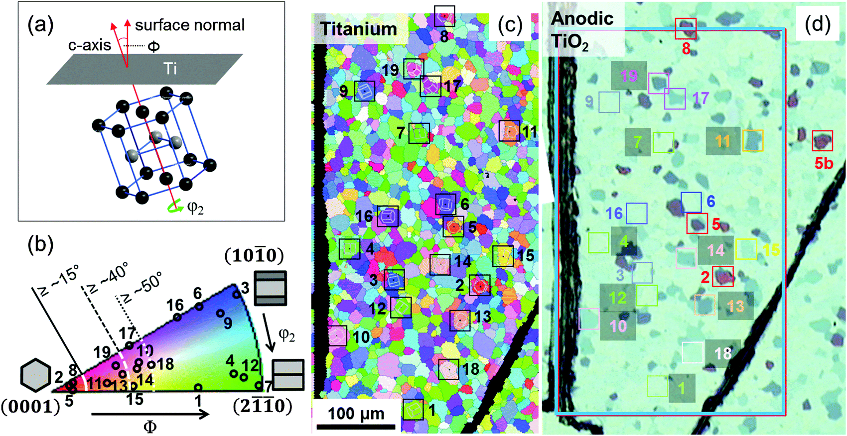 | ||
| Fig. 1 (a) Schematic sketch of the orientation of the hexagonal lattice of Ti with respect to the Ti substrate surface. (b) Standard triangle of the surface-normal projected inverse pole figure orientation map (EBSD map) with numbers of the studied grains, ranges of tilt-angles Φ and the surface projected hexagonal cells. (c) EBSD map of a Ti substrate; (d) optical micrograph of the surface area shown in (c) after anodization. | ||
The electropolished Ti samples were consecutively cleaned in an ultrasonic bath with ethanol (technical grade), isopropanol (high purity) and de-ionized (DI) water (Millipore-Milli-Q system, 18.2 MΩ). Compact amorphous TiO2 films were produced by potentiostatic electrochemical anodization in a home-built Teflon electrochemical cell with a two-electrode configuration using a DC power supply controlled by a multimeter, and applying the following settings: anodization at 20 V for 600 s in 0.1 M sulfuric acid (H2SO4, analytical grade, 95–97%, Merck, Germany) electrolyte at room temperature using a platinum mesh counter electrode.14 The anodic films were rinsed with DI water and dried in an argon (Ar 4.8, Linde, Germany) stream.
A carbon layer was synthesized on the anodic film by carbothermal treatment in a tubular quartz reactor under controlled gas flow. The gas flow and acetylene dose were optimized for the reactor geometry. In a reactor tube of 40 mm diameter, the following procedure was applied: [i] purged for two hours under a high flow of Ar to remove air, [ii] heated for up to 90 min at a constant rate to 550 °C in 200 standard cubic centimeters per minute (sccm) Ar, [iii] maintained for 60 min at 550 °C, [iv] 0.5 flow% of acetylene (C2H2, solvent-free, Linde, Germany) was added for 5 min, [v] maintained for 60 min at 550 °C in Ar, and [vi] the oven was left to cool down to room temperature. These samples will be referred to as C/TiO2. A reference sample (termed TiOref2) was thermally treated in 200 sccm Ar without C2H2 according to the sequence [i]–[ii]–[v]–[vi].
After anodization and thermal treatment, optical micrographs were acquired for the reference sample using a camera of 10× magnification (belonging to the AFM equipment). The surface morphology of TiO2 and C/TiO2 was investigated using a field emission SEM based on a GEMINI column in a Zeiss CrossBeam NVision 40 system. Micrographs were acquired with the in-lens secondary electron detector using an acceleration voltage of 4 kV and working distances of 4–7 mm. AFM was performed as described in the ESI.†
Micro-Raman spectroscopy was applied to investigate the crystalline phase composition of C/TiO2 and TiOref2. A Jobin Yvon Horiba HR800 instrument equipped with a Nd:YAG laser (532 nm) was used in a non-focal operation mode and without a polarizer to analyze the average chemical composition and structure of the film on top of individual Ti substrate grains. The size of the focused laser spot on the sample was about 5 μm using the 50× magnification of the optical microscope. Backscattered Raman signals were recorded with a resolution of less than 2 cm−1 (as determined by measuring the Rayleigh line) in a spectral range from 80 to 2000 cm−1.
SPEM was performed at the ESCAmicroscopy beamline at the Elettra Synchrotron Facility in Trieste, where the X-ray photon beam was demagnified by a Zone Plate to a sub-micron spot of about 150 nm onto the sample, which was then rastered to produce an image by detecting the photoelectrons generated from the sample.21 In this work the photon energy was set to 756 eV. The incident X-ray beam was normal to the sample surface while the angle between the hemispherical electron analyzer (HEA) and the sample surface was 30°. Photoelectron maps of 50 × 50 μm2 were recorded by sampling the surface with a step of 0.2 μm and a dwelling time of 60 ms per pixel. The HEA was equipped with a multichannel electron detector which simultaneously acquires 48 maps (channels), each tuned to a specific photoelectron energy within a selected energy window. This allowed the (i) extraction of spectra from a selected area of the acquired photoelectron micrograph with an energy window of 7.8 eV and a step of 0.164 eV and (ii) removal of the topographic contributions to the photoelectron micrographs and extraction of the chemical contrast. The chemical contrast micrographs (chemical maps) were obtained by selecting, from the recorded 48 maps, those acquired at the photoelectron peak energy and those acquired at an energy related to the background of the photoelectron peak, integrating them to obtain two maps corresponding to the photoelectron peak and background intensity, and determining their ratio.22 The ratio of photoelectron maps acquired in the spectral regions of the C 1s and Ti 2p core levels with their corresponding background is referred to as C/BG and TiO2/BG, respectively. For elemental analysis of the C/TiO2 composite, the uncorrected absolute peak area was used as a qualitative measure, which was obtained from integration of the spectra from the image after subtraction of a constant background.
Additional information about the performed experiments can be found in the ESI.†
3. Results
3.1 Identification of substrate grain orientations
The crystallographic orientations of the Ti substrate grains are determined by EBSD, which provides the three Euler angles, φ1, Φ and φ2, which define the crystallographic orientation of the hexagonal unit cell with respect to the substrate surface (according to the Bunge convention23). The sketch in Fig. 1 illustrates the orientation of the hexagonal lattice24 with respect to the substrate surface: Φ gives the tilt angle of the unit cell c-axis with respect to the surface normal and φ2 gives the azimuthal rotation of the hexagonal unit cell around its c-axis.23,25 A rotation of the Ti substrate around its surface normal is described by the angle φ1 (not shown in Fig. 1). The two Euler angles Φ and φ2 can be restricted to 0° ≤ Φ ≤ 90° and 0° ≤ φ2 ≤ 30° due to the symmetry of the hexagonal lattice. For the azimuthal rotation the zero point is chosen to coincide with the (10![[1 with combining macron]](https://www.rsc.org/images/entities/char_0031_0304.gif) 0) plane for Φ = 90°, while φ2 = 30° and Φ = 90° yield the (20) plane. The crystallographic orientation of individual substrate grains can be illustrated in a surface-normal projected inverse pole figure orientation map (from now on termed EBSD map) like in Fig. 1c that uses an RGB color code defined in the standard triangle in Fig. 1b. From the colors in the standard triangle the crystallographic direction parallel to the sample surface normal can be deduced.
0) plane for Φ = 90°, while φ2 = 30° and Φ = 90° yield the (20) plane. The crystallographic orientation of individual substrate grains can be illustrated in a surface-normal projected inverse pole figure orientation map (from now on termed EBSD map) like in Fig. 1c that uses an RGB color code defined in the standard triangle in Fig. 1b. From the colors in the standard triangle the crystallographic direction parallel to the sample surface normal can be deduced.
EBSD and optical microscopy are used to generate a correlation map between the Ti substrate grain orientation and the optical appearance of the anodic oxide film. Fig. 1 shows the EBSD map of an electropolished titanium substrate and an optical micrograph of the same surface after anodization. According to ellipsometry measurements (not shown), the fresh anodic TiO2 film has an average thickness of ∼53 nm. The comparison of Fig. 1c and d reveals that the interference colors of the anodic TiO2 are strongly affected by the orientation of the Ti substrate grains. In particular, the substrate tilt angle Φ has an important impact on the optical properties of the oxide film. Variations in interference properties are directly related to variations in the TiO2 film thickness. Under the applied synthesis conditions, dark colors correspond to thinner films, and bright colors to thicker TiO2 films.26,27 We can define four ranges of substrate tilt angles Φ that cause different interference colors of the oxide film (see Fig. 1b). The azimuthal substrate orientation, described by φ2, has only a minor effect on the interference colors of the anodic film (see ESI†). Due to the rotational symmetry of the oxide film thickness on individual grains, the corresponding orientation angle φ1 does not affect the interference color of the anodic TiO2. Table 1 summarizes the assignment of the oxide colors to the tilt angles Φ of the Ti substrate. This allows an estimation of the substrate orientations without the necessity of an EBSD measurement. The two orientations ∼Ti{100} (φ2 ∼ 0°) and ∼Ti{20} (φ2 ∼ 30°) can be deduced (without EBSD map) from the optical appearance of the anodic film after thermal treatment at 550 °C (see Fig. S1 and the discussion in ESI†).
| Interference color (thickness) of TiO2 | Dark red (thin TiO2) | Dark violet/blue | Blue | Bright blue (thick TiO2) | |
|---|---|---|---|---|---|
| a See also ESI. | |||||
| Tilt angle Φ of Ti | 0° ≤ Φ ≤ ∼15° | ∼15° ≤ Φ ≤ ∼40° | ∼40° ≤ Φ ≤ ∼50° | Φ ≥ ∼50° (i.e. all ∼Ti{hki0}) | |
| Ti(hkil)a | ∼Ti(0001) | ∼Ti{100} |
∼Ti{20} |
||
| EBSD map colors | Red | Pink-orange | Purple-yellow | Blue | Green |
| Representative hexagonal cell |

|

|
|

|

|
In the following, we will focus on the relationship of local chemical and physical properties, obtained by microscopic and spectroscopic techniques of planar C/TiO2/Tipoly composite materials, and the tilt angle Φ of the Ti substrate grains. The restriction to Φ is motivated by studies of the TiO2/Tipoly system reported in the literature, which suggest that variations of the tilt angle Φ have a stronger influence on many physical and chemical properties of anodic TiO2 than the c-azimuthal orientation (given by φ2).25,28,29
3.2 Thermal treatment with C2H2
Fig. 2 shows top-view scanning electron micrographs of the as-grown anodic TiO2 and the C/TiO2 composite film in the same surface area. On both films, the grain boundaries of the underlying Ti substrate are clearly visible. The crystallographic orientations of the substrate grains are indicated by surface projected hexagonal cells. The morphology of the anodic film varies for differently oriented substrate grains (Fig. 2b), which is a well-studied phenomenon.29 After the carbothermal treatment at 550 °C, a granular film has formed on top of the anodic film (Fig. 2d). The morphology and the coverage of the deposit seem to be different on different substrate grains.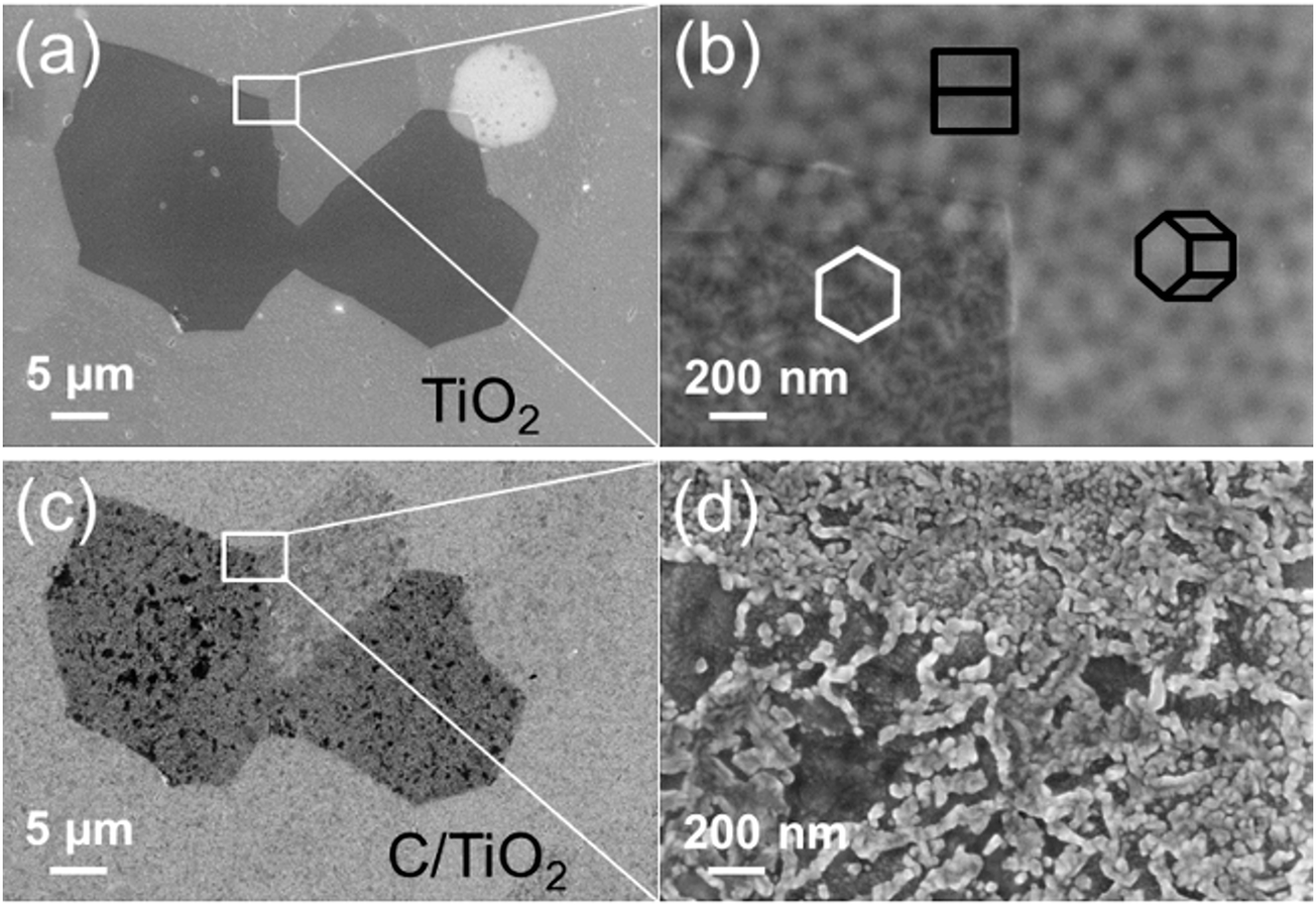 | ||
| Fig. 2 Scanning electron micrographs of a selected area on the anodic TiO2 film (a and b) and of the same area on the C/TiO2 film (c and d), with hexagonal cells representing the Ti substrate grain orientations. | ||
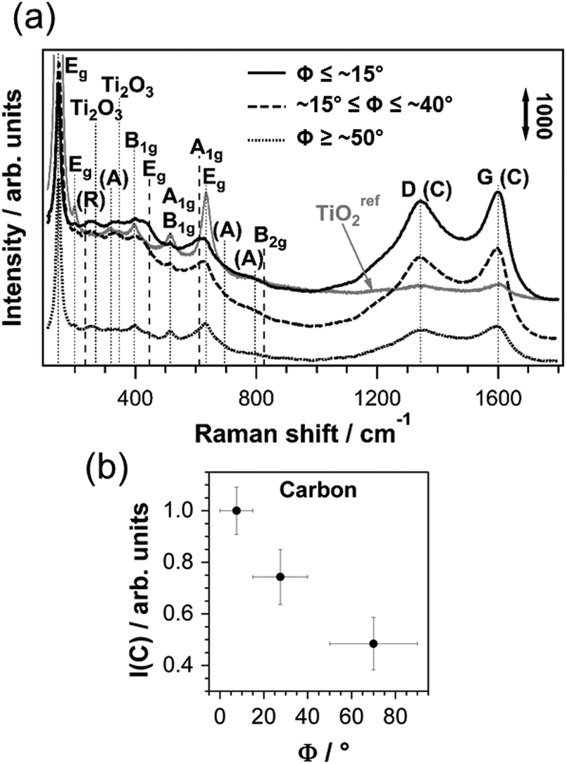 | ||
| Fig. 3 (a) Micro-Raman spectra of C/TiO2 on Tipoly for different ranges of tilt angles Φ. For clarity, the spectra are shifted vertically. TiOref2: the spectrum of the anodic TiO2 film on Ti with Φ ≤ ∼15° after thermal treatment without C2H2. Dashed lines: rutile bands, dotted lines: all other bands. D- and G-bands: from carbon (C). TiO2 combination bands: (R) = rutile, (A) = anatase. (b) Integrated peak areas of carbon bands versus Φ. Error bars of I(C): standard deviations of I(C) on grains within one Φ-range; error bars of Φ: ranges defined in Table 1. | ||
The crystalline phases and the chemical composition of the C/TiO2/Tipoly composite are determined using micro-Raman spectroscopy. The average Raman response of the film on top of single substrate grains is measured, since the focused laser beam has a lateral size of ∼5 μm, whereas the grains have a size of 10–20 μm. In the present case, the penetration depth is much larger than the C/TiO2 film thickness (see discussion in the ESI†), therefore the Raman signal originates from the entire composite film. Fig. 3 shows micro-Raman spectra of C/TiO2 for three ranges of Ti substrate tilt angles Φ. To exclude contributions of carbon contamination from secondary sources, no EBSD map was obtained for the electropolished Ti surface of this sample. All six bands of first order Raman scattering of anatase TiO2 are detected between 100 and 830 cm−1 in the C/TiO2 film.30 Due to the high proximity of the A1g band and the high frequency B1g band, they appear as one peak at ∼517 cm−1. The weak shoulders at 320 cm−1 and 695 cm−1 can be attributed to combination bands of the anatase spectrum due to second-order Raman scattering.30 The two most intense peaks of rutile, Eg and A1g, are present, as well as its most prominent combination band at ∼235 cm−1.31 Peaks found at ∼267 cm−1 and ∼347 cm−1 can be attributed to the most intense Raman signals of Ti2O3.32,33 The broad features between ∼240 and ∼395 cm−1 cannot be clearly identified. The Raman spectra reveal that the anodic TiO2 contains crystalline domains of anatase and rutile and is partially reduced after the carbothermal treatment with C2H2.
The spectra detected for different ranges of Φ clearly show that the phase composition of the film is affected by the underlying Ti substrate grain orientations. The fractions of crystalline anatase and rutile phases in the film can be deduced from the relative intensities of the corresponding Raman bands.34 A comparison between the most intense anatase B1g band (∼399 cm−1) and the rutile Eg band (∼447 cm−1), and between the rutile A1g band (∼612 cm−1) and the high frequency anatase Eg band (∼639 cm−1) indicate that there is considerably more rutile present in the thermally treated anodic TiO2 film on top of grains with Φ ≤ ∼15° than in the film on top of grains with Φ ≥ ∼50°. Grains with ∼15° ≤ Φ ≤ ∼50° exhibit mixed phase compositions.
All spectra depicted in Fig. 3 show two strong broad peaks at ∼1348 and ∼1600 cm−1 that are the characteristic D- and G-bands of carbon and can be attributed to nanocrystalline graphite (NCG).35 The ratio of the D-band intensity to the G-band intensity is determined by means of a 4-peak Gaussian fit and yields values of 0.7–0.8 independent of the substrate grain orientations (see Fig. S2 in the ESI†), which correspond to NCG clusters of approximately 6 nm diameter according to the Tuinstra–Koenig relation.35
The carbon signal intensity appears to be influenced by the substrate grain orientation. In Fig. 3 the integrated and normalized areas of the Raman signals that correspond to vibrations of carbon, I(C), are plotted versus the tilt angles Φ of the Ti substrate grains. I(C) decreases markedly with increasing substrate tilt angle; on top of substrate grains with Φ ≤ ∼15°, the intensity is about 2 times higher than on top of substrate grains with tilt angles Φ ≥ ∼50°. The Raman response of the C/TiO2 composite film differs considerably from the spectrum of a reference sample (TiOref2) that underwent the same thermal treatment without the addition of C2H2 (see Fig. 3). The intensities of the carbon bands detected on TiOref2 are much lower than the ones detected on the C/TiO2 composite, which evidences that the high amount of carbon in the latter originates from the decomposition of C2H2 and not from carbon contamination.
SPEM is performed on the C/TiO2 composite to gain complementary information about the local chemical surface composition and its dependency on the Ti substrate grain orientation. The corresponding results are summarized in Fig. 4. Cross-correlation with EBSD allows for the assignment of crystallographic orientations to the Ti substrate grains underneath the anodic TiO2 film. It is important to note that only the region at the left of the dashed line in Fig. 4b coincides with the EBSD map that was acquired on the Ti substrate, which enables the identification of possible carbon contamination generated during the EBSD measurement. The grain labeled A in Fig. 4 belongs to substrate orientations with 0°≤ Φ ≤ ∼15°, whereas the grains labelled B and C are characterized by underlying substrate tilt angles of ∼15°≤ Φ ≤ ∼40° and ∼40°≤ Φ ≤ ∼50°, respectively. Grains D and E correspond to substrate orientations with Φ ≥ ∼50° (see hexagonal cells in Fig. 4a). From Fig. 4 it can be seen that the chemical composition of the carbothermally treated film surface is considerably affected by the properties of the Ti substrate grains. In the chemical map of Fig. 4b brighter contrast corresponds to a relatively higher C 1s signal, evidencing an accordingly higher amount of carbon. In the same areas, the contrast in Fig. 4c appears darker. This can be explained by the presence of a thicker carbon layer on top of the anodic TiO2 film that attenuates the intensity of the Ti 2p core level photoelectrons. Interestingly, the film on grain C, whose underlying Ti substrate is tilted by Φ = 46°, appears to be just at the transition from high to low carbon content, since it is barely distinguishable from the surrounding area of the homogeneous shade in the chemical maps. No change in contrast can be observed across the dashed line in Fig. 4b, which proves the absence of artefacts caused by the acquisition of the EBSD map. Fig. 4d and e report the C 1s and Ti 2p3/2 spectra extracted from the indicated areas of the photoelectron micrographs. The C 1s peaks of all the studied grains are clearly dominated by the signal of graphitic carbon (sp2 hybridized carbon), detected at 284.5 eV.36 This is in accordance with the Raman response of the C/TiO2 composite, which proves the presence of NCG. The weak shoulder occurring at 285.6 eV accounts for a small fraction of diamond-like carbon (DLC, sp3 hybridized carbon).20,36 No defined peak of carbidic carbon (C–Ti bonds) is found at 281.7 eV (see Fig. S3 in the ESI†), hence only a negligible amount of this species is present at the C/TiO2 interface. For all studied grains, the Ti 2p3/2 region is dominated by the TiO2 peak at 459 eV20 that originates from the anodic film. The small shoulder at the low binding energy tail of the peak reveals the presence of reduced titania species, such as Ti(III) in Ti2O3 at 457 eV,20 which confirms the Raman results. In accordance with the C 1s spectrum, no pronounced TiC (or TiO) component is detected at 454.9 eV in the Ti 2p spectrum (see Fig. S3 in ESI†). Fig. 4f shows the variation of the integrated and normalized carbon signal intensities I(C), extracted from the C 1s photoelectron micrograph, with substrate grain orientation, which gives an estimate of the differences in carbon content. As already indicated by the contrast in the chemical maps, there is an abrupt drop in the carbon intensity from grains with small tilt angles Φ (A, B) to grains with high tilt angles Φ (D, E) and a transition between these two types of substrate grains represented by grain C. The carbon signal intensity of grain A is about 1.7 times higher than the one of grain D. This trend is consistent with the Raman results (Fig. 3b). The complementary contrast in the chemical maps confirms a layered structure of the C/TiO2 composite with a carbon film on top of the anodic TiO2.
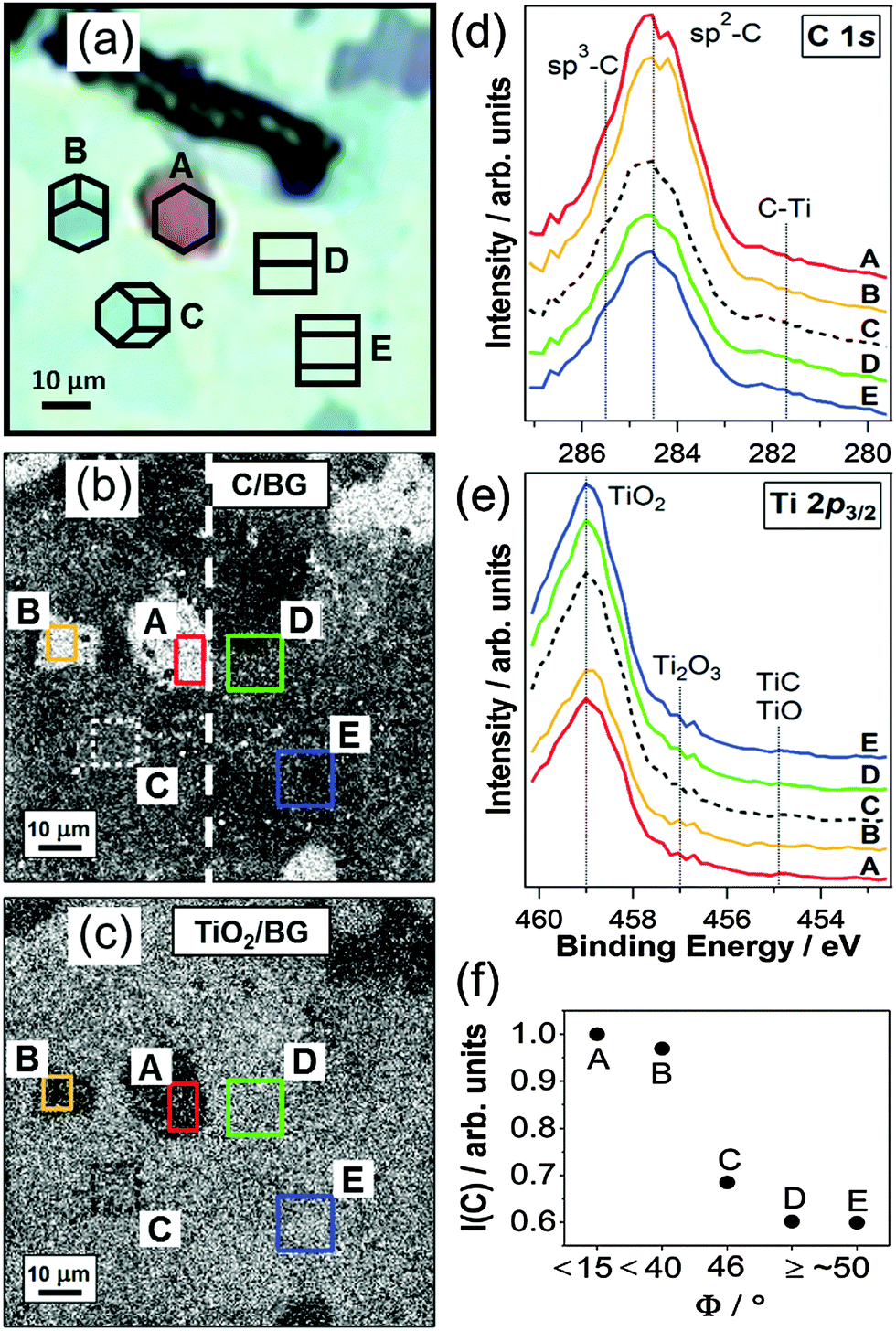 | ||
| Fig. 4 (a) Optical micrograph of the anodic TiO2 film with surface projected hexagonal cells representing Ti substrate grain orientations (A–E). Chemical maps of the C 1s (b) and Ti 2p3/2 (c) core levels obtained for the same film by SPEM after thermal treatment with C2H2 at 550 °C. Spectra extracted from the boxes in the C 1s (d) and the Ti 2p3/2 (e) chemical maps. For clarity, the spectra are shifted vertically. (f) Integrated C 1s signal intensities, derived from (d), versus tilt angle Φ of Ti substrate grains. | ||
In contrast, carbothermal treatment of anodic TiO2 films carried out in UHV and with different carbon precursors are reported to yield a conversion to TiO and TiC after shorter annealing times and lower temperatures.20,36 However, such TiOxCy compact films were found to suffer from partial re-oxidation to TiO2 accompanied by the formation of graphitic carbon at the surface when exposed to ambient air. This was rationalized by DFT calculations which revealed that an increasing oxygen partial pressure favors the phase separation into graphitic carbon on top of anatase TiO2.20 In the present study, the anodic films are treated with acetylene in a flow reactor with the supporting gas argon, which involves higher oxygen partial pressures than under UHV conditions. Thus it is likely that these conditions hinder the formation of TiOxCy at 550 °C in favor of effective deposition of a carbon layer, or that only a low fraction of TiC and TiO species forms, which are easily re-oxidized upon exposure to air.
Since SPEM yields a photoelectron signal of TiO2 on all substrate grains, the maximum carbon layer thickness can be estimated from the probing depth for atomically planar graphitic carbon, which yields a thickness of about 2.3 nm. A close look at the chemical maps reveals that the film on top of individual substrate grains has no perfectly homogeneous composition (see black spots on grain A in Fig. 4b), which is supported by the inhomogeneous coverage of the deposited film that is observed by SEM (Fig. 2d). This finding is most likely related to the properties of the anodic TiO2 at the moment that C2H2 interacts with it during the carbothermal treatment, which is described in the next section.
3.3 Thermal treatment without C2H2
During carbothermal treatment, C2H2 is added to the process after one hour of annealing at 550 °C under an argon gas flow. It can be expected that prior to the addition of C2H2, the properties of the anodic TiO2 film, in particular its crystallinity, are different from those of the pristine film and that these properties affect the interaction with C2H2. Hence, the investigation of the substrate grain dependent properties of the anodic TiO2 film prior to the addition of C2H2 may unravel the origin of the grain dependent chemical composition of the final C/TiO2/Tipoly composite. For this purpose, a reference sample (TiOref2) was prepared under the same conditions as the C/TiO2 composite, but the annealing treatment was stopped prior to the introduction of C2H2. An EBSD map of the polycrystalline Ti substrate recorded after electropolishing allows a precise identification of the tilt angles Φ of the grains.Fig. 5a shows the Raman response of the TiOref2 film on individual substrate grains that exhibit different tilt angles Φ. The colors of the spectra correspond to the substrate grain orientations that are indicated by black spots in the standard triangle (the studied grains are depicted in Fig. 1). Along the arrows, the tilt angle Φ of the substrate grains varies from 0° to 90°. In all spectra the characteristic bands of first-order Raman scattering of crystalline anatase TiO2 are detected. The weak peaks at 320 cm−1 and 796 cm−1 are combination bands of anatase.30 Apart from a weak feature around ∼235 cm−1, no distinct peaks in the spectrum can be attributed to rutile, which suggests a very low fraction of this phase in the TiOref2 film. All spectra show two peaks at ∼1340 and ∼1600 cm−1 that are the characteristic D- and G-bands of carbon, which indicate the presence of NGC.35
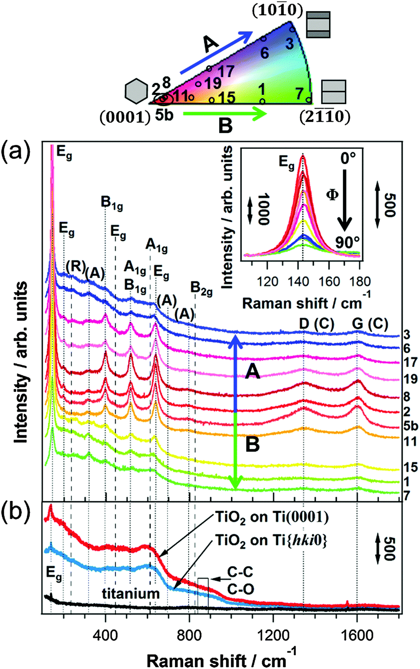 | ||
| Fig. 5 (a) Micro-Raman spectra of TiOref2. For clarity the spectra are shifted vertically. Dashed lines: rutile, dotted lines: anatase, carbon. D- and G-bands: carbon (C). TiO2 combination bands: rutile (R), anatase (A). Inset: anatase Eg peak (143 cm−1) evolution with tilt angle. Arrows (A and B): directions of Φ variation from 0° to 90°. (b) Micro-Raman spectrum of electropolished Ti (black) and an anodic TiO2 film on ∼Ti(0001) (red) and ∼Ti{hki0} (blue). | ||
Fig. 5b shows the spectra of an anodic TiO2 film on top of two different Ti substrate grains with Φ ≥ ∼50° (i.e. grains belonging to the group of ∼Ti{hki0} orientations – see Table 1) and Φ ≤ ∼15° (i.e. ∼Ti(0001)). Apart from the weakly protruding Eg peak of anatase TiO2 at 143 cm−1, both Raman spectra are characterized by very broad and undefined features below ∼1000 cm−1, evidencing that the film is mainly amorphous.37–39 The intensity of the Raman signal of the TiO2 film on ∼Ti(0001) is slightly higher than that of the film on ∼Ti{hki0}, which indicates that the grain orientation of the Ti substrate influences the properties of the pristine anodic TiO2 film on top. The comparison between the Raman response of the TiOref2 system and the pristine anodic TiO2 film discloses the changes that have occurred upon annealing: the thermal treatment at 550 °C leads to the crystallization of the anodic TiO2 film. No graphitic carbon is detected on the pristine anodic TiO2. The signal between 840 and 890 cm−1, however, could be assigned to the Raman active C–C and C–O stretching of organic carbon contamination.38–43 The carbon detected on TiOref2 may therefore originate from organic contamination adsorbed onto the surface of anodic TiO2 and converted to graphitic carbon during the thermal treatment. An electropolished titanium substrate yields a flat baseline signal with almost no features (black spectrum in Fig. 5b). Only at around 143 cm−1 a small peak is detected which can be attributed to the corresponding Eg band of anatase TiO2, arising most likely from the natural oxide film that is usually present on titanium. There is another small feature at about 1555 cm−1, which might originate from carbon contamination as well and which is also present on the anodic TiO2 film.
A strong influence of the substrate grain orientation on the Raman response of TiOref2 is found. While the anatase bands that are detected on top of grains with Φ ≤ ∼15° (red spectra in Fig. 5a) are relatively intense and sharp, the same peaks are not only weaker and broader when detected on grains with Φ ≥ ∼50° (green and blue spectra in Fig. 5a), but also embedded in a plateau-like background signal, which can be attributed to a considerable fraction of amorphous TiO2 in these films. Well-defined, intense Raman bands of narrow full width at half maximum (FWHM) are characteristic of an extended single crystal (see Fig. S4 in the ESI†)30,44 and are hence an indication of high crystallinity of the detected anatase phase. The more intense the characteristic bands of anatase are, the higher is the fraction of this crystalline phase in the probed volume of TiOref2. Peaks of small FWHM indicate a high long-range order and thus sufficiently large crystalline domains. The features of the amorphous TiO2 background are also present, but less pronounced, on grains with intermediate tilt angles, ∼15° ≤ Φ ≤ ∼50° (orange, yellow, light and dark purple spectra in Fig. 4a), suggesting that the anodic TiO2 film is partially crystalline on these grains. The crystallinity of the anatase phase gradually improves with decreasing Φ, as can be inferred from the evolution of the Eg band at 143 cm−1 (inset in Fig. 5a). A close comparison between the Raman spectra of grains 8, 2 and 5b (red in Fig. 5a) reveals a variation in relative peak heights of the three characteristic anatase bands detected between 350 and 650 cm−1. This can be attributed to different preferential orientations of the anatase crystallites on these grains and is not related to varying crystallinity (see Fig. S4 and S5 and the discussion in the ESI†).
Together with the improvement of crystallinity in the TiOref2 film, an increase in the intensity of the characteristic D- and G-bands of NCG is observed with decreasing Φ. This suggests that the amount of produced graphitic carbon depends on the crystallinity of anodic TiO2, and in particular on its anatase content.
For a detailed analysis of the dependency of the TiO2 crystallinity and the carbon content on the substrate tilt angle, the low frequency Eg (∼143 cm−1), the B1g (∼396 cm−1) and the high frequency Eg (∼639 cm−1) bands of anatase, as well as the Raman signal of carbon are fitted using Lorentzian and Gaussian line shapes (see Fig. S6 in the ESI†). The fractions of the crystalline TiO2, the overall (i.e. crystalline and amorphous) TiO2 and the overall carbon phase in the film are then proportional to the integrated areas (i.e. intensities I) of the corresponding Raman signals (see ESI†). To eliminate the possible effects of surface roughness of the TiOref2 film on the quantity of generated NCG, the carbon signal intensities are corrected for the topographic surface area (Ispec(C)), which was determined by AFM (see Fig. S7 in the ESI†). The obtained results are reported in Fig. 6.
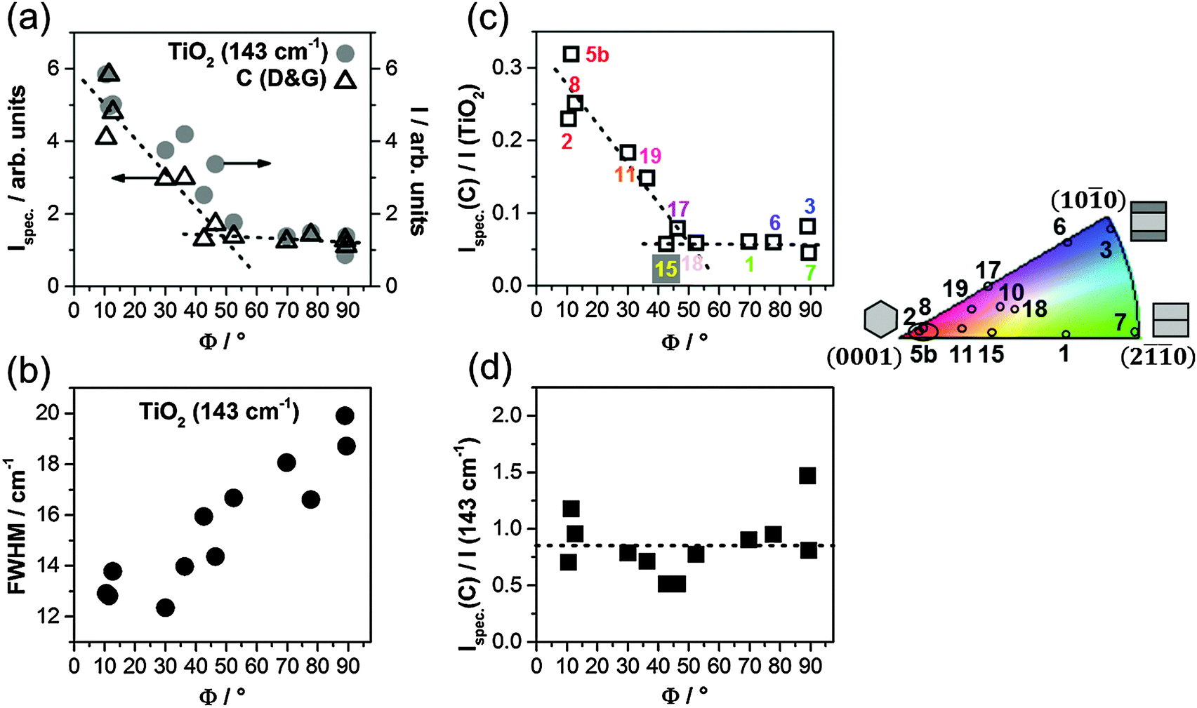 | ||
| Fig. 6 Evaluation of Raman spectra of TiOref2 as a function of the substrate tilt angle Φ. The studied grains are labeled with numbers and marked in the standard triangle. (a) Anatase Eg band intensities at ∼143 cm−1 and area-specific carbon signal intensities (Ispec(C)); (b) FWHM of the anatase Eg band at ∼143 cm−1. (c) The ratio of Ispec(C) and the overall Raman response of crystalline and amorphous TiO2 (I(TiO2)). (d) The ratio of Ispec(C) and the intensity of the anatase Eg band at ∼143 cm−1. Dashed lines in (a) and (c): linear least squares fits of carbon band intensities below 55° and above 40°. Dashed line in (d): arithmetic mean (0.85 ± 0.27). | ||
The overall fraction of crystalline anatase stays almost constant and low for Φ ≥ ∼50° and abruptly increases below Φ ∼ 50° to five times higher values (Fig. 6a). The intensities of the B1g (∼396 cm−1) and the high frequency Eg bands (∼639 cm−1) of anatase follow the same trends (see Fig. S8a in the ESI†). In addition, a progressive blue-shift of the B1g band from ∼397 to ∼402 cm−1 and a parallel red-shift of the Eg band from ∼637 to ∼628 cm−1 are observed when the tilt angle Φ increases from 0° to 90°, which can be attributed to an increasing fraction of amorphous TiO2 (see Fig. S8b and c in the ESI†).
The FWHM of the anatase Eg band (∼143 cm−1) drops linearly with decreasing Φ (Fig. 6b). For anatase TiO2 nanocrystals, the FWHM of the Eg band was reported to be inversely related to their dimensions.44–46 Hence, this trend indicates a continuous increase of the size of the crystalline anatase domains with decreasing Φ. However, the smallest FWHM value of about 12 cm−1 is still higher than the value of 7 cm−1 that is expected for bulk anatase TiO2 (see Fig. S4 in the ESI†).44,47 Therefore, the thermally treated anodic TiO2 film can be considered polycrystalline on top of every single substrate grain. Similar FWHM values were obtained for anatase TiO2 nanoparticles with a crystallite size of less than ∼20 nm,46 thus the domain sizes for thermally treated anodic TiO2 are in the nanometer range.
The area-specific carbon signal intensities, Ispec(C), give a qualitative measure of the amount of carbon on the thermally treated anodic film. From Fig. 6a it can be seen that Ispec(C) follows the same trend with the substrate tilt angle as the intensity of the anatase Eg band. In Fig. 6c, Ispec(C) is divided by the overall Raman response of TiO2, I(TiO2), (including the amorphous phase) on individual substrate grains. As in Fig. 6a, two regions of different slopes can be identified and the crossing of the corresponding least squares linear fits (dashed lines) yields the tilt angle Φ ∼ 50° as a threshold value. Below this point, Ispec(C)/I(TiO2) and therewith the amount of NCG that is produced on the TiOref2 upon thermal treatment is increased substantially. When Ispec(C) is only divided by the intensity of the anatase Eg band (143 cm−1), a plot versus Φ yields an almost constant line (Fig. 6d). This evidences that the two quantities, i.e. the amount of NCG and crystalline TiO2, are closely linked. The intensity ratio of the carbon bands is determined to be 0.7–0.8, independent of the crystallographic orientations of the substrate grains underneath the film, which corresponds to NCG clusters of approximately 6 nm on the overall film (see ESI†).
4. Discussion
4.1 Crystallinity of the anodic film
The phase evolution of anodic titania films during isothermal annealing proceeds from initially amorphous TiO2 to phase-pure anatase, over mixed phases of anatase and rutile towards phase pure rutile TiO2, where the final phase composition depends on the annealing temperature, atmosphere and duration.38,39,48 A variation of the tilt angle Φ of the substrate grains from ∼50° to 0° appears to have the same effect on the final crystallinity of TiOref2 as an enhancement of annealing temperature. This implies that the substrate grain orientation, and in particular the tilt angle Φ, has a strong impact on the kinetics of the phase transition. From the literature it is known that the compact anodic TiO2 on top of ∼Ti(0001) is thinner than on ∼Ti{hki0} and contains higher donor concentrations, i.e. oxygen vacancies.26,49,50 This is likely to affect the atomic reorganization or diffusion processes during annealing and therewith yield a higher isothermal crystallization rate for TiO2 on ∼Ti(0001) than for TiO2 on ∼Ti{hki0}. In particular, a considerable increase of donor density, supported by a parallel increase in the electron transfer rate, oxygen evolution current and photocurrent, has been found for anodic TiO2 films on top of Ti substrate grains with tilt angles decreasing below Φ ∼ 45°,25,28 which is in very good agreement with the observed increase of TiO2 crystallinity for tilt angles Φ ≤ ∼50° (see Fig. 6a).The difference in phase composition of TiOref2 and C/TiO2 is related to the annealing time, which is longer for the thermal treatment with C2H2, hence yielding a considerable fraction of rutile TiO2; in addition, the carbon present on the TiO2 may have an effect on the crystallization kinetics.51,52
4.2 Carbon content in the C/TiO2 composite
SPEM, micro-Raman spectroscopy and SEM evidence that carbothermal treatment of a compact anodic TiO2 film with C2H2 at 550 °C yields a C/TiO2 composite material, consisting of a few nm thick nanocrystalline graphitic carbon film on top of slightly reduced, polycrystalline TiO2. On the reference sample TiOref2, which is thermally treated without C2H2, a significantly less amount of carbon is detected, which originates from organic or hydrocarbon contamination of the anodic TiO2 only.The carbon signal intensity, extracted from SPEM and micro-Raman spectroscopy, follows a very similar trend with Φ for both TiOref2 and C/TiO2. There are mainly two classes of grains: class one comprises substrate grains with tilt angles of 0° ≤ Φ ≤ ∼40° where a relatively high amount of carbon is deposited on the oxide film; class two covers all grains with tilt angles Φ ≥ ∼50° that exhibit a relatively low fraction of carbon after the carbothermal treatment of the anodic TiO2. Grains with ∼40° ≤ Φ ≤ ∼50° belong to a transition zone, where an orientation of Φ ∼ 50° can be identified as a threshold value.
The nature of the carbon film found on TiOref2 and C/TiO2 is very similar, as evidenced by the resembling shapes of the Raman responses of carbon: the evaluation of the carbon bands' intensity ratios yields a NCG cluster size of approximately 6 nm, independent of the substrate grain orientation and the carbon source.
The formation of a grain-dependent carbon layer under the applied carbothermal treatment strongly suggests that C2H2 (and even organic contamination) is not thermally but catalytically decomposed at the surface of TiO2.53 Furthermore, the presented results evidence that crystalline TiO2, in particular the anatase phase, is able to decompose C2H2, since only a small amount of carbon is found on TiO2 that is mainly amorphous. It has been reported that Ti4+–O2− Lewis acid–base pairs on the surface of crystalline TiO2 are the active centers for a heterolytic dissociation of C2H2 initiating self-assembly processes of acetylene to form polycyclic aromatic hydrocarbons at room temperature and graphitic carbon at sufficiently high temperatures (650 °C in ref. 53).54,55 Anatase TiO2 was found to be particularly efficient for the decomposition of acetylene, which is in line with our findings.
The crystallinity of compact anodic films on polycrystalline Ti substrates is affected by the Ti substrate grain orientations. This causes the observed grain dependent average chemical surface composition of the obtained C/TiO2 composite. In a previous in situ study on the conversion of anodic TiO2/Tipoly into TiOxCy/Tipoly under UHV conditions, a substrate grain dependent chemical composition of the final TiOxCy film was found, evidencing that also under different synthesis conditions (temperature, pressure, and carbon source), effects of the polycrystalline substrate need to be taken into account.20 A detailed investigation of the temperature-dependence of the surface chemistry and the structure of this system is ongoing and will be published separately.
From the FWHM values of the anatase Eg (143 cm−1) bands it is deduced that the TiOref2 film consists of polycrystalline anatase with nanometer size crystallites. This may explain why only nanocrystalline and no extended graphitic carbon layers are formed in the course of the thermal treatment. Furthermore, it gives an explanation for the inhomogeneous carbon coverage of TiO2 on individual substrate grains as observed with SPEM and SEM, which is particularly emphasized on top of grains that are tilted by Φ ≤ ∼15°: a polycrystalline TiO2 film consists of anatase domains that have different orientations exposing different faces at the surface, which in turn affects their activity towards C2H2 decomposition. The reason for this is that different anatase faces exhibit different fractions of active Ti4+–O2− centers. According to the literature a high fraction of these sites appears to be present on dehydroxylated, stoichiometric and extended (001) and/or (010) planes of crystalline anatase.55,56
Our results demonstrate that the peculiar properties of compact anodic TiO2 films on Tipoly have an important impact on the synthesis of C/TiO2/Tipoly composites via the carbothermal route. The obtained substrate grain dependent chemical composition and structure of the film is likely to affect its overall performance when applied in electrocatalysis or Li-ion battery studies. For example, it is known that local variations in the charge transfer kinetics play a crucial role in the overall activity of electrocatalysts.57 The grain dependent electrochemical stability of Pt/TiOxCy found in ref. 16 is another consequence of these properties of anodic TiO2 on Tipoly. An adapted design of C/TiO2 films requires a detailed knowledge of the substrate texture and a controlled crystallization of the anodic film during the carbothermal treatment. The presence of crystalline anatase TiO2 required for the reactive decomposition of C2H2 at 550 °C and atmospheric pressure has implications on the carbothermal synthesis of functional C/TiO2 materials in general.
5. Conclusions
In the present work the substrate grain dependent properties of planar C/TiO2/Tipoly composite films that are synthesized via carbothermal treatment of compact anodic TiO2 with C2H2 in a flow reactor at 550 °C have been investigated. A pronounced correlation between the amount of deposited carbon and the Ti substrate grain orientations is observed: a significantly high amount of graphitic carbon is deposited on the anodic TiO2 film on top of ∼Ti(0001) grains than on TiO2 on top of ∼Ti{hki0} grains. The origin of the grain effect is identified as a substrate grain-dependent crystallization of the initially amorphous anodic TiO2 film to nanocrystalline anatase during the thermal treatment, which in turn affects the activity of TiO2 towards C2H2 decomposition to form nanocrystalline graphite. This effect emphasizes the importance of TiO2 precursor crystallinity for the synthesis of C/TiO2 functional materials via a carbothermal route. In the case of anodic TiO2 films, the crystallization needs to be guided towards extended single crystalline anatase domains exposing their most active facets to enable the deposition of extended graphite layers, which, in combination with the possibility of nanostructuring anodic TiO2, provides a highly interesting functional material. Indeed, nanotubular C/TiO2−x composite layers, synthesized via the carbothermal route, have shown promising Li storage capacities,15 which may be further improved by means of an optimized synthesis, taking into account the crystallization characteristics of anodic films.A detailed knowledge of local physico-chemical properties, as-obtained in this study, is important to understand the overall performance of functional materials. In view of the potential applications of C/TiO2 composite materials in energy conversion and storage, the herein introduced planar C/TiO2/Tipoly composite is proposed as a model system for the investigation of property–performance relationships. Taking advantage of the substrate grain effect, two-dimensional property maps of the C/TiO2 film that correlate (substrate grain dependent) intrinsic physico-chemical properties, such as chemical composition or morphology, and functional properties, such as electric conductivity, catalytic activity or (electro-)chemical stability, will give valuable information about the material. This can be realized by means of local analysis tools, such as SPEM21 and micro-electrochemistry.58
Author contributions
The manuscript was written through contributions of all authors. CR planned and executed or coordinated the experiments, evaluated the data and drafted the manuscript. MF participated in the SPEM experiments and contributed to the SPEM data evaluation. CVV and LC participated in the SPEM experiments. NB evaluated the EBSD measurements which were performed by SJ. CH performed the Raman measurements. LG and MA gave technical support at the ESCAmicroscopy beamline of the Elettra Synchrotron in Trieste. SA conceived of the SPEM study and gave advice for the data evaluation. GG gave general advisory support. JKL supervised the study and actively participated in drafting the manuscript.All authors have given approval to the final version of the manuscript.
Funding sources
The research of the manuscript was supported by funds of the EU RTD Framework Programme FP7 (FP7-NMP-2012-SMALL-6, project title DECORE, project number 309741).Conflicts of interest
The authors declare no competing financial interest.Abbreviations
| UHV | Ultra-high vacuum |
| EBSD | Electron backscatter diffraction |
| AFM | Atomic force microscopy |
| SEM | Scanning electron microscopy |
| SPEM | Scanning photoelectron microscopy |
| FWHM | Full width at half maximum |
| NCG | Nanocrystalline graphite |
Acknowledgements
The authors thank the EU RTD Framework Programme FP7 (FP7-NMP-2012-SMALL-6, project title DECORE, project number 309741) for financial support. We thank the DFG for financial support during the early stages of this study (project KU2398/1-1). Furthermore, the chair of Technical Chemistry II at TU München is acknowledged for the possibility for preliminary Raman studies, especially we are grateful to Jennifer Hein and Prof. Andreas Jentys for their assistance. We thank Prof. Kurt Hingerl for measuring the thickness of the anodic TiO2. We thank Dr Katrin F. Domke for the helpful discussions on the evaluation of Raman data.References
- L. Xiong and A. Manthiram, Electrochim. Acta, 2004, 49, 4163 CrossRef CAS.
- J. Tian, G. Sun, M. Cai, Q. Mao and Q. Xin, J. Electrochem. Soc., 2008, 155, B187 CrossRef CAS.
- P. V. Kamat, J. Phys. Chem. Lett., 2010, 1, 520 CrossRef CAS.
- T. Fröschl, U. Hörmann, P. Kubiak, G. Kučerová, M. Pfanzelt, C. K. Weiss, R. J. Behm, N. Hüsing, U. Kaiser, K. Landfester and M. Wohlfahrt-Mehrens, Chem. Soc. Rev., 2012, 41, 5313 RSC.
- M. Dahl, Y. Liu and Y. Yin, Chem. Rev., 2014, 114, 9853 CrossRef CAS PubMed.
- W. Fan, Q. Lai, Q. Zhang and Y. Wang, J. Phys. Chem. C, 2011, 115, 10694 CAS.
- B. Tryba, A. W. Morawski, T. Tsumura, M. Toyoda and M. Inagaki, J. Photochem. Photobiol., A, 2004, 167, 127 CrossRef CAS.
- Y. Zhang, Z.-R. Tang, X. Fu and Y.-J. Xu, ACS Nano, 2010, 4, 7303 CrossRef CAS PubMed.
- Y. T. Liang, B. K. Vijayan, O. Lyandres, K. A. Gray and M. C. Hersam, J. Phys. Chem. Lett., 2012, 3, 1760 CrossRef CAS PubMed.
- M. Favaro, S. Agnoli, C. Di Valentin, C. Mattevi, M. Cattelan, L. Artiglia, E. Magnano, F. Bondino, S. Nappini and G. Granozzi, Carbon, 2014, 68, 319 CrossRef CAS.
- A. Zana, C. Rüdiger, J. Kunze-Liebhäuser, G. Granozzi, N. E. A. Reeler, T. Vosch, J. J. K. Kirkensgaard and M. Arenz, Electrochim. Acta, 2014, 139, 21 CrossRef CAS.
- R. Hahn, F. Schmidt-Stein, J. Salonen, S. Thiemann, Y. Song, J. Kunze, V.-P. Lehto and P. Schmuki, Angew. Chem., Int. Ed., 2009, 48, 7236 CrossRef CAS PubMed.
- Y. Kado, R. Hahn and P. Schmuki, J. Electroanal. Chem., 2011, 662, 25 CrossRef CAS.
- C. Rüdiger, F. Maglia, S. Leonardi, M. Sachsenhauser, I. D. Sharp, O. Paschos and J. Kunze, Electrochim. Acta, 2012, 71, 1 CrossRef.
- J. Brumbarov, J. P. Vivek, S. Leonardi, C. Valero-Vidal, E. Portenkirchner and J. Kunze-Liebhäuser, J. Mater. Chem. A, 2015, 3, 16469 CAS.
- C. Rüdiger, J. Brumbarov, F. Wiesinger, S. Leonardi, O. Paschos, C. Valero Vidal and J. Kunze-Liebhäuser, ChemCatChem, 2013, 5, 3219 CrossRef.
- L. Calvillo, G. García, A. Paduano, O. Guillén-Villafuerte, C. Valero-Vidal, A. Vittadini, M. Bellini, A. Lavacchi, S. Agnoli, A. Martucci, J. Kunze-Liebhäuser, E. Pastor and G. Granozzi, ACS Appl. Mater. Interfaces, 2016, 8, 716 CAS.
- A. Aladjem, J. Mater. Sci., 1973, 8, 688 CrossRef CAS.
- P. Roy, S. Berger and P. Schmuki, Angew. Chem., Int. Ed., 2011, 50, 2904 CrossRef CAS PubMed.
- L. Calvillo, D. Fittipaldi, C. Rüdiger, S. Agnoli, M. Favaro, C. Valero-Vidal, C. Di Valentin, A. Vittadini, N. Bozzolo, S. Jacomet, L. Gregoratti, J. Kunze-Liebhäuser, G. Pacchioni and G. Granozzi, J. Phys. Chem. C, 2014, 118, 22601 CAS.
- M. K. Abyaneh, L. Gregoratti, M. Amati, M. Dalmiglio and M. Kiskinova, e-J. Surf. Sci. Nanotechnol., 2011, 9, 158 CrossRef.
- L. Gregoratti, A. Barinov, E. Benfatto, G. Cautero, C. Fava, P. Lacovig, D. Lonza, M. Kiskinova, R. Tommasini, S. Mähl and W. Heichler, Rev. Sci. Instrum., 2004, 75, 64 CrossRef CAS.
- H.-J. Bunge, Texture Analysis in Materials Science: Mathematical Methods, Butterworths & Co, London, U.K., 2nd edn, 1982 Search PubMed.
- The lattice cell was drawn with the software Diamond 4.0 (demonstration version).
- U. König and B. Davepon, Electrochim. Acta, 2001, 47, 149 CrossRef.
- M. V. Diamanti, M. P. Pedeferri and C. A. Schuh, Metall. Mater. Trans. A, 2008, 39, 2143 CrossRef.
- A. K. Sharma, Thin Solid Films, 1992, 208, 48 CrossRef CAS.
- S. Kudelka and J. W. Schultze, Electrochim. Acta, 1997, 42, 2817 CrossRef CAS.
- J. W. Schultze, B. Davepon, F. Karman, C. Rosenkranz, A. Schreiber and O. Voigt, Corros. Eng., Sci. Technol., 2004, 39, 45 CrossRef CAS.
- T. Ohsaka, F. Izumi and Y. Fujiki, J. Raman Spectrosc., 1978, 7, 321 CrossRef.
- S. P. S. Porto, P. A. Fleury and T. C. Damen, Phys. Rev., 1967, 154, 522 CrossRef CAS.
- A. Mooradian and P. M. Raccah, Phys. Rev. B: Solid State, 1971, 3, 4253 CrossRef.
- S.-W. Hsu, T.-S. Yang, T.-K. Chen and M.-S. Wong, Thin Solid Films, 2007, 515, 3521 CrossRef CAS.
- J. Zhang, M. Li, Z. Feng, J. Chen and C. Li, J. Phys. Chem. B, 2006, 110, 927 CrossRef CAS PubMed.
- A. C. Ferrari and J. Robertson, Phys. Rev. B: Condens. Matter Mater. Phys., 2000, 61, 95 CrossRef.
- M. Favaro, S. Leonardi, C. Valero-Vidal, S. Nappini, M. Hanzlik, S. Agnoli, J. Kunze-Liebhäuser and G. Granozzi, Adv. Mater. Interfaces, 2015, 2, 1400462 Search PubMed.
- M. Fernández-García, X. Wang, C. Belver, J. C. Hanson and J. A. Rodriguez, J. Phys. Chem. C, 2007, 111, 674 Search PubMed.
- V. Likodimos, T. Stergiopoulos, P. Falaras, J. Kunze and P. Schmuki, J. Phys. Chem. C, 2008, 112, 12687 CAS.
- F. D. Hardcastle, H. Ishihara, R. Sharma and A. S. Biris, J. Mater. Chem., 2011, 21, 6337 RSC.
- H. Matsuura, M. Hiraishi and T. Miyazawa, Spectrochim. Acta, 1972, 2, 2299 CrossRef.
- J. F. Mammone and S. K. Sharma, J. Phys. Chem., 1980, 84, 3130 CrossRef CAS.
- N. Ito, T. Fujiyama and Y. Udagawa, Bull. Chem. Soc. Jpn., 1983, 56, 379 CrossRef CAS.
- I. H. Boyaci, H. E. Genis, B. Guven, U. Tamer and N. Alper, J. Raman Spectrosc., 2012, 43, 1171 CrossRef CAS.
- D. Bersani, P. P. Lottici and X.-Z. Ding, Appl. Phys. Lett., 1998, 72, 73 CrossRef CAS.
- W. F. Zhang, Y. L. He, M. S. Zhang, Z. Yin and Q. Chen, J. Phys. D: Appl. Phys., 2000, 33, 912 CrossRef CAS.
- A. Li Bassi, D. Cattaneo, V. Russo, C. E. Bottani, E. Barborini, T. Mazza, P. Piseri, P. Milani, F. O. Ernst, K. Wegner and S. E. Pratsinis, J. Appl. Phys., 2005, 98, 1 CrossRef.
- T. Ohsaka, J. Phys. Soc. Jpn., 1980, 48, 1661 CrossRef CAS.
- D. Regonini, A. Jaroenworaluck, R. Stevens and C. R. Bowen, Surf. Interface Anal., 2010, 42, 139 CrossRef CAS.
- B. Davepon, J. W. Schultze, U. König and C. Rosenkranz, Surf. Coat. Technol., 2003, 169–170, 85 CrossRef CAS.
- S. Kudelka, A. Michaelis and J. W. Schultze, Electrochim. Acta, 1996, 41, 863 CrossRef CAS.
- T. Tsumura, N. Kojitani, I. Izumi, N. Iwashita, M. Toyoda and M. Inagaki, J. Mater. Chem., 2002, 12, 1391 RSC.
- M. Pfanzelt, P. Kubiak, U. Hörmann, U. Kaiser and M. Wohlfahrt-Mehrens, Ionics, 2009, 15, 657 CrossRef CAS.
- I. Eswaramoorthi and L.-P. Hwang, Diamond Relat. Mater., 2007, 16, 1571 CrossRef CAS.
- S. M. Jain, J. J. Biedrzycki, V. Maurino, A. Zecchina, L. Mino and G. Spoto, J. Mater. Chem. A, 2014, 2, 12247 CAS.
- J. J. Biedrzycki, S. Livraghi, I. Corazzari, L. Mino, G. Spoto and E. Giamello, Langmuir, 2015, 31, 569 CrossRef CAS PubMed.
- G. Martra, Appl. Catal., A, 2000, 200, 275 CrossRef CAS.
- A. N. Patel, M. G. Collignon, M. A. O'Connell, W. O. Y. Hung, K. McKelvey, J. V. MacPherson and P. R. Unwin, J. Am. Chem. Soc., 2012, 134, 20117 CrossRef CAS PubMed.
- S. O. Klemm, J.-C. Schauer, B. Schuhmacher and A. W. Hassel, Electrochim. Acta, 2011, 56, 4315 CrossRef CAS.
Footnotes |
| † Electronic supplementary information (ESI) available: Additional details on experimental methods. Optical appearance of TiOref2 and C/TiO2. Additional Raman measurements of TiOref2 and C/TiO2, evaluation of Raman spectra, and additional Raman analysis. Raman spectra of oriented anatase single crystals. SPEM results of a reference sample with TiC/TiO species. Roughness analysis of TiOref2 by AFM. See DOI: 10.1039/c5cp07727c |
| ‡ Present address: Institut für Physikalische Chemie, Leopold-Franzens-Universität Innsbruck, Innrain 52c, 6020 Innsbruck, Austria. |
| § Present address: Advanced Light Source (ALS) and Joint Center for Artificial Photosynthesis (JCAP), Lawrence Berkeley National Laboratory, 1 Cyclotron Rd., Berkeley, CA 94720, USA. |
| ¶ Present address: Advanced Light Source (ALS) and Joint Center for Energy Storage Research (JCESR), Lawrence Berkeley National Laboratory, 1 Cyclotron Rd., Berkeley, CA 94720, USA. |
| This journal is © the Owner Societies 2016 |