
 Open Access Article
 This Open Access Article is licensed under a
 Creative Commons Attribution 3.0 Unported Licence
A mechanism of Cu work function reduction in CsBr/Cu photocathodes
M. T. E.
Halliday
*a,
W. P.
Hess
b and
A. L.
Shluger
a
aDepartment of Physics and Astronomy and the London Centre for Nanotechnology, University College London, Gower Street, London WC1E 6BT, UK. E-mail: a.shluger@ucl.ac.uk
bPhysical Sciences Division, Pacific Northwest National Laboratory, P.O. Box 999, Richland, WA 99352, USA
First published on 15th February 2016
Abstract
Thin films of CsBr deposited on Cu(100) have been proposed as next-generation photocathode materials for applications in particle accelerators and free-electron lasers. However, the mechanisms underlying an improved photocathode performance as well as their long-term stability remain poorly understood. We present Density Functional Theory (DFT) calculations of the work function reduction following the application of CsBr thin film coatings to Cu photocathodes. The effects of both flat and rough interface and van der Waals forces are examined. Calculations suggest that CsBr films can reduce the Cu(100) work function by about 1.5 eV, which would explain the observed increase in quantum efficiency (QE) of coated vs. uncoated photocathodes. A model explaining the experimentally observed laser activation of photocathodes is provided whereby the photo-induced creation of Br vacancies and Cs–Br di-vacancies and their subsequent diffusion to the Cu/CsBr interface lead to a further increase in QE after a period of laser irradiation.
1 Introduction
Free-electron laser X-ray light sources (XFELs) require electron injectors with a high repetition rate, high brightness, low emittance and long lifetime. Their development is a key challenge and a high priority in the accelerator community. In particular, a more efficient and robust electron source would greatly decrease the costs of such facilities, and reduce downtime while degraded photocathodes are replaced.Thin films of CsBr deposited on bare Cu have been proposed as next-generation photocathode materials for applications in particle accelerators and free-electron lasers. The application of insulating thin films was initially motivated by a requirement to protect bare Cu from background contaminants and to act as a protective layer so as to limit degradation under laser exposure, improving operational lifetime and functionality of the photocathodes. Bare Cu photocathodes are easily oxidised, forming CuO layers which reduces their effectiveness. Insulating thin films coating the metal would prohibit background contaminants, although their efficacy under laser irradiation remains unknown.
As well as acting as a protective layer, thin films of CsBr have been found to greatly increase the quantum efficiency (QE) of photocathodes. This effect has been observed in metals such as Cr,1,2 Mo3 and semiconductors such as GaN.4 CsBr films applied to Nb can lead to QE increases of the order of 800 times with respect to that of bare Nb.5 Although this increase in quantum efficiency is beneficial, CsBr/Cr films degrade after a short period of laser exposure as a consequence of photon absorption. The theory and understanding of underlying mechanisms of photocathodes and QE tuning remain scant, in contrast to the experimental literature.
CsBr films deposited on Cu(100) have been shown to increase the QE of photocathodes with respect to bare Cu by factors up to 50 (ref. 11). An initial step change in QE after film deposition is followed by a further increase in QE after a period of irradiation by an unfocused ultraviolet (UV) laser for several hours, the so-called laser activation (LA) process.6–9 In order to assess the viability of CsBr/Cu photocathodes, studies have investigated also their lifetime, the transverse momenta of emitted electrons,10 measured emittance and robustness with regards to the atmosphere with largely positive results.11 Initial evidence suggests that CsBr/Cu fulfils the requirements and desiderata of a functioning photocathode.
Despite the large amount of research into the viability of CsBr/Cu as a future photocathode material and numerous measurements of the many-fold increase in quantum efficiency in comparison to photocathodes constructed of bare Cu, estimates of the work function change due to the thin film coatings vary widely. A study9 in high vacuum conditions of CsBr deposited on Cu in an effusion cell at 425 °C measured the work function using XPS as 3.76 and 3.41 eV before and after the activation period, respectively. This corresponds to a work function shifts of approximately 0.8–1.2 eV with respect to bare Cu (work function = 4.6 eV12). Other studies have estimated the maximum change in work function following the deposition of CsBr thin films on Cu to be around 2 eV.13 We note that these studies have applied 50% HCl to Cu before film deposition in order to clean the substrate from contaminants. It seems therefore likely that the wide discrepancy between measured work function may be ascribed to differences in the CsBr/Cu samples, and contamination/structural differences at the interface. A study of CsI deposited on Cu has measured an even larger reduction of work function (2.85 eV) and an impressive QE enhancement factor of up to 2700 after laser activation.9 The large work function reduction has been ascribed to the formation of Cs metal at the interface.14
A further insight into the large variation in estimated work function reduction and LA mechanisms can be gained by modelling techniques. Thin insulating films are known to lower the metal work function predominantly due to compression of metal electronic wavefunctions at the interface, charge transfer between insulating film and metal, and interface roughness.15–17 In the case of CsBr/Cu, both the formation of Cs metal at the interface, and the formation of a defective interface have been suggested as playing a role in increasing the work function shift after the so-called activation period, however, neither experiment nor theoretical calculations have been published to confirm this conjecture.
In this paper we first study the effects of coverage, film thickness and interfacial separation on the work function of the perfect CsBr/Cu system using DFT calculations. We then examine the mechanisms of LA as a result of photo-induced creation of Br and Cs vacancies in the bulk and at the surface of CsBr and their subsequent diffusion to the interface.
2 Methodology
In order to model the CsBr/Cu interface, a slab model using 2D boundary conditions has been created, with all calculations conducted at the Γ-point using the PBE (GGA) functional.18 Two different 4-layer surfaces constructed from (8 × 8) and (10 × 10) surface unit cells of Cu(100) have been modelled, consisting of 288 and 392 atoms, respectively, with clusters of CsBr then placed on the structure. The model has been implemented in CP2K,19 using the set of GTH psuedopotentials to model the core electrons,20–22 and double-ζ valence Gaussian basis sets (DZVP-MOLOPT-SR-GTH) to describe the remaining 4s24p5 and 4s24p65s1, on the Br and Cs ions, respectively.23 Pseudopotentials have also been used to describe the core Cu electrons, with a double-ζ basis set used to describe the remaining 3d10 electrons. A plane-wave cutoff of 200 Ry has been used throughout the study.As argued previously, CsBr grown on the Cu(100) surface is expected to be β-type, i.e. rocksalt structure, due to compatible lattice parameters leading to a low lattice mismatch (∼0.3%).24 The lattice mismatch with α-CsBr is comparatively large (∼16%). Previous studies have grown α- and β-CsBr on substrates with favourable lattice parameters (LiF and KBr, respectively).25,26
The perfect interface of full coverage was simulated by placing 2, 3 and 4 layers of β-CsBr consisting of 48, 72 and 96 atoms, respectively, on top of the (8 × 8) Cu(100) surface. In order to simulate films of partial coverage, clusters of β-CsBr of various sizes have been placed on the (10 × 10) Cu surface. In order to calculate Cu surfaces, the dimensions of the surface unit cell have been frozen during calculations, with internal coordinates allowed to relax. This is also the case for calculation of F-centres and CsBr clusters on the CsBr/Cu films. The unit cell of the (10 × 10) surface with a fully relaxed 72-atom CsBr cluster is displayed in Fig. 1.
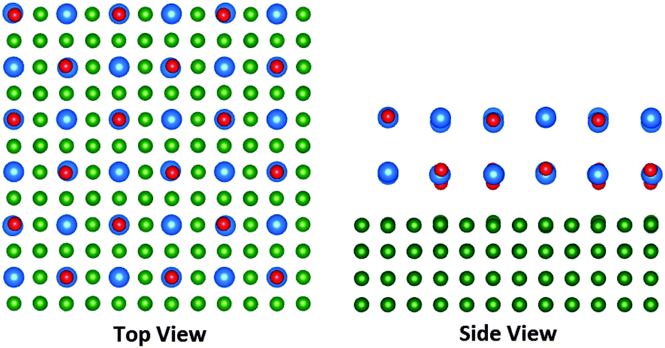 | ||
| Fig. 1 The unit cell of CsBr(2 ML)/Cu(100). The Cs ions are depicted in blue, Br ions in red, and Cu ions in green. | ||
The interatomic Cs–Br distance of bulk β-CsBr has been calculated as 3.65 Å, close to the experimentally measured separation of 3.62 Å.25 The calculated lattice parameter of bulk Cu is 3.61 Å, in agreement with the experimental value of 3.61 Å.27 The work function has been calculated by taking the average of the electrostatic potential across the x–y plane for each value of z, such that an averaged 1D potential in the z-direction is constructed. The change in the work function has then been calculated as the difference between the potential on either side of the surface (i.e. at the interface between the vacuum, and the interface between clusters of CsBr).
The band gap of CsBr calculated using the PBE functional is 5.0 eV, which is significantly less than the experimental band gap (7.30 eV) as established by UV photoelectron spectroscopy (UPS).28 However, PBE describes well the electronic structure of Cu. We use a large Cu surface area, which is necessary in order to validate the Γ-point approximation as well as to provide enough surface area such that a number of different CsBr clusters may be placed on the surface. Therefore calculations with hybrid functionals, such as PBE0, are prohibitively expensive. We note that previous studies of the MgO/Ag interface found little difference in calculated interfacial separation and Ag work function shift under either the GGA description (PBE) and hybrid functional description (HSE06 and PBE0).16,17 Moreover, the use of a hybrid functional also leads to a distorted metal band structure and consequently a qualitatively incorrect description of the screening properties of the metal.29
Long-range van der Waals forces have been shown to play a significant role in determining the metal–oxide distance and hence the work function reduction at metal/oxide interfaces16 and are not accounted for under the PBE description. We have included the van der Waals interaction between CsBr and Cu(100) in some calculations using Grimme's D2 method (PBE + D2).30 Although there have been major developments of DFT functionals, which attempt to account for dispersion forces,31–33 these remain largely untested in metal/insulator systems. Recent studies have also suggested the improved results of PBE + D2 over PBE + D3 in alkali halides for properties such as cohesion energy,34,35 and, due to their relative conceptual simplicity, they have been included here. The same study has provided D2 parameters for Cs+ ions, which have been used here. Other parameters have been taken from Grimme's original paper.30 Although the D2 method has been used to describe metal–insulator dispersion forces in other studies,16,17 the D2 parameters have been derived from non-metallic systems, and as such their capacity to accurately describe Cs–Cu and Br–Cu forces is uncertain.
3 Results
3.1 Cu work function shift at full CsBr coverage
The work function values for the 288- and 392-atom Cu(100) surfaces have been calculated as 4.47 and 4.53 eV, respectively, in good agreement with the experimental value of 4.59 eV.12 The Cs atom adsorption energy was calculated as 1.78 eV on both surfaces. A density of states (DOS) plot of the 392-atom Cu(100) surface is depicted in Fig. 2.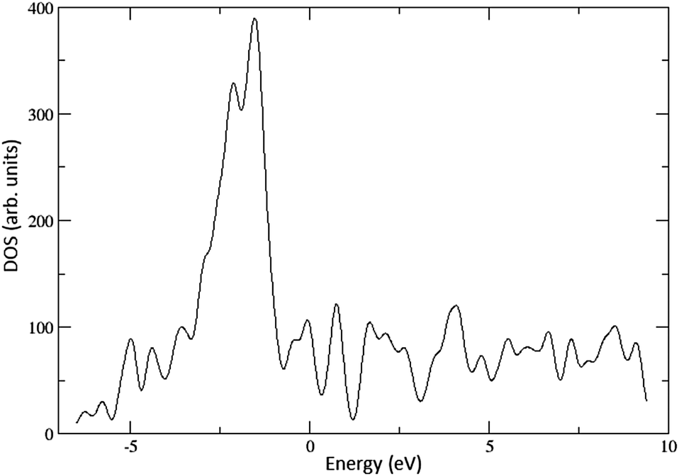 | ||
| Fig. 2 The calculated density of states for the Cu(100) surface. | ||
The calculated DOS reproduces the most pertinent features of the DOS constructed from XPS.36 The plot is characterised by two peaks – a small shoulder near the Fermi level energy, and a significantly larger peak at lower energies, reaching a maximum between 1 and 1.5 eV below the Fermi level. A reduction of the work function, or in other words a shift upwards of these states by 1–1.5 eV would result in a significantly increased cross-section of interaction with photons incident on the surface. This is one possible explanation for the observed increase in quantum efficiency after the application of CsBr films.7,9
The 288-atom Cu periodic cell has been used to calculate the perfect interface with CsBr films at full coverage. CsBr films of 2, 3, 4 and 5 monolayers (MLs) have been placed on top of the Cu surface and allowed to relax. The interfacial separation, defined as the difference between the average of the z-coordinates of the top layer of Cu atoms, and the z-coordinates of the interface layer Cs and Br atoms, has been estimated as 3.45 Å for films of 2 ML coverage, decreasing slightly as the films thicken. The Cu work function shift is 1.4 eV and 1.5 eV for the 2 and 4 layer films, respectively.
The sensitivity of work function shift to calculated interfacial separation is well attested in the literature.15,16,37 In order to gauge the dependence of estimated work function shift on the interfacial separation, we performed a series of single-point energy calculations varying the distance from the Cu surface from a minimum of 2.5 Å to a maximum of 4 Å. The observed relationship is linear to a good approximation. The range of experimental estimates of a work function shift between 1–2 eV corresponds to the interfacial separation in the range of 3–4 Å.
3.2 van der Waals forces and the interfacial separation
The interface geometry and work function shift has then been recalculated with the inclusion of van der Waals forces using the D2 approximation.30 The resulting work function shift and the interfacial separation for 2, 3 and 4 MLs of CsBr has been calculated. The interfacial separation decreases to 3.0 Å for all films. The work function reduction consequently increases by 1.75 eV in the 2 ML case to 1.9 eV in the 4 ML case.The inclusion of the van der Waals interaction decreases the interface separation by about 0.45 Å. Although there is some reduction in the CsBr interface rumpling, the work function shift is consistent with the PBE value at a similar interfacial separation of 3.0 Å. We note that previous studies suggest that D2 has a tendency to over-bind between metal and insulator,38,39 possibly due to the fact that D2 parameters are derived from insulator–insulator interactions. Since the inclusion of the van der Waals interaction in our system is equivalent to decreasing the interfacial separation, it does not significantly add to our physical understanding of the mechanisms of LA. Therefore further calculations were performed at the PBE level.
3.3 Cu work function shift at rough Cu/CsBr interface
As the experimental measurements of the CsBr/Cu work function shift vary by around 1 eV, it is possible that the different values reflect a difference in film quality, and variations in local structure at the interface. In order to model the effects of the Cu surface coverage by CsBr films, clusters of 2, 3 and 4 MLs corresponding to coverages of 21%, 36% and 75% have been placed on top of the larger 392-atom Cu periodic cell, and allowed to fully relax. The resulting work function shifts are shown in Table 1.| Coverage (%) | MLs | ϕ | Δϕ | |
|---|---|---|---|---|
| CsBr/Cu(100) | 21 | 2 | 3.44 | 1.09 |
| 3 | 3.29 | 1.24 | ||
| 4 | 3.23 | 1.30 | ||
| 36 | 2 | 3.11 | 1.42 | |
| 3 | 3.03 | 1.50 | ||
| 4 | 2.95 | 1.58 | ||
| 75 | 2 | 3.03 | 1.50 | |
| 3 | 2.95 | 1.58 | ||
| 4 | 2.93 | 1.60 | ||
The Br anions tend to relax towards and Cs cations away from the cluster. The shift in work function rises from 1.3 to 1.6 eV for 4 ML CsBr films as the coverage increases from 21% to 75%. Curiously, the largest work function shift, as a result of deposition of clusters of 75% coverage (1.6 eV), is slightly larger than the calculated shift on the smaller surface for films of full coverage (1.5 eV). This is partially explicable due to the dipoles which exist at the corners of CsBr clusters. The clusters also have a slightly smaller interfacial separation than the perfect films, of the order of 0.1 Å, which further increases the work function shift.
3.4 Mechanisms of laser activation of CsBr/Cu interface
The “laser activation” of a photocathode refers to the increase in quantum efficiency following a period of UV laser irradiation. It has been suggested that this is due to defect creation at and around the interface. In particular, F-centres have been suggested as candidates for so-called intra-band-gap absorption states (IBASs), which have been posited as being responsible for the increase in quantum efficiency in CsBr/Cr photocathodes by functioning as electron injectors.1,40The irradiation of CsBr films with single 4.66 eV photons cannot excite inter-band transitions and create excitons, which are known to be responsible for photo-desorption of CsBr films and creation of Br vacancies, F-centres, in the bulk and at the surface of CsBr.26 This requires two-photon excitation, hence the long laser activation period. The recent calculations24 suggest that the electronic excitation of surface F-centres by electrons emitted from Cu (Franck–Hertz effect) can lead to emission of Cs atoms adjacent to surface F-centres, creating neutral anion–cation vacancy dimers (di-vacancies) at the CsBr surface. Below we consider the effect of F-centres and di-vacancies on the work function shift of Cu(100).
| Layer | E F (eV) | Δϕ (eV) | |
|---|---|---|---|
| CsBr(4 ML)/Cu(100) | 1 | 3.58 | 1.57 |
| 2 | 3.98 | 1.66 | |
| 3 | 3.95 | 1.65 | |
| 4 | 4.34 | 2.04 | |
| β-CsBr | — | 5.74 | — |
The F-centre formation energies in the thin films are smaller than the formation energy of an F-centre in the bulk of β-CsBr, by approximately 2 eV. The formation energies decrease as the proximity of the vacancy site to the interface increases, with the most favourable site at the interface. The geometry around the fully-relaxed F-centre at the interface is depicted in Fig. 3.
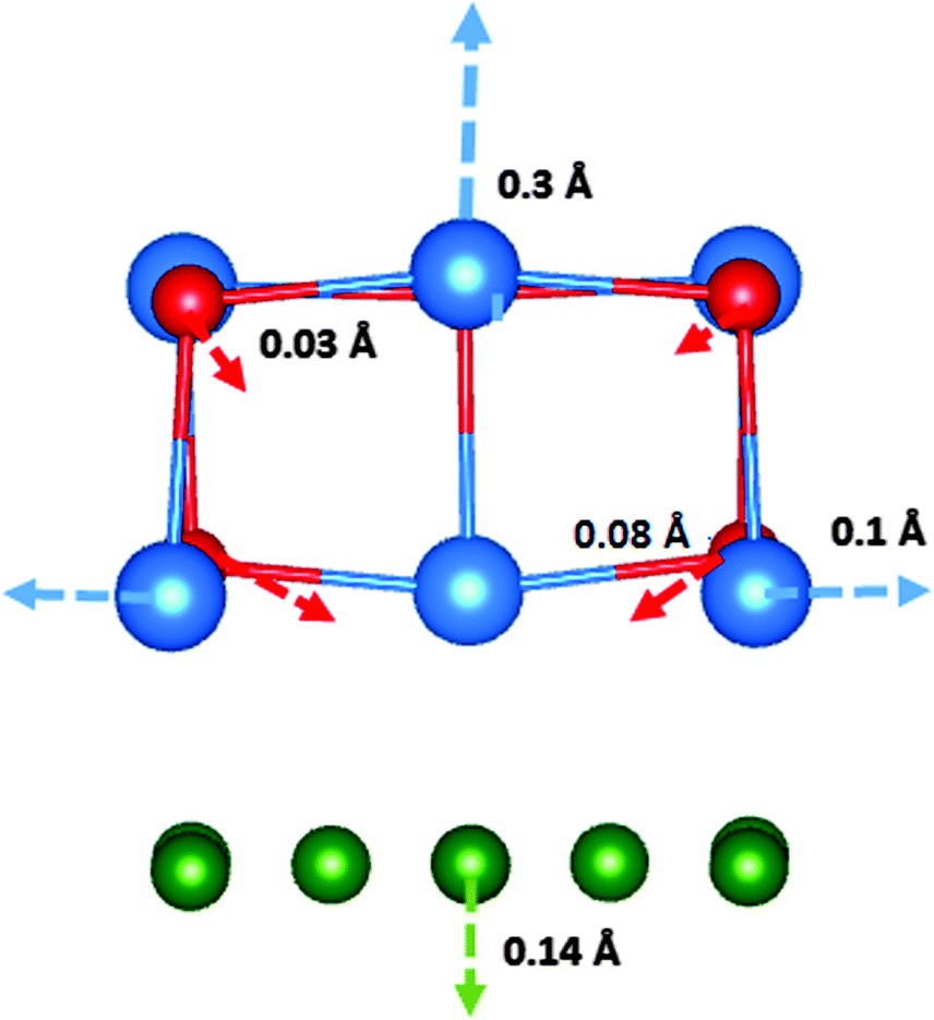 | ||
| Fig. 3 The local geometry of an anion vacancy at the interface, with nearest neighbour displacements. The length of the arrow is approximately proportional to the magnitude of displacement. The Cs ions are depicted in blue, Br ions in red, and Cu ions in green. | ||
Analysis of the electron density distribution reveals, however, that the electron at the vacancy site is donated to the Cu(100) surface, such that the defect is formally positively-charged and resembles an F+-centre. The position of the F-centre energy level in the bulk CsBr has been determined to be 2.0 eV below the conduction band by optical absorption spectroscopy.41,42 This is much higher than the Cu(100) Fermi level position with respect to vacuum (see Table 1), hence the electron transfer into Cu. The local anions relax towards the vacancy, and cations away from it. A spin density plot of the system shows the extra electron to be delocalised over the Cu(100) surface. This is also true of the F-centre in all layers of the CsBr films.
A recent publication has estimated the barrier to F+-centre migration as 0.3 eV in the bulk of α-CsBr.42 If we assume a similar barrier here, we would expect vacancies created in the bulk near the interface to diffuse preferentially to the interface. As an F+-centre is positively charged, it should polarize the metal, giving rise to an attractive force. The work function reduces further as a result of the defect, by 0.07 eV with respect to the defect-less system.
To investigate the effect of concentration of F+-centres at the interface on the work function shift, we have also modelled two F+-centres in various configurations at the CsBr/Cu(4 ML) interface. Fig. 4 indicates the positions where pairs of F-centres have been modelled, with Table 3 giving the corresponding formation energies and work function shifts.
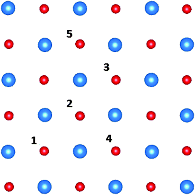 | ||
| Fig. 4 All unique combinations of two F-centres in the interface layer of the unit cell. F-centres have been modelled at site 1 and 2, 3, 4 and 5. The Cs ions are depicted in blue, Br ions in red. | ||
| Position | E F (eV) | Δϕ (eV) | |
|---|---|---|---|
| CsBr(4 ML)/Cu(100) | 2 | 7.15 | 1.61 |
| 3 | 7.12 | 1.62 | |
| 4 | 7.14 | 1.62 | |
| 5 | 7.08 | 1.62 |
As the positively-charged F+-centres experience mutual Coulomb repulsion, vacancy sites more distant from each other are more energetically favourable, (i.e. F+-centres at positions 1 and 5 are of lower energy than at positions 1 and 2). This is mitigated to some extent by the shared relaxation of neighbouring ions, such that all configurations have energies within a range of 0.07 eV. The calculations are restricted by the size of the unit cell, but the work function changes by approximately 0.05 eV with respect to the single isolated F+-centre in all cases. Based on these calculations we estimate that a high density of anion vacancies may lead to a reduction of the work function by approximately 0.1 eV with respect to the clean CsBr/Cu interface.
We note that an electrostatic correction for the defect interaction with images in the neighbouring supercells in the periodic dimensions has not been applied to the charged defects here. The periodic cell is neutral overall and this correction, if any, is expected to be small. However, accurately calculating such corrections for 2D systems of the type considered here is still challenging. The Parry method43,44 enables a point charge correction to be calculated for slabs, but does not allow for a varying dielectric profile. A new method developed in ref. 45 allows the dielectric profile to vary in one dimension only. Both these methods assume charge compensation by a homogeneous background, which would be incorrect for our model. The details of the compensating charge are found to be crucial for accurate corrections. In our model, this is an image charge in the metal substrate, which has accepted the removed electron. In any case, as our simulation cell is neutral, the interaction should be significantly weaker than in a formally charged cell.46
Di-vacancies can diffuse through the lattice by 90° rotations. Rotations proceed by neighbouring Br and Cs ions moving into the vacancy site, leaving behind a new vacancy. The diffusion barrier in bulk β-CsBr has been estimated by performing climbing-image nudged elastic band47,48 (CI-NEB) calculations with five replicas. The barrier to rotation via Cs and Br ionic motion has been calculated as 0.65 and 0.55 eV, respectively. At these energies we can expect di-vacancies to move through the lattice, but at a slower rate than H-centre or F+-centre diffusion, which have barriers of approximately 0.05 and 0.3 eV, respectively.42
In order to examine the behaviour of di-vacancies around the interface, and their effect on the work function, di-vacancies have been placed in three different configurations at the interface; parallel to the interface, and perpendicular to the interface with both the Br and Cs vacancy in the interface layer. The di-vacancy parallel to the interface is of the lowest energy. The perpendicular configuration with the Br vacancy in the interface layer is higher in energy by 0.1 eV, and that with the Cs vacancy in the interface layer is higher again by 0.6 eV.
The work function shift as a result of the di-vacancy in the interface layer (i.e. parallel to the interface) is calculated as 0.16 eV. The geometry of the di-vacancy is depicted in Fig. 5. Two Br anions neighbouring the cation vacancy relax towards Cu to a particularly large extent (0.9 Å) as a result of the defect. The reduction in Mullikan charge of the Br ions (Δq = 0.6 |e|) suggests that the large displacement is due to bond formation between the Br− ions and Cu+ ions of the surface. The charge transfer of two electrons from Br ions neighbouring the di-vacancy is one possible explanation for the reduction in work function as a result of the defect.
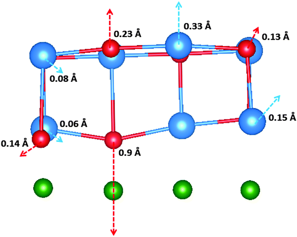 | ||
| Fig. 5 The local geometry of a di-vacancy at the interface, with the nearest neighbour displacements. The length of the arrows are approximately proportional to the magnitudes of displacement. The Cs ions are depicted in blue, Br ions in red, and Cu ions in green. | ||
We have also modelled the effect of two adjacent di-vacancies in a square formation in the interface layer. The resulting shift of the Cu(100) work function is calculated as 0.28 eV. The di-vacancy and tetra-vacancy correspond to ionic depletion at the interface of 5.5% and 11%, respectively. These results suggest that di-vacancy aggregation at the interface results in a reduction of the work function by an amount close to the shift seen in experiment during the activation period. F-centres by contrast induce a work function reduction approximately half as large.
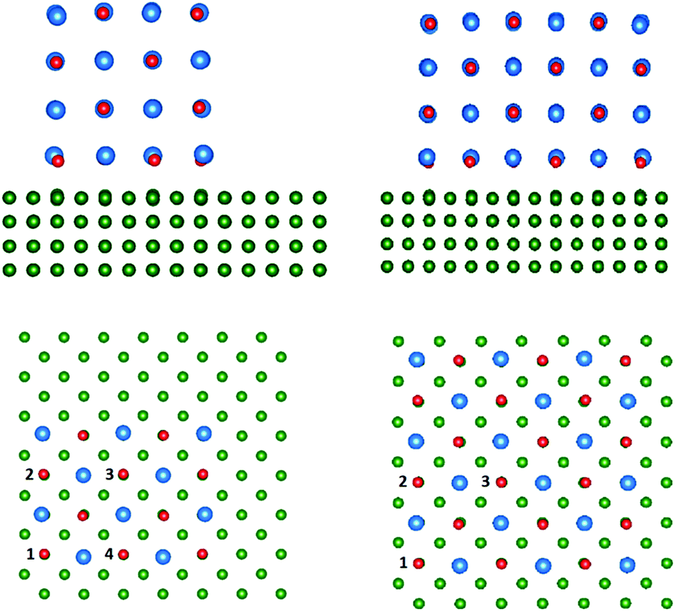 | ||
| Fig. 6 The geometry of relaxed 4 ML CsBr clusters of 21% and 75% coverage on the Cu(100) surface. The Cs ions are depicted in blue, Br ions in red, and Cu ions in green. | ||
| Coverage (%) | Site | E F | Δϕ | |
|---|---|---|---|---|
| CsBr/Cu(100) | 21 | None | — | 1.30 |
| 1 | 3.38 | 1.44 | ||
| 2 | 3.45 | 1.44 | ||
| 3 | 3.52 | 1.41 | ||
| 4 | 3.61 | 1.44 | ||
| 75 | None | — | 1.60 | |
| 1 | 3.38 | 1.72 | ||
| 2 | 3.49 | 1.70 | ||
| 3 | 3.60 | 1.68 | ||
In all cases an electron from an F-centre is transferred to Cu(100) forming a positively charged vacancy, F+-centre. The most energetically favourable sites for F+-centre formation are corner sites, followed by side sites, with the sites in the centre of the clusters being least energetically favourable. The increase in shift of the work function as a consequence of F-centre formation is slightly larger in the smaller cluster than the larger one. Both clusters suggest that an F+-centre can shift the work function by approximately 0.1–0.15 eV.
4 Discussion and conclusions
We have investigated the effect of perfect and rough CsBr thin films on the Cu(100) surface on the Cu work function as a function of coverage and film thickness using DFT. The effects of F-centres and di-vacancies at various positions at the interface were studied to propose possible explanations for the observed increase in the quantum efficiency of Cu photocathodes after coating with CsBr films and further laser activation. The inclusion of van der Waals forces leads to a further reduction in the interfacial separation and work function of the films.Our calculations predict a work function shift in the range 1.5–1.7 eV further shifting by about 0.1–0.15 eV following the creation of F-centres at the interface as a by-product of laser irradiation. Modelling partial coverage of the Cu surface predicts similar work function shifts for coverages over 50%.
Indeed clusters of coverage around 75% actually induce a larger work function shift than films of full coverage. This is not inconsistent with existing models of insulating films deposited on metals. The clusters all have a smaller interfacial separation with the Cu substrate than the films of full coverage, and contain corners sites where the presence of dipoles further act to decrease the work function. Experimentally, it has been observed that films of partial Cs coverage induce a work function shift larger than films of 1 ML thickness and above49–51 and that maximum photoemission occurs for Cs deposited on Au(111) at a coverage of between 0.2–0.25 ML.52 This suggests that the deposition of Cs atoms may decrease the work function to a larger extent than bulk-like clusters or complete films, and that the charge transfer from Cs to metal induces a larger shift than that due to compression of the metal wavefunctions due to an insulator at the interface.
The CsBr films used experimentally are 3–7 nm thick.7,9 As the 266 nm photon energies are below the surface and bulk exciton threshold, excitons can be excited due to two-photon processes preferably in the bulk of the film. These excitons can separate into F–H pairs, such that, following previous studies, the H-centres which reach the surface form weakly adsorbed Br atoms. The latter can desorb from the surface with thermal energies.26 F-centres in the bulk have diffusion barriers of the order of 1 eV.42,53 However, near the interface, donation of the electron to metal results in the formation of the comparatively mobile F+-centre, which experiences an attractive force towards the metal due to induced image charge. F+-centres show a preference to diffuse to the interface, although their positive charge discourages their segregation at the interface. Our calculations are either at or above equilibrium saturation density, and the predicted maximum reduction of the work function is about 0.15 eV. This is smaller than the shift normally associated with laser activation of CsBr/Cu photocathodes of around 0.3 eV.
Di-vacancies are formed at the CsBr/Cu surface as a result of laser irradiation.24 Their diffusion across the surface is inhibited by electrons photo-emitted from the metal, which can trap at the defect site. The thermal barrier to electron escape is, however, small (∼0.3 eV24), such that the di-vacancies charge and discharge in a dynamic process of electron emission and replenishment during irradiation. While in the neutral charge state, some di-vacancies may rotate and diffuse towards the CsBr/Cu interface. CI-NEB calculations of the diffusion barrier to di-vacancy motion suggest they should be mobile at room temperature, and the image charge in the metal induced by the dipole facilitates their diffusion towards the interface. Calculations of di-vacancies and a pair of adjacent di-vacancies at the interface demonstrate work function reductions of 0.16 and 0.28 eV, respectively. These calculations suggest that the laser activation can be explained by the photo-induced creation of Br vacancies and Cs–Br di-vacancies and their segregation at the interface.
To summarise, our calculations explain how the observed increase of the quantum efficiency of CsBr/Cu photocathodes can be caused by the shift of Cu(100) workfunction due to CsBr film on the surface. We suggest the mechanism by which operation of the photocathode using 266 nm photons leads to the CsBr film degradation due to creation of Cs and Br vacancies and further reduction of the Cu(100) work function.
Acknowledgements
MTEH is grateful to EPSRC for financial support. WPH acknowledge support from the US Department of Energy (DOE), Office of Science, Office of Basic Energy Sciences, Division of Chemical Sciences, Geosciences and Biosciences. Pacific Northwest National Laboratory is a multiprogram national laboratory operated for DOE by Battelle. Our access to the Archer facility is provided via our membership of the UK's HPC Materials Chemistry Consortium, which is funded by EPSRC grant EP/F067496. We are grateful to T. Durrant for useful discussions and help in calculations.References
- J. R. Maldonado, Z. Liu, Y. Sun, P. Pianetta and F. W. Pease, J. Vac. Sci. Technol., B: Microelectron. Nanometer Struct. – Process., Meas., Phenom., 2006, 24, 2886–2891 CrossRef CAS.
- J. Maldonado, Y. Sun, Y. Liu, X. Liu, S. Tanimoto, P. Pianetta and F. Pease, J. Vac. Sci. Technol., B: Microelectron. Nanometer Struct. – Process., Meas., Phenom., 2008, 26, 2085–2090 CAS.
- J. R. Maldonado, S. T. Coyle, B. Shamoun, M. Yu, M. Gesley and P. Pianetta, J. Vac. Sci. Technol., B: Microelectron. Nanometer Struct. – Process., Meas., Phenom., 2004, 22, 3025–3031 CrossRef CAS.
- J. R. Maldonado, Z. Liu, Y. Sun, S. Schuetter, P. Pianetta and R. F. W. Pease, J. Vac. Sci. Technol., B: Microelectron. Nanometer Struct. – Process., Meas., Phenom., 2007, 25, 2266–2270 CrossRef CAS.
- J. R. Maldonado, P. Pianetta, D. H. Dowell, J. Smedley and P. Kneisel, J. Appl. Phys., 2010, 107, 013106 CrossRef.
- J. R. Maldonado, Z. Liu, D. H. Dowell, R. E. Kirby, Y. Sun, P. Pianetta and F. Pease, Microelectron. Eng., 2009, 86, 529–531 CrossRef CAS.
- W. He, S. Vilayurganapathy, A. G. Joly, T. C. Droubay, S. A. Chambers, J. R. Maldonado and W. P. Hess, Appl. Phys. Lett., 2013, 102, 071604 CrossRef.
- J. R. Maldonado, P. Pianetta, D. H. Dowell, J. Corbett, S. Park, J. Schmerge, A. Trautwein and W. Clay, Appl. Phys. Lett., 2012, 101, 231103 CrossRef.
- L. Kong, A. G. Joly, T. C. Droubay, Y. Gong and W. P. Hess, Appl. Phys. Lett., 2014, 104, 171106 CrossRef.
- T. Vecchione, J. R. Maldonado, S. Gierman, J. Corbett, N. Hartmann, P. A. Pianetta, L. Hesselink and J. F. Schmerge, Phys. Rev. ST Accel. Beams, 2015, 18, 040701 CrossRef.
- J. Maldonado, Z. Liu, R. Kirby, Y. Sun, P. Pianetta and F. Pease, Phys. Rev. Spec. Top. – Accel. Beams, 2008, 11, 060702 CrossRef.
- P. O. Gartland, S. Berge and B. J. Slagsvold, Phys. Rev. Lett., 1972, 28, 738–739 CrossRef CAS.
- D. H. Dowell, I. Bazarov, B. Dunham, K. Harkay, C. Hernandez-Garcia, R. Legg, H. Padmore, T. Rao, J. Smedley and W. Wan, Radiat. Prot. Dosim., 2010, 119, 398–401 Search PubMed.
- L. Kong, A. G. Joly, T. C. Droubay and W. P. Hess, Chem. Phys. Lett., 2015, 621, 155–159 CrossRef CAS.
- S. Prada, U. Martinez and G. Pacchioni, Phys. Rev. B: Condens. Matter Mater. Phys., 2008, 78, 235423 CrossRef.
- S. Ling, M. B. Watkins and A. L. Shluger, Phys. Chem. Chem. Phys., 2013, 15, 19615–19624 RSC.
- S. Ling, M. B. Watkins and A. L. Shluger, J. Phys. Chem. C, 2013, 117, 5075–5083 CAS.
- J. P. Perdew, K. Burke and M. Ernzerhof, Phys. Rev. Lett., 1996, 77, 3865–3868 CrossRef CAS PubMed.
- J. Hutter, M. Iannuzzi, F. Schiffmann and J. VandeVondele, Wiley Interdiscip. Rev.: Comput. Mol. Sci., 2014, 4, 15–25 CrossRef CAS.
- S. Goedecker, M. Teter and J. Hutter, Phys. Rev. B: Condens. Matter Mater. Phys., 1996, 54, 1703–1710 CrossRef CAS.
- C. Hartwigsen, S. Goedecker and J. Hutter, Phys. Rev. B: Condens. Matter Mater. Phys., 1998, 58, 3641–3663 CrossRef CAS.
- M. Krack, Theor. Chem. Acc., 2005, 114, 145–152 CrossRef CAS.
- J. VandeVondele and J. Hutter, J. Chem. Phys., 2007, 127, 114105 CrossRef PubMed.
- M. T. E. Halliday, A. G. Joly, W. P. Hess and A. L. Shluger, J. Phys. Chem. C, 2015, 119, 24036–24045 CAS.
- M. Kiguchi, S. Entani, K. Saiki and A. Koma, Surf. Sci., 2003, 523, 73–79 CrossRef CAS.
- M. T. E. Halliday, A. G. Joly, W. P. Hess, P. V. Sushko and A. L. Shluger, J. Phys. Chem. C, 2013, 117, 13502–13509 CAS.
- M. E. Straumanis and L. S. Yu, Acta Crystallogr., Sect. A: Found. Crystallogr., 1969, 25, 676–682 CrossRef CAS.
- K. Teegarden and G. Baldini, Phys. Rev., 1967, 155, 896–907 CrossRef CAS.
- J. Paier, M. Marsman, G. Kresse, I. C. Gerber and J. G. Angyan, J. Chem. Phys., 2006, 124, 154709 CrossRef CAS PubMed.
- S. Grimme, J. Comput. Chem., 2006, 27, 1787–1799 CrossRef CAS PubMed.
- J. F. Dobson and T. Gould, J. Phys.: Condens. Matter, 2012, 24, 073201 CrossRef PubMed.
- T. Bjorkman, A. Gulans, A. V. Krasheninnikov and R. M. Nieminen, J. Phys.: Condens. Matter, 2012, 24, 424218 CrossRef CAS PubMed.
- J. Klimes and A. Michaelides, J. Chem. Phys., 2012, 137, 120901 CrossRef PubMed.
- S. Grimme, S. Ehrlich and L. Goerigk, J. Comput. Chem., 2011, 32, 1456–1465 CrossRef CAS PubMed.
- F. Zhang, J. D. Gale, B. P. Uberagua, C. R. Stanek and N. A. Marks, Phys. Rev. B: Condens. Matter Mater. Phys., 2013, 88, 054112 CrossRef.
- S. Huefner, G. K. Wertheim, N. V. Smith and M. M. Traum, Solid State Commun., 1972, 11, 323–326 CrossRef CAS.
- L. Giordano, F. Cinquini and G. Pacchioni, Phys. Rev. B: Condens. Matter Mater. Phys., 2006, 73, 045414 CrossRef.
- S. Ehrlich, J. Moellmann, W. Reckien, T. Bredow and S. Grimme, ChemPhysChem, 2011, 12, 3414–3420 CrossRef CAS PubMed.
- P. L. Silvestrelli and A. Ambrosetti, Phys. Rev. B: Condens. Matter Mater. Phys., 2015, 91, 195405 CrossRef.
- Z. Liu, J. Maldonado, Y. Sun, P. Pianetta and R. F. W. Pease, Appl. Phys. Lett., 2006, 89, 111114 CrossRef.
- H. Rabin and J. Schulman, Phys. Rev., 1962, 125, 1584–1596 CrossRef CAS.
- M. T. E. Halliday, W. P. Hess and A. L. Shluger, J. Phys.: Condens. Matter, 2015, 27, 245501 CrossRef CAS PubMed.
- D. Parry, Surf. Sci., 1975, 49, 433–440 CrossRef CAS.
- J. R. Rustad, E. Wasserman and A. R. Felmy, Surf. Sci., 1999, 424, 28–35 CrossRef CAS.
- H.-P. Komsa and A. Pasquarello, Phys. Rev. Lett., 2013, 110, 095505 CrossRef PubMed.
- G. Makov and M. C. Payne, Phys. Rev. B: Condens. Matter Mater. Phys., 1995, 51, 4014–4022 CrossRef CAS.
- G. Henkelman, B. P. Uberuaga and H. Jónsson, J. Chem. Phys., 2000, 113, 9901–9904 CrossRef CAS.
- G. Henkelman and H. Jónsson, J. Chem. Phys., 2000, 113, 9978–9985 CrossRef CAS.
- S. Yun, Z. Liu and P. Pianetta, J. Vac. Sci. Technol., A, 2007, 25, 1351–1356 Search PubMed.
- J. Lee, C. Lin and A. A. Demkov, Phys. Rev. B: Condens. Matter Mater. Phys., 2013, 87, 165103 CrossRef.
- V. Ageev, Y. Kuznetsov and N. Potekhina, Phys. of the Sol. Stat., 2005, 47, 1784–1790 CrossRef CAS.
- J. L. LaRue, J. D. White, N. H. Nahler, Z. Liu, P. A. Pianetta, D. J. Auerbach and A. M. Wodtke, J. Chem. Phys., 2008, 129, 024709 CrossRef CAS PubMed.
- A. M. Stoneham, Theory of Defects in Solids – Electronic structure of defects in insulators and semiconductors, Oxford University Press, 1975 Search PubMed.
| This journal is © the Owner Societies 2016 |