
Resistive switching properties of epitaxial BaTiO3−δ thin films tuned by after-growth oxygen cooling pressure†
Yooun
Heo
a,
Daisuke
Kan
b,
Yuichi
Shimakawa
bc and
Jan
Seidel
*a
aSchool of Materials Science and Engineering, University of New South Wales, Sydney, NSW 2052, Australia. E-mail: jan.seidel@unsw.edu.au
bInstitute for Chemical Research, Kyoto University, Gokasho, Uji, Kyoto 611-0011, Japan
cJapan Science and Technology Agency, CREST, Uji, Kyoto 611-0011, Japan
First published on 25th November 2015
Abstract
BaTiO3−δ, i.e. oxygen-deficient barium titanate (BaTiO3), thin films grown on GdScO3(110) substrates with SrRuO3 conductive electrodes by pulsed laser deposition are studied by X-ray diffraction and conductive AFM to characterize their structure and nanoscale electronic properties. Bias- and time-dependent resistive switching measurements reveal a strong dependence on the oxygen vacancy concentration, which can be tuned by after-growth oxygen cooling conditions of thin films. The results indicate that the resistive switching properties of BaTiO3−δ can be enhanced by controlling oxygen deficiency and provide new insight for potential non-volatile resistive random-access memory (RRAM) applications.
1 Introduction
Barium titanate (BaTiO3) is well known as a promising ferroelectric material with a high dielectric constant and superior chemical stability that is widely used in actuator and sensor devices.1–3 Considerable research efforts have been made to investigate the suitability of BaTiO3 for storage applications based on e.g. tunnel junction concepts4–8 and resistive switching, which is usually observed in capacitor-like structures consisting of various metal oxides including multi-elemental perovskite-type oxides9–12 and binary oxides.13–17 The observed resistive switching mechanisms and behaviours are diverse and some possible scenarios have been proposed. Two broad types can be considered to classify these mechanisms in terms of microscopic physics. One is based on the ionic movement18 or the formation of conductive filaments and channels, e.g. through local redox reactions. Another interface driven mechanism is based on the electromigration of oxygen vacancies,19 which induces a change in the valence states of cations in the metal oxide, resulting in a change in the electronic states and thus alteration of conductivity. Despite intensive studies on RRAM concepts, the exact switching mechanism based on physical analysis for various materials is not fully investigated yet. Since the very first report of a resistive switching effect in ferroelectric niobium oxide,20 much attention has been given to ferroelectric perovskite titanates21–24 in the study of ferroelectric resistive switching. In addition to these studies of driving mechanisms, the aspect of engineering thin films and structures was also investigated in ferroelectric perovskite titanates, e.g. Cr-doped (Ba,Sr)TiO3,10 and BaTiO3 films with an electrode of La0.7Ca0.3MnO3.25 More recently, the temperature dependence of I–V characteristics in BaTiO3/La0.8Ca0.2MnO3 was reported, showing diode-like asymmetric characteristics below 250 K and resistive switching behaviour at higher temperatures.26 As such, there has been a vast amount of efforts to exploit the potential of materials in various aspects of their functional properties. Among the various models proposed for resistance switching, the oxygen migration based model has attracted much attention due to the notable demonstration of switching behaviours at the Pt/TiO2 interface.27–32 In many oxide systems, oxygen vacancies behave as mobile donors33–35 and electrical control of their concentration at the metal/oxide interface is attractive for memory applications if tuning and strict control of oxygen content is possible.In this paper, we report on the well-defined resistive switching properties of oxygen deficient epitaxial BaTiO3−δ films fabricated under defined after-growth oxygen cooling conditions by using nanosized electric characterization via conductive AFM (c-AFM) at room temperature. Unlike previous studies on switchable diodes, we used several oxygen deficient films of barium titanate as a switching element, since their electrical conductivity can be controlled simply by an additional post-cooling process, i.e. annealing in a defined oxygen environment, resulting in a modulation of the oxygen vacancy concentration. Current–voltage behaviour from I–V curve measurements shows that the current magnitude is strongly dependent on the oxygen vacancy content in the films, providing a clue to the mechanism involved. Bias- and time-dependent I–V curve measurements show that resistance switching properties can be tuned by varying the amplitude and time duration of the applied bias as a means to control the device properties of the system. BaTiO3−δ films with large amounts of oxygen vacancies exhibit clear rectifying I–V characteristics and hysteretic behaviour. The large discrepancy observed between the onset voltage of electrical current starting to flow and the coercive voltage required for ferroelectric switching suggests that the ferroelectric contribution to resistive switching is rather small for samples containing a considerable amount of oxygen vacancies. Instead, our results reveal that the local distribution of oxygen vacancies and their bias dependent movement play a crucial role in the emergence of the resistive switching effect. Furthermore, resistive switching characteristics in the pulse-voltage mode are presented to evaluate the repeatability and potential for device applications.
2. Experimental methods
2.1 Sample preparation
60 nm thick oxygen deficient barium titanate BaTiO3−δ (BTO) films were epitaxially grown by pulsed laser deposition on GdScO3(110)o (GSO) substrates capped by a 10–15 nm-thick SrRuO3 (SRO) layer that served as a bottom electrode36 at 700 °C (the subscript o notation denotes the orthorhombic perovskite). GSO (ao = 5.49 Å, bo = 5.75 Å, co = 7.93 Å) has a closely matched in-plane lattice parameter to BTO (a = b = 3.99 Å, c = 4.04 Å) with bulk lattice mismatch strain of 0.67%. The BTO layer was deposited from a sintered ceramic stoichiometric BTO target using a KrF excimer laser (λ = 248 nm) at 1.5 J cm−2 and 2 Hz repetition rate. For the deposition of the SRO layer, the Ru-rich SrRu1.1O3 target was used to minimize the possible Ru deficiencies and was pulsed at 1.0 J cm−2. The oxygen pressure during the deposition of BTO and SRO was set to 25 and 100 mTorr, respectively. To vary the amount of oxygen vacancies in the BTO layer, the deposited films were cooled under various oxygen pressures ranging from 50 μTorr to 100 Torr.37,38 Controlling the amount of oxygen vacancies and their distribution can be used to tune the conductivity in perovskite oxides.39–412.2 Characterization of structural and physical properties
The crystal structure and thin film orientation were analyzed using a conventional four-circle diffractometer (PANalytical X’PertMRD) at Kyoto University. A commercial scanning probe microscope system (AIST-NT SmartSPM) was used to perform the measurements of c-AFM and PFM at UNSW. A conductive diamond coated tip with a force constant of around 40–50 N m−1 (DCP20, NT-MDT) was used for imaging and I–V curves. For pulsed mode measurements, the voltage pulses and current reading for resistive switching were monitored using a built-in oscilloscope in SmartSPM.3. Results and discussion
Atomic force microscopy (AFM) images show that our PLD-grown samples have smooth surface morphology with the root-mean-square (rms) surface roughness around 0.25 nm as shown in the ESI† (Fig. S1). No obvious protruding surface features were observed in the samples, indicating a two dimensional growth of the BTO layer.24Fig. 1a shows 2θ–θ profiles around the (220)o GSO Bragg reflection for the films grown at various oxygen cooling pressures ranging from 50 μTorr to 100 Torr. The films show only the (002) BTO reflection and (220)o SRO reflections without any reflections from impurity phases, confirming the epitaxial growth of the films on the GSO substrate. We also performed X-ray reciprocal space maps (RSMs). Fig. 1b displays the semi-logarithmic contour plot of the RSM around the (444)o GSO Bragg reflection for the films prepared by cooling under an oxygen pressure of 25 mTorr. The (103) BTO, (444)o SRO and (444)o GSO reflections are seen at the same position along the horizontal axis, indicating that the in-plane lattices of BTO and SRO are fixed by the substrate. Essentially the same results are seen for all fabricated films. The (103) BTO reflection position along the vertical axis, which corresponds to the out-of-plane direction of the BTO layer, remains almost unchanged with the oxygen cooling pressure. The independence of the lattice parameter of the BTO layer on the oxygen cooling pressure is also confirmed from Fig. 1a which shows that the (002) BTO reflections for all the films appear at the same 2θ position. We also note that the full width at half maximum (FWHM) of the (002) BTO reflection shows no obvious dependence on cooling pressure and remains as small as ∼0.07°. This ensures the high quality of the fabricated BTO film layer regardless of the amount of oxygen vacancies.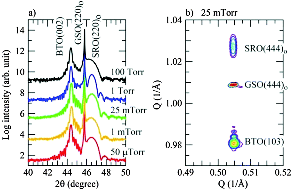 | ||
| Fig. 1 XRD study of various oxygen deficient BTO thin films: (a) 2θ–θ profiles for the BaTiO3−δ films grown under varying oxygen cooling conditions. (b) Semi-logarithmic contour plot of reciprocal space mapping around the (444)o GdScO3 (GSO) Bragg reflection for the 25 mTorr sample (similar RSM maps were obtained for other samples). The reflections from SRO and GSO are indexed using an orthorhombic unit cell. | ||
Current–voltage characteristics and resistive switching behaviour of BTO films were measured using an AIST-NT SmartSPM in c-AFM mode. Electrical bias was applied through the sample with the tip grounded for all the measurements as shown in Fig. 2. With the start and the end of the bias sweep set to 0 V, by sweeping the bias from negative to positive, typical current–voltage (I–V) characteristics of the as-fabricated BTO films cooled under different oxygen cooling pressures are shown in the top panels in Fig. 2a. As can be seen, the I–V characteristics are strongly dependent on the oxygen cooling pressure. Very low current of few pA just above the detection limit (∼0.2 pA) is observed for the film cooled under the largest pressure (100 Torr, see also ESI†) as shown in Fig. S2 (ESI†) and similar properties are seen for samples cooled under an oxygen pressure of 1 Torr and larger. For samples cooled at lower oxygen pressures the current under negative bias is drastically increased. By comparing the current of each sample read at the end voltages during the sweep, we find a close relationship between the electrical conductivity and the after-growth oxygen cooling pressure, considering that the conductivity of the film cooled at 50 μTorr is substantially enhanced with its current read at −8 V being more than 4 orders of magnitude greater than that of the sample cooled at 100 Torr. These results show a clear relationship between the overall conductivity of the film and the oxygen cooling pressure and provide a clue to control the electronic properties of BaTiO3−δ. We attribute the conduction mechanism to oxygen vacancies created within the films from the after-growth cooling process. However, quantitative determination of the oxygen vacancy concentration in the films was difficult because the film's resistance (along the in-plane direction) was too large and this did not allow for Hall resistivity measurements. Raman analysis could potentially be employed to see the structural and compositional changes for characterising the variation of oxygen vacancies although quantitative evaluation is still uncertain in our system.42 Nonetheless, the AFM based I–V curves exhibit a clear rectifying characteristic and hysteretic behaviour with two different reading currents at the same voltage for the up and down bias sweeps,43 therefore representing two resistance states, which have been observed before in c-AFM measurements on ferroelectric oxides.44 As seen in the middle and bottom panels of I–V curves, poled by +8 and −8 V, respectively, in Fig. 2, the electrical conductivity can be modulated by an electric field such that the positive bias switches the BTO film to a low resistance state (LRS), whereas the negative bias reversely switches the BTO back to a high resistance state (HRS). Regardless of poled states however, the current is found to start increasing at around 1.3 V (current onset, i.e. current above the detection limit (∼0.2 pA) of the c-AFM setup). In fact, the observation of rectifying characteristics suggests the formation of interfacial barriers in the system.
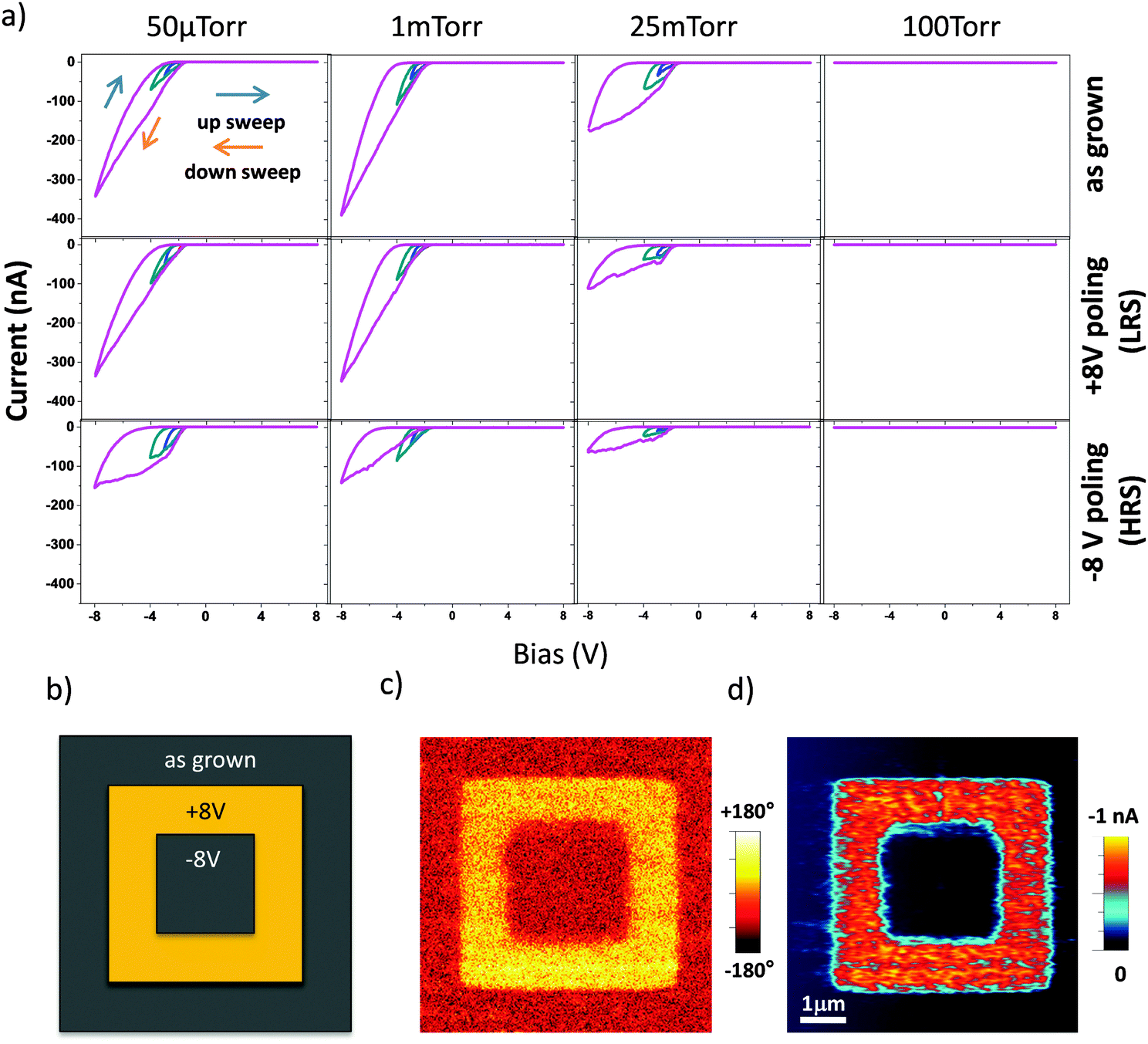 | ||
| Fig. 2 PFM and c-AFM study of various BTO films. (a) Locally acquired I–V curves of resistive switching behaviour for various BTO films in the as-grown and different pre-poled areas with I–V end-voltages of −3 V (blue), −4 V (green), and −8 V (violet). (b) Schematic of applied poling voltages for BTO films. (c and d) Piezoresponse (PFM) phase image indicating ferroelectric polarization in the +8 V area has been switched (polarization: yellow-up, brown-down) and the c-AFM image at −2 V bias (low bias) showing resistive switching behaviour of the poled area for the 50 μTorr sample. | ||
To further analyse the electrical behaviour of the samples, the current–voltage curves are plotted on a semi-logarithmic scale and a representative log I–V curve of the 50 μTorr sample is shown in the ESI† (Fig. S3). The I–V curves in the low voltage region for both the LRS and the HRS during the up- and down-sweeps, respectively, are well-fitted to a straight line. This result agrees with a basic Schottky barrier conduction model, meaning that the thermionic emission process is predominant. The ideality factors, n, of the LRS and the HRS based on the I–V curves by using a thermionic emission model are roughly 5 and 11, respectively, for the sample cooled at 50 μTorr (see ESI†). While this is much larger than the ideal value of 1 in a semiconductor Schottky junction, such a large ideality factor has been reported in other switchable diodes45 and the metal/porous-Si/Si diodes.46 In the case of the metal/porous-Si/Si diode, the rectifying behaviour stems from the band bending inside the Si layer at the interface, and the porous Si layer acts as a barrier to the carrier conduction. The large series resistance due to the porous-Si layer results in the large ideality factor of the metal/porous-Si/Si diode. With this in mind, the large n values in our samples can be attributed to an additional barrier layer that may form between the tip and BaTiO3−δ. Further work by cross-sectional TEM characterisation can be used to observe this additional layer.47 Considering that the thermionic emission process dominates the conduction mechanism in the probed region, the resistive switching behaviour of BTO films is attributable to Schottky barrier modulation with oxygen vacancy migration. For example, the larger current in the LRS is due to a reduced barrier height with a larger distribution of oxygen vacancies with respect to the HRS. This observation indicates that oxygen vacancies in the BTO films, which provide electronic carriers, play an important role in the observed electronic properties of the material.
In order to understand and visualize the conductivity after switching with different set-voltages, we pre-poled the films in micron sized areas as shown schematically in Fig. 2b. Piezoresponse (PFM) and c-AFM images after pre-poling are acquired for the 50 μTorr. Fig. 2c shows that the ferroelectric polarization has been switched in the area where +8 V was applied and switched back to the inner area with −8 V bias. Such ferroelectric switching behaviour is observed by PFM scans in all of the BTO films. Increased conductivity is seen during the c-AFM scan at a “read” bias voltage of −2 V in Fig. 2d. The region with polarization reversal to the downward direction remains highly conductive in comparison to the as-grown region and the region poled with −8 V. After applying a poling voltage of around ±3 V in a 4-by-4 μm2 area, exceeding the coercive voltage, the switching of ferroelectric domains is observed with a clear phase contrast (∼180°). In fact, this minimal voltage required for the ferroelectric switching is much greater than the observed onset voltage range for the current in the I–V curves during the bias down-sweep in Fig. 2. We also compared the onset voltages of current flow between the samples grown at different cooling oxygen pressures and poling states, however, no clear relationship was found. It is important to note that in the I–V curves there is no apparent change in current associated with the ferroelectric switching around its coercive voltage. These observations indicate that while the data in Fig. 2c and d would suggest a correlation between the ferroelectric polarization direction and the current, the contribution of polarization reversal to the change in electrical conductivity is rather small. Instead, we can explain the resistive switching mechanism in terms of the distribution of oxygen vacancies along with modulation of interfacial barriers. In our system, the nano-capacitor structure, consisting of diamond tip/BaTiO3−δ/SRO suggests the formation of a Schottky-like barrier, considering the rectifying I–V characteristics and the bias direction. However, the interface of BaTiO3−δ/SRO is reported to form a Schottky barrier that can be modulated by ferroelectric polarization, resulting in hysteretic and rectifying characteristics.48 Provided that the oxygen vacancies are positive charge carriers that can be tuned by electrochemical interactions,49 the application of the positive bias accumulates the oxygen vacancies near the top surface and leads to a highly conductive surface layer (with low-valence Ti), resulting in the LRS, while the applied negative bias dispreads the vacancies from the surface region and forms an insulating surface layer (with high-valence Ti), resulting in a HRS, as shown in Fig. 3. With this in mind, the interfacial effect at the diamond tip/BaTiO3−δ interface should dominate the conduction mechanism. Therefore, the bias dependent oxygen vacancy movement should play a decisive role in the resistance switching in the oxygen deficient BTO films. In fact, this bias-dependent oxygen vacancy movement, in turn, results in the modulation of the local resistance.50
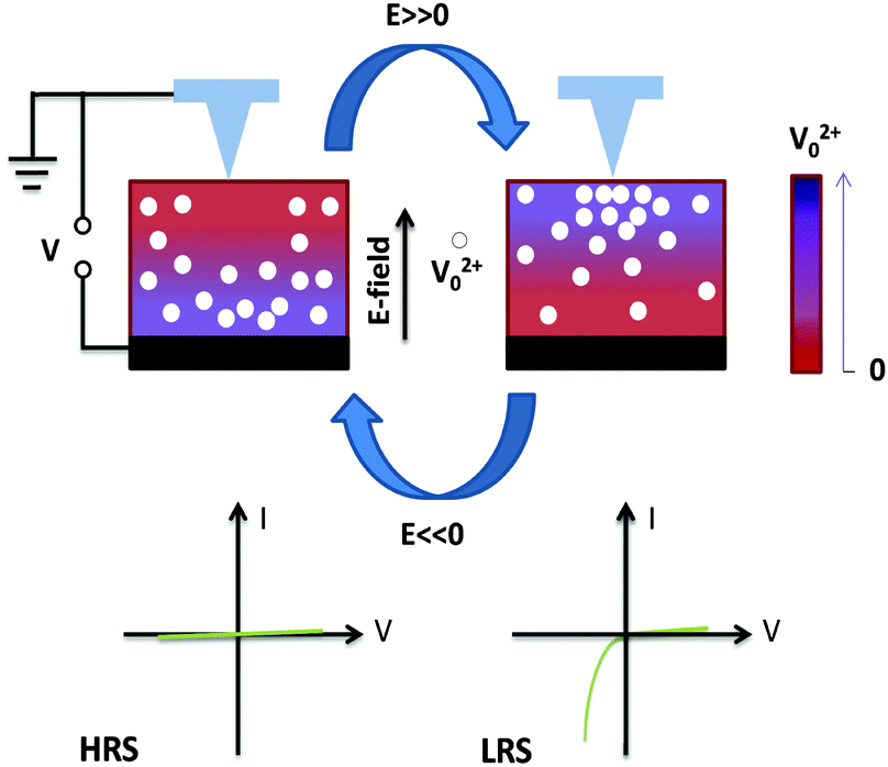 | ||
| Fig. 3 The mechanism of the bias-dependent movement of oxygen vacancies. Schematic diagram illustrating the electric field dependent movement of oxygen vacancy (V2+O), which results in the change in the distribution of the V2+O content in BaTiO3−δ films. Oxygen vacancies are spontaneously produced during the sample cooling process and respond to the electric field because the oxygen vacancies are positively charged. In a positive field (from the bottom to top directional field), oxygen vacancies are moving upward and accumulating near the top surface. By applying the opposite bias voltage, and thus the negative electric field, the oxygen vacancies can be dispersed from the top surface. Consequently, I–V curves are dependent on the oxygen vacancy content that can be tuned by the bias voltage. | ||
We also measured I–V curves over a long period of time to directly see the impact of oxygen vacancies on the conductivity and the observed resistive switching properties. At the early stages after thin film fabrication, we observed clear rectifying and hysteretic characteristics of I–V curves, however no measurable current was found after an 8 month period of time due to the re-oxygenation of the thin film samples under ambient conditions and the associated removal of oxygen vacancies. A representative comparison result of all BTO films is shown in the ESI† (Fig. S4). However, if the BTO films are deposited with suitable top electrodes41 rather than a conductive AFM tip, oxygen vacancies could potentially be captured within the film and retained for prolonged resistive switching characteristics. Further investigations by implementation of top electrodes are needed in this system. In order to clarify these resistive switching properties, we carried out I–V curve measurements for different poling histories of the investigated material, as shown in Fig. 4a. (a): (i) Normal I–V curve (−4 V → +4 V → −4 V), (ii) I–V curve (−4 V → +4 V → −4 V) after taking an I–V curve (0 V → +8 V), and (iii) I–V curve (−4 V → +4 V → −4 V) after taking an I–V curve (0 V → −8 V). These I–V curves show that the highest current is seen after a bias sweep from 0 to +8 V, whereas the lowest current is found after taking a bias sweep from 0 to −8 V. Our results clearly show, following the same trend as Fig. 2, that a highly positive pre-poling voltage increases the current levels, whereas the highly negative pre-poling voltage almost suppresses the current completely. Based on these results, we can consider that oxygen vacancies sufficiently move to or away from the surface under a high electric field, whereas the field-induced distribution of the vacancies is rather small under a low electric field. This indicates that a high electric field can function as a bias to control the oxygen vacancy distribution for switching between the HRS and the LRS whereas the low electric field can be used to read a current at a specific resistance state.
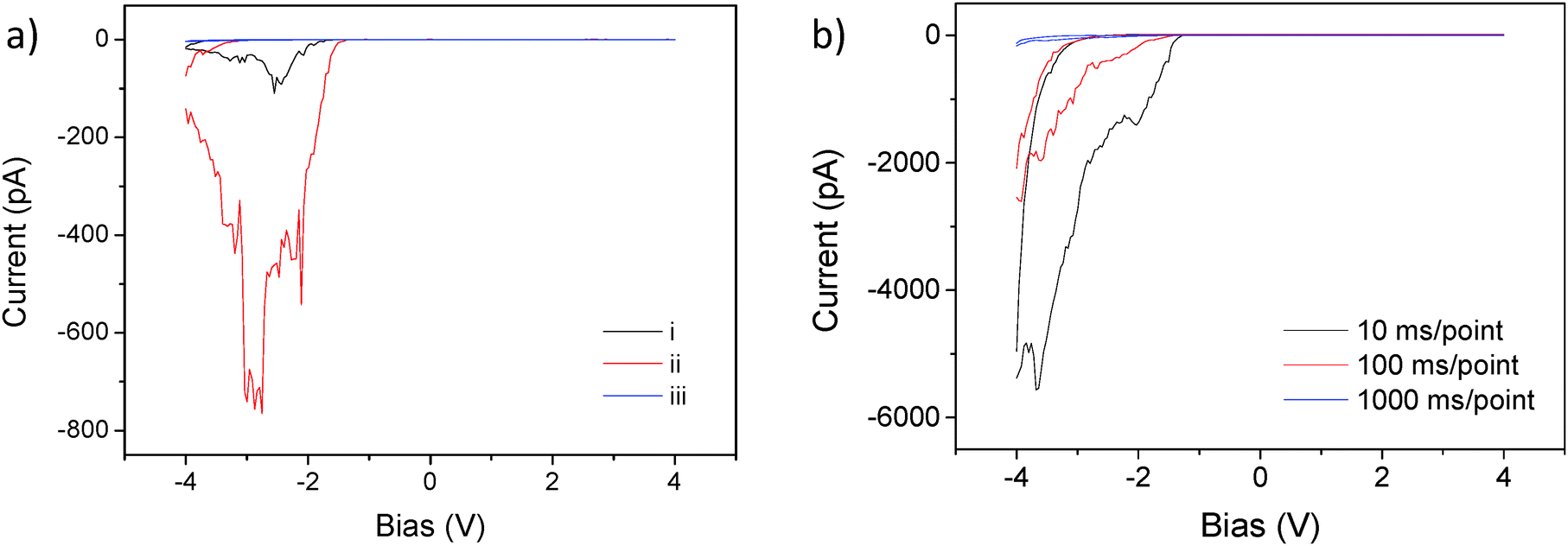 | ||
| Fig. 4 I–V curve measurements for different poling histories and time dependent studies of resistive switching behaviour for the 50 μTorr sample. (a) I–V curves for different poling histories at a ramping speed of 100 ms per point: (i) Normal I–V curve (−4 V to +4 V), (ii) I–V curve (−4 V to +4 V) after taking an I–V curve (0 V to +8 V), and (iii) I–V curve (−4 V to +4 V) after taking an I–V curve (0 V to −8 V). (b) I–V curves up to 4 V bias with different bias ramping speeds (200 points per curve) after pre-poling with +8 V. High speed (the 10 ms per point scan) retains increased current levels set by the pre-poling positive bias with +8 V while slow speeds show highly decreased current levels at −4 V due to neutralization of the pre-poling positive voltage. | ||
To further evaluate the resistance switching behaviour, we also investigated time-dependent conduction properties by measuring I–V curves over different time scales. Fig. 4b shows I–V curves up to 4 V bias with different bias ramping speeds (10, 100, and 1000 ms per point for 200 points per curve) for the sample cooled under 50 μTorr, with the most oxygen vacancies. Before taking I–V curves with different bias ramping speeds, the sample was poled with +8 V for switching it to the LRS. As a result, the current read at −4 V shows that a high speed scan (10 ms per point) retains the increased current set by the positive bias while a slow speed scan (1000 ms per point) shows the extremely decreased current set by the negative bias, indicating that the resistance switching can be induced by adjusting the period of the applied bias. This can be attributed to time-varying dynamics of oxygen vacancies, which are known to be mobile and movable with electric fields.51 Their diffusivity in certain perovskite oxides has been estimated to be of the order of 10−17 cm2 s−1 at room temperature.23 Our results offer promising aspects of resistive switching properties based on oxygen vacancies if strict control of the amplitude and the period of the applied bias can lead to solid switching behaviour with little fatigue. In order to test the repeatability of the resistive switching, we explored pulsed-voltage-induced resistive switching characteristics, using a built-in oscilloscope in our AFM system. Fig. 5 shows the resistive switching characteristics of the 50 μTorr sample. Pulsed bias voltages of ±8 V are used in order to switch between the high resistance state (HRS) and the low resistance state (LRS). After switching with ±8 V, −3 V is used as a “read” voltage to evaluate conductivity by measuring current. Fig. 5a shows the periodic resistive switching behaviour with pulsed bias voltages of ±8 V over a 120 second period. After switching with +8 V, currents measured at −3 V can be seen as a small trough and their average value is found to be around −100 pA. On the other hand, after switching with −8 V, current values read at −3 V show almost no measurable current and are below the noise floor of our c-AFM system (∼100 fA). Moreover, we calculated the resistance values using the measured currents at −3 V and plotted both values against the number of switching cycles. We found that the switching ratio (high resistance/low resistance) is greater than 103 as a lower limit based on mean HRS current values.
 | ||
| Fig. 5 Pulse-voltage mode resistive switching behaviour. (a) Repeatability of the resistive switching behaviour of the 50 μTorr sample, measured in the pulse-voltage mode. Pulsed bias voltages of ±8 V were, respectively, applied via a conductive AFM tip. Switching voltages were alternated with a period of roughly 10 seconds. Resistance values were evaluated from mean current values at V = −3 V. The sequence of the applied voltages is shown in red and the resultant currents are plotted in blue. (b) The measured currents (blue squares) and the corresponding resistance (red and black circles) as a function of the number of ±8 V bias voltage cycles. The current values were extracted from the plot in (a). Resistive switching of at least three orders of magnitude is observed (low resistance state LRS vs. high resistance state HRS). (c) Pulse mode measurements for long cycles of I–V curves for 50 μTorr BaTiO3−δ after additional heating under vacuum conditions. | ||
These results demonstrate the robustness of the bias-induced oxygen vacancy movements which are responsible for the switchable enhancement of the conductivity in BTO films as shown in Fig. 3 (vacancies move to the film surface or away from the film surface).23 To further evaluate the potential of our devices and test repeatability, we took long cycle pulsed mode measurements for testing the fatigue behaviour of resistive switching properties. We used a 50 μTorr BTO sample after heating it to 500 °C for 10 minutes under vacuum conditions. To perform a data retention test, we applied up to several 103 cycles of voltage stresses with a period of each cycle set to 8 seconds and an amplitude of Vp = ±8 V for switching between the LRS (+8 V) and the HRS (−8 V), while current levels were instantaneously measured at −3 V after switching. Our long time trace pulsed measurements show more than 5000 cycles of resistive switching properties with little fatigue as shown in Fig. 5c. In this case, the average switching ratio is found to be roughly ∼4500. After more than 6000 cycles, the BTO still exhibited resistive switching characteristics with reduced current read at the LRS while the current level at the HRS remained almost the same, thus giving a lower switching ratio. It is also interesting to note that the current level can be drastically modulated by the pulse duration time or the amplitude of the applied voltage, which in turn changes the switching ratio.
4. Conclusion
In summary, we have successfully deposited epitaxial oxygen deficient BaTiO3−δ thin films on SRO buffered GSO substrates by pulsed laser deposition and following an after-growth oxygen cooling process, unveiled the resistive switching characteristics of these films with regard to the underpinning mechanisms of such phenomena.11,52 These films show a clear resistive switching behaviour that is strongly dependent on the oxygen cooling pressures, resulting in the bias-induced modulation of oxygen vacancies in the system. Moreover, electrical poling can tune the resistance values by switching between the HRS and the LRS due to the bias dependent movement of oxygen vacancies with the aid of formation of interfacial barriers. From a device perspective, our results demonstrate promising aspects for the use of oxygen deficient oxides tuned by after-growth oxygen cooling pressure treatments with the ability to control resistive switching by an electric field. Further investigations are needed to develop these devices and improve the degradation of memory applications.Acknowledgements
We acknowledge support by the Australian Research Council through ARC Discovery Projects and a Future Fellowship. This work was also supported by the National Research Foundation of Korea funded by the Ministry of Education, Science, and Technology (contract no. NRF-2013S1A2A2035418). The work was also partially supported by the Japan Science and Technology Agency, CREST, a Grant-in-Aid for Scientific Research (Grant No. 24760009), and a grant for the Joint Project of Chemical Synthesis Core Research Institutions from the Ministry of Education, Culture, Sports, Science and Technology of Japan.References
- A. I. Kingon, J.-P. Maria and S. K. Streiffer, Nature, 2000, 406, 1032–1038 CrossRef CAS PubMed.
- Y. S. Kim, D. H. Kim, J. D. Kim, Y. J. Chang, T. W. Noh, J. H. Kong, K. Char, Y. D. Park, S. D. Bu, J.-G. Yoon and J.-S. Chung, Appl. Phys. Lett., 2005, 86, 102907 CrossRef.
- Y. W. Cho, S. K. Choi and G. V. Rao, Appl. Phys. Lett., 2005, 86, 202905 CrossRef.
- E. Y. Tsymbal and H. Kohlstedt, Science, 2006, 313, 181–183 CrossRef CAS PubMed.
- A. Gruverman, D. Wu, H. Lu, Y. Wang, H. W. Jang, C. M. Folkman, M. Y. Zhuravlev, D. Felker, M. Rzchowski, C. B. Eom and E. Y. Tsymbal, Nano Lett., 2009, 9, 3539–3543 CrossRef CAS PubMed.
- V. Garcia, S. Fusil, K. Bouzehouane, S. Enouz-Vedrenne, N. D. Mathur, A. Barthelemy and M. Bibes, Nature, 2009, 460, 81–84 CrossRef CAS PubMed.
- M. Gajek, M. Bibes, S. Fusil, K. Bouzehouane, J. Fontcuberta, A. Barthelemy and A. Fert, Nat. Mater., 2007, 6, 296–302 CrossRef CAS PubMed.
- P. Maksymovych, S. Jesse, P. Yu, R. Ramesh, A. P. Baddorf and S. V. Kalinin, Science, 2009, 324, 1421–1425 CrossRef CAS PubMed.
- S. Q. Liu, N. J. Wu and A. Ignatiev, Appl. Phys. Lett., 2000, 76, 2749–2751 CrossRef CAS.
- A. Beck, J. G. Bednorz, C. Gerber, C. Rossel and D. Widmer, Appl. Phys. Lett., 2000, 77, 139–141 CrossRef CAS.
- Y. Watanabe, J. G. Bednorz, A. Bietsch, C. Gerber, D. Widmer, A. Beck and S. J. Wind, Appl. Phys. Lett., 2001, 78, 3738–3740 CrossRef CAS.
- A. Sawa, T. Fujii, M. Kawasaki and Y. Tokura, Appl. Phys. Lett., 2004, 85, 4073–4075 CrossRef CAS.
- T. W. Hickmott, J. Appl. Phys., 1962, 33, 2669–2682 CrossRef CAS.
- I. G. Baek, M. S. Lee, S. Seo, M. J. Lee, D. H. Seo, D. S. Suh, J. C. Park, S. O. Park, T. I. Kim, I. K. Yoo, U. i. Chung and J. T. Moon, IEDM Technical Digest, 2004, 587–590 CAS.
- B. J. Choi, D. S. Jeong, S. K. Kim, C. Rohde, S. Choi, J. H. Oh, H. J. Kim, C. S. Hwang, K. Szot, R. Waser, B. Reichenberg and S. Tiedke, J. Appl. Phys., 2005, 98, 033715 CrossRef.
- K. Kinoshita, T. Tamura, M. Aoki, Y. Sugiyama and H. Tanaka, Appl. Phys. Lett., 2006, 89, 103509 CrossRef.
- D. B. Strukov, G. S. Snider, D. R. Stewart and R. S. Williams, Nature, 2008, 453, 80–83 CrossRef CAS PubMed.
- R. Waser and M. Aono, Nat. Mater., 2007, 6, 833–840 CrossRef CAS PubMed.
- A. Baikalov, Y. Q. Wang, B. Shen, B. Lorenz, S. Tsui, Y. Y. Sun, Y. Y. Xue and C. W. Chu, Appl. Phys. Lett., 2003, 83, 957–959 CrossRef CAS.
- L. Esaki, R. B. Laibowitz and P. J. Stiles, IBM Technical Disclosure Bulletin, 1971, 13, 2161 Search PubMed.
- P. W. M. Blom, R. M. Wolf, J. F. M. Cillessen and M. P. C. M. Krijn, Phys. Rev. Lett., 1994, 73, 2107–2110 CrossRef CAS PubMed.
- A. Schmehl, F. Lichtenberg, H. Bielefeldt, J. Mannhart and D. G. Schlom, Appl. Phys. Lett., 2003, 82, 3077–3079 CrossRef CAS.
- R. Meyer, J. R. Contreras, A. Petraru and H. Kohlstedt, Integr. Ferroelectr., 2004, 64, 77–88 CrossRef CAS.
- L. Pintilie, V. Stancu, L. Trupina and I. Pintilie, Phys. Rev. B: Condens. Matter Mater. Phys., 2010, 82, 085319 CrossRef.
- M. P. Singh, L. Méchin, W. Prellier and M. Maglione, Appl. Phys. Lett., 2006, 89, 202906 CrossRef.
- S. Y. Wang, M. Li, W. F. Liu and J. Gao, Phys. Lett. A, 2015, 379, 1288–1292 CrossRef CAS.
- S. C. Chae, J. S. Lee, S. Kim, S. B. Lee, S. H. Chang, C. Liu, B. Kahng, H. Shin, D.-W. Kim, C. U. Jung, S. Seo, M.-J. Lee and T. W. Noh, Adv. Mater., 2008, 20, 1154–1159 CrossRef CAS.
- J. J. Yang, M.-X. Zhang, J. P. Strachan, F. Miao, M. D. Pickett, R. D. Kelley, G. Medeiros-Ribeiro and R. S. Williams, Appl. Phys. Lett., 2010, 97, 232102 CrossRef.
- J. J. Yang, D. B. Strukov and D. R. Stewart, Nat. Nanotechnol., 2013, 8, 13–24 CrossRef CAS PubMed.
- M. D. Pickett, D. B. Strukov, J. L. Borghetti, J. J. Yang, G. S. Snider, D. R. Stewart and R. S. Williams, J. Appl. Phys., 2009, 106, 074508 CrossRef.
- D.-H. Kwon, K. M. Kim, J. H. Jang, J. M. Jeon, M. H. Lee, G. H. Kim, X.-S. Li, G.-S. Park, B. Lee, S. Han, M. Kim and C. S. Hwang, Nat. Nanotechnol., 2010, 5, 148–153 CrossRef CAS PubMed.
- J. P. Strachan, M. D. Pickett, J. J. Yang, S. Aloni, A. L. David Kilcoyne, G. Medeiros-Ribeiro and R. Stanley Williams, Adv. Mater., 2010, 22, 3573–3577 CrossRef CAS PubMed.
- J. Blanc and D. L. Staebler, Phys. Rev. B: Condens. Matter Mater. Phys., 1971, 4, 3548–3557 CrossRef.
- R. Waser, T. Baiatu and K.-H. Härdtl, J. Am. Ceram. Soc., 1990, 73, 1654–1662 CrossRef CAS.
- H.-I. Yoo, M.-W. Chang, T.-S. Oh, C.-E. Lee and K. D. Becker, J. Appl. Phys., 2007, 102, 093701 CrossRef.
- D. Kan and Y. Shimakawa, Appl. Phys. Lett., 2011, 99, 081907 CrossRef.
- J. Shin, S. V. Kalinin, A. Y. Borisevich, E. W. Plummer and A. P. Baddorf, Appl. Phys. Lett., 2007, 91, 202901 CrossRef.
- M. L. Scullin, J. Ravichandran, C. Yu, M. Huijben, J. Seidel, A. Majumdar and R. Ramesh, Acta Mater., 2010, 58, 457–463 CrossRef CAS.
- C. H. Yang, J. Seidel, S. Y. Kim, P. B. Rossen, P. Yu, M. Gajek, Y. H. Chu, L. W. Martin, M. B. Holcomb, Q. He, P. Maksymovych, N. Balke, S. V. Kalinin, A. P. Baddorf, S. R. Basu, M. L. Scullin and R. Ramesh, Nat. Mater., 2009, 8, 485–493 CrossRef CAS PubMed.
- C.-H. Yang, D. Kan, I. Takeuchi, V. Nagarajan and J. Seidel, Phys. Chem. Chem. Phys., 2012, 14, 15953–15962 RSC.
- A. Ikeda-Ohno, J. S. Lim, T. Ohkochi, C. H. Yang and J. Seidel, Phys. Chem. Chem. Phys., 2014, 16, 17412–17416 RSC.
- S.-L. Li, J. Li, Y. Zhang, D.-N. Zheng and K. Tsukagoshi, Appl. Phys. A: Mater. Sci. Process., 2011, 103, 21–26 CrossRef CAS.
- P. Maksymovych, J. Seidel, Y. H. Chu, P. Wu, A. P. Baddorf, L.-Q. Chen, S. V. Kalinin and R. Ramesh, Nano Lett., 2011, 11, 1906–1912 CrossRef CAS PubMed.
- J. Seidel, G. Singh-Bhalla, Q. He, S.-Y. Yang, Y.-H. Chu and R. Ramesh, Phase Transitions, 2012, 86, 53–66 CrossRef.
- T. Choi, S. Lee, Y. J. Choi, V. Kiryukhin and S.-W. Cheong, Science, 2009, 324, 63–66 CrossRef CAS PubMed.
- M. Ben-Chorin, F. Möller and F. Koch, J. Appl. Phys., 1995, 77, 4482–4488 CrossRef CAS.
- L. Song-Lin, Z. L. Liao, J. Li, J. L. Gang and D. N. Zheng, J. Phys. D: Appl. Phys., 2009, 42, 045411 CrossRef.
- Y. A. Park, K. D. Sung, C. J. Won, J. H. Jung and N. Hur, J. Appl. Phys., 2013, 114, 094101 CrossRef.
- J.-L. Gang, S.-L. Li, Z.-L. Liao, Y. Meng, X.-J. Liang and D.-M. Chen, Chin. Phys. Lett., 2010, 27, 027301 CrossRef.
- A. Sawa, Mater. Today, 2008, 11, 28–36 CrossRef CAS.
- J. Seidel, W. Luo, S. J. Suresha, P. K. Nguyen, A. S. Lee, S. Y. Kim, C. H. Yang, S. J. Pennycook, S. T. Pantelides, J. F. Scott and R. Ramesh, Nat. Commun., 2012, 3, 799 CrossRef CAS PubMed.
- J. Rodríguez Contreras, H. Kohlstedt, U. Poppe, R. Waser, C. Buchal and N. A. Pertsev, Appl. Phys. Lett., 2003, 83, 4595–4597 CrossRef.
Footnote |
| † Electronic supplementary information (ESI) available: AFM topography scans, fitting of I–V curves to the Schottky model and I–V curve measurements over a period of time. See DOI: 10.1039/c5cp05333a |
| This journal is © the Owner Societies 2016 |