Manipulating the voltage drop in graphene nanojunctions using a gate potential†
Abstract
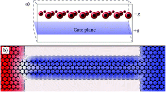
Graphene is an attractive electrode material to contact nanostructures down to the molecular scale since it can be gated electrostatically. Gating can be used to control the doping and the energy level alignment in the nanojunction, thereby influencing its conductance. Here we investigate the impact of electrostatic gating in nanojunctions between graphene electrodes operating at finite bias. Using quantum transport simulations based on density functional theory, we show that the voltage drop across symmetric junctions changes dramatically and controllably in gated systems compared to non-gated junctions. In particular, for p-type(n-type) carriers the voltage drop is located close to the electrode with positive(negative) polarity, the potential of the junction is pinned to the negative(positive) electrode. We trace this behaviour back to the vanishing density of states of graphene in the proximity of the Dirac point. Due to the electrostatic gating, each electrode exposes different density of states in the bias window between the two different electrode Fermi energies, thereby leading to a non-symmetry in the voltage drop across the device. This selective pinning is found to be independent of device length when carriers are induced either by the gate or dopant atoms, indicating a general effect for electronic circuitry based on graphene electrodes. We envision this could be used to control the spatial distribution of Joule heating in graphene nanostructures, and possibly the chemical reaction rate around high potential gradients.


 Please wait while we load your content...