Coupled optical absorption, charge carrier separation, and surface electrochemistry in surface disordered/hydrogenated TiO2 for enhanced PEC water splitting reaction†
Received
18th July 2015
, Accepted 4th February 2016
First published on 5th February 2016
Abstract
The central governing factors that influence the efficiency of photoelectrochemical (PEC) water splitting reaction are photon absorption, effective charge-carrier separation, and surface electrochemistry. Attempts to improve one of the three factors may debilitate other factors and we explore such issues in hydrogenated TiO2, wherein a significant increase in optical absorption has not resulted in a significant increase in PEC performance, which we attribute to the enhanced recombination rate due to the formation of amorphization/disorderness in the bulk during the hydrogenation process. To this end, we report a methodology to increase the charge-carrier separation with enhanced optical absorption of hydrogenated TiO2. Current methodology involves hydrogenation of non-metal (N and S) doped TiO2 which comprises (1) lowering of the band gap through shifting of the valence band via less electronegative non-metal N, S-doping, (2) lowering of the conduction band level and the band gap via formation of the Ti3+ state and oxygen vacancies by hydrogenation, and (3) material processing to obtain a disordered surface structure which favors higher electrocatalytic (EC) activity. This design strategy yields enhanced PEC activity (%ABPE = 0.38) for the N–S co-doped TiO2 sample hydrogenated at 800 °C for 24 h over possible combinations of N–S co-doped TiO2 samples hydrogenated at 500 °C/24 h, 650 °C/24 h and 800 °C/72 h. This suggests that hydrogenation at lower temperatures does not result in much increase in optical absorption and prolonged hydrogenation results in an increase in optical absorption but a decrease in charge carrier separation by forming disorderness/oxygen vacancies in the bulk. Furthermore, the difference in double layer capacitance (Cdl) calculated from electrochemical impedance spectroscopy (EIS) measurements of these samples reflects the change in the electrochemical surface area (ECSA) and facilitates assessing the key role of surface electrochemistry in PEC water splitting reaction. Additionally, we observed a blue-shift of the absorption spectrum and a decrease in both electrochemical (EC) and photoelectrochemical (PEC) activities after the removal of surface layers through focused ion beam (FIB) sputtering suggesting the importance of surface defects and photon absorption.
1. Introduction
Recently, black hydrogenated titania was reported to enhance photocatalytic performance by creating surface disorderness that helps in improving visible light absorption.1 Furthermore, the surface defects (oxygen vacancies/Ti3+ states) created upon amorphization will enhance the electrical conductivity which is essential for wide band gap materials like TiO2.1–8 Therefore, stabilization of surface defects is essential for better utilization of TiO2 material for photocatalytic applications in the long run. However, the stabilization of these defects is challenging and control of these oxygen vacancies is highly difficult as they depend on parameters such as temperature, surface states and synthesis conditions. Recently, Lin et al. made an attempt to make better utilization of surface defects by addition of dopants to the surface disordered TiO2 material.4 They synthesized oxygen deficient TiO2−x by hydrogenation followed by post-doping of non-metals (H, N, and I) and observed enhanced activity in photocatalytic H2 generation which is attributed to reduction in surface defects due to doping. The formation of surface defects can be further controlled by predoping of the non-metal during the synthesis of TiO2 followed by controlled hydrogenation. In the proposed methodology, we have done non-metal (N and S) doping followed by hydrogenation. Since the dopants (N and S) chosen in this methodology are less electro-negative in comparison to oxygen, lower is the energy required for hydrogen to remove these dopants (than oxygen) and create/stabilize the anion vacancies. We optimized the hydrogenation temperature and time (800 °C and 24 h) such that hydrogen diffuses on the surface but not to the bulk (lower hydrogenation temperature and time result in the hydrogenation of the surface and higher hydrogenation temperature and time result in the hydrogenation of the bulk). In this methodology, anion vacancies are predominantly present on the surface rather than in the bulk which reduce the charge carrier recombination and the element doped in the bulk increases the absoprtion cross-section.
To this end, we report the synthesis of N–S co-doped TiO2 followed by hydrogenation for enhanced PEC water splitting. In these doped hydrogenated TiO2 nanostructures, interaction of trapped electrons in oxygen vacancies (VO) present on the surface with adjacent Ti4+ centers leads to the formation of Ti3+ states. These electronic levels form below the conduction band and contribute to the enhanced optical absorption cross-section.9 Further, the electrochemical and photoelectrochemical properties of these doped hydrogenated TiO2 nanostructures will be improved due to the following reasons: (1) the presence of under co-ordinated or strained bonds on the surface helps in increasing electrocatalytic properties10–13 and (2) the synergestic effect between the added dopant and hydrogen passed to the system will stabilize the oxygen vacancies and improve the performance.14–18
In this work, we report (1) multi-element (N–S) doped hydrogenated TiO2 nanostructures fabricated on a stainless steel (SS) substrate via “click” chemistry for enhanced PEC water splitting reaction and (2) the role of surface defects (oxygen vacancies/Ti3+ states) in the amorphous layer of hydrogenated TiO2 material in charge-carrier transport. Nitrogen and sulphur are chosen as dopants as they are less electronegative than oxygen and expected to reduce the band-gap by introducing electronic states above valence band (VB) levels of TiO2 upon substitutional doping. Furthermore, hydrogenation will lead to stabilization of Ti3+ states which is expected to lower the band gap through lowering of the conduction band and also help in achieving amorphization of the surface layer which will lead to increased electrocatalytic properties. From EC/PEC measurements, it is observed that doped hydrogenated TiO2 nanostructures perform better than unhydrogenated undoped/doped and hydrogenated undoped TiO2 nanostructures, indicating the importance of the combined effect of doping and hydrogenation. The calculated efficiency metrics of the hydrogenated N–S co-doped TiO2@800 °C/24 h sample yields an applied bias photon to current conversion efficiency (ABPE) of 0.38%@0.63 V applied bias, an intrinsic solar to chemical conversion (ISTC) efficiency of 0.031 (or 3.1%)@1.27 V vs. RHE (reversible hydrogen electrode) and an electrical and solar power-to-hydrogen conversion (ESPH) efficiency of 6.6%@1.56 V applied bias, respectively, which is higher than undoped/doped TiO2 nanostructures hydrogenated at different temperatures and time periods. The enhancement in PEC performance in doped hydrogenated TiO2 is attributed to the combined effect of doping, oxygen vacancy states, and Ti3+ states. We note that the 24 h hydrogenated sample possesses a higher bandgap (∼2.95 eV), but shows enhanced efficiency in comparison to the 72 h hydrogenated sample (∼2.94 eV). Though, there is no significant difference in the optical bandgap measured from Tauc plots of 24 h and 72 h hydrogenated samples, a noticeable difference in double layer capacitance (Table S6b, ESI†) is observed. This suggests the changes in the electrochemical surface area (ECSA) available for electrochemical reaction, which signifies the prominent role of surface electrochemistry in PEC water splitting reaction. Furthermore, the interfacial kinetics of surface disordered TiO2 nanostructures calculated from electrochemical impedance spectroscopy (EIS) studies under light illumination also show that optical absorption and charge carrier separation are not mutually exclusive pathways in enhancing the PEC performance of surface disordered/hydrogenated TiO2 and it is not enough to just increase optical absorption while trying to increase the PEC efficiency, but increase of PEC efficiency requires a finer balance of optimizing optical absorption without severely debilitating electron–hole separation. The role of the disordered surface generated due to hydrogenation in enhancing PEC activity is demonstrated by the removal of a few surface atomic layers from doped hydrogenated TiO2 nanostructures by focused ion beam (FIB) sputtering upon which a decrease in both EC/PEC activity and photon absorption cross-section in comparison to the un-sputtered sample is observed. This result gives credence to the need for disordered surfaces in TiO2 for obtaining enhanced PEC performance.
2. Experimental section
2.1 Synthesis of undoped and doped TiO2 nanoparticles
Titanium(IV) iso-propoxide (TTIP, 9 ml) was added dropwise into a homogeneous mixture of ethanol (150 ml) and water (9.75 ml). The reaction mixture was kept at 85 °C for 4 h under agitation followed by evaporation of ethanol. The sample was dried at 60 °C for 30 min to get TiO2 nanopowder which was finely ground and calcined at 400 °C for 3 h to yield the anatase TiO2 phase.21 For the synthesis of doped TiO2 nanoparticles, different precursor salts/solutions were used for different dopants. Nitrogen doping was achieved by addition of 5 ml of aq. NH3 solution. Similarly, a solution of 9.3 g of thiourea in 3.75 ml of DI water was used as a precursor for sulphur doping. For N–S co-doped TiO2 nanoparticle synthesis, a mixture of 2.5 ml of aq. NH3 and 5.4 g of thiourea was used as precursor solution. The above-mentioned experimental protocol for undoped TiO2 was followed except for the addition of the respective precursor salt/solution before the addition of TTIP to the ethanol–water mixture.
2.2 Hydrogenation of undoped/doped TiO2 nanoparticles
Calcined samples (undoped and doped TiO2 nanoparticles) were pelletized and hydrogenated at different temperatures in a range of 500 °C to 800 °C for 24 h and 72 h at 20 bar pressure in the hydrogenation chamber. The digital photograph of the reactor used for the hydrogenation process is shown in Fig. S1a (ESI†). It is also important to eliminate the possibility of “blackness” in TiO2 due to carbon intercalation, which is not easy to remove because of reducing hydrogenation conditions. In the present study, the possibility of carbon induced blackness was eliminated by a careful XPS study. We note that reaction conditions have to be maintained precisely to reproduce the results.
2.3 Fabrication of nanostructured TiO2 electrodes
Scheme 1 shows a schematic representation of the synthesis of hydrogenated N–S co-doped TiO2 nanostructures followed by clicking onto an alkyne functionalized stainless steel (SS) substrate using click chemistry. It involves four steps: (1) synthesis of doped TiO2 nanostructures; (2) hydrogenation of doped TiO2 nanostructures at various temperatures (500 °C, 650 °C, and 800 °C) and time periods (24 h and 72 h); (3) surface functionalization of TiO2 nanostructures with the azide group (Section 1.2, ESI†); (4) surface functionalization of the SS substrate with the alkyne group (Section 1.3, ESI†) respectively; and (5) coating of TiO2 nanostructures onto SS substrates via click chemistry (Section 1.4, ESI†).
 |
| | Scheme 1 Schematic representation of the synthesis and fabrication of hydrogenated N–S co-doped TiO2 nanostructures on an alkyne functionalized stainless steel (SS) substrate via click chemistry. | |
3. Results and discussion
3.1 Material characterization
3.1.1 XRD analysis.
XRD data of hydrogenated doped TiO2 nanostructures prepared at various temperatures and for different time durations are shown in Fig. 1a and Fig. S2 (ESI†). XRD data of samples hydrogenated at 500 °C for 24 h (i.e. hydrogenated anatase TiO2@500 °C/24 h, hydrogenated N-doped TiO2@500 °C/24 h, hydrogenated S-doped TiO2@500 °C/24 h, and hydrogenated N–S co-doped TiO2@500 °C/24 h) confirm the presence of the anatase phase with JCPDS card no: 00-004-0477 (Fig. 1 and Fig. S2b, ESI†). Up to the hydrogenation temperature of 650 °C, there is no appearance of the rutile phase as evident from the hydrogenated N–S co-doped TiO2@650 °C/24 h sample which shows a pure anatase phase (Fig. 1a). Further increase of hydrogenation temperature leads to the formation of the rutile phase as the major phase along with a small amount of anatase phase in hydrogenated N-doped TiO2@700 °C/24 h (Fig. S2b and c, ESI†), hydrogenated N–S co-doped TiO2@800 °C/24 h, and hydrogenated N–S co-doped TiO2@800 °C/72 h samples, respectively, (Fig. 1). The formation of a mixed phase is further supported by HRTEM/SAED analysis (Fig. 3 and 4). The N-doped, S-doped and N–S co-doped TiO2 nanostructures calcined at 400 °C possess crystallite sizes of ∼11.5 nm, 7.8 nm, and 4.2 nm, respectively, which are less than undoped TiO2 (∼17.7 nm) (Fig. S2a, ESI†). The decrease in the crystallite size of single element (N or S) and multi-element (N–S co-doped) TiO2 samples compared to un-doped TiO2 suggests dopant incorporation in the crystalline matrix.19,20 Furthermore, broadening of diffraction peaks of doped (N or S or N–S) TiO2 nanostructures in comparison with un-doped TiO2 nanostructures supports the modification of crystalline lattice parameters upon doping.
 |
| | Fig. 1 (a) XRD patterns and (b) Raman spectra of undoped TiO2 and hydrogenated N–S co-doped TiO2 samples. | |
3.1.2 Electron microscopy studies.
To study the morphology and subsequent changes in undoped/doped TiO2 nanostructures during the hydrogenation step, scanning electron microscopy (SEM) images were taken (Fig. 2, Fig. S3 and S4, ESI†). The N–S co-doped TiO2 sample hydrogenated at 500 °C temperature for 24 h shows irregular morphology with increased aggregation as compared to the non-hydrogenated sample (Fig. 2a). Furthermore, the same sample hydrogenated at elevated temperatures (650 °C and 800 °C) for 24 h/72 h shows larger clusters with irregular morphology (Fig. 2b–d). Therefore, it can be concluded that the surface morphology of multi-element doped TiO2 nanostructures enormously changes with increase in hydrogenation temperature. The amorphous TiO2 (uncalcined) and crystalline TiO2 (calcined) nanoparticles show spherical morphology with the size ranging from 110–160 nm (Fig. S3a and b, ESI†). N-doped and S-doped TiO2 nanoparticles also possess a spherical shape with the particle size of ∼100 ± 10 nm and 175 ± 10 nm, respectively, (Fig. S3c and d, ESI†). However, co-doping TiO2 with nitrogen and sulphur leads to anisotropic morphology (Fig. S3e, ESI†). Moreover, undoped/single element-doped (N or S) TiO2 samples hydrogenated at 500 °C for 24 h lead to an increase in the particle size compared to non-hydrogenated samples, while retaining spherical morphology (Fig. S4, ESI†). Additionally, the SEM image of N-doped TiO2 clicked over the SS substrate (Fig. S4d, ESI†) shows good surface coverage. Furthermore, EDAX analysis (Fig. S3f and Table S1, ESI†) confirms the presence of Ti and O elements along with dopants nitrogen (N) and sulphur (S). We believe that the photoefficiency can be further enhanced by the precise optimization of the dopant and hydrogenation conditions.
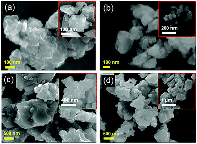 |
| | Fig. 2 SEM images of (a) hydrogenated N–S co-doped TiO2@500 °C/24 h; (b) hydrogenated N–S co-doped TiO2@650 °C/24 h; (c) hydrogenated N–S co-doped TiO2@800 °C/24 h; and (d) hydrogenated N–S co-doped TiO2@800 °C/72 h. | |
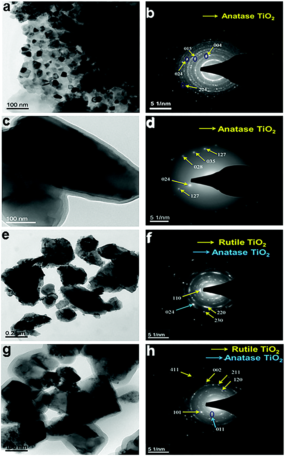
The morphology, crystallinity and formation of an amorphous layer upon hydrogenation have been further confirmed by transmission electron microscopy (TEM), high resolution transmission electron microscopy (HRTEM), and selective area electron diffraction (SAED) studies (Fig. 3 and 4, and Fig. S5, ESI†). TEM images of hydrogenated N–S co-doped TiO2@500 °C/24 h (Fig. 3a) and N–S co-doped TiO2@650 °C/24 h (Fig. 3c) show the particles with irregular morphology and the indexed SAED pattern (Fig. 3b and d) confirms the presence of the anatase phase which matches with XRD data (Fig. S2d, ESI†). Furthermore, N–S co-doped TiO2 samples hydrogenated at 800 °C for 24 h and 72 h also show irregular morphology (Fig. 3e and g) but possess both anatase and rutile crystalline phases. This is further supported by the indexed SAED pattern (Fig. 3f and h) and XRD data (Fig. 1a). Fig. 4 shows the HRTEM information of N-doped TiO2 hydrogenated at 700 °C for 24 h. The contrast in the TEM image clearly demarcates the rutile and anatase phases with lattice fringes (Fig. 4a). Furthermore, the HRTEM image (Fig. 4b) confirms the formation of a disordered/amorphous layer over the crystalline core with a thickness of ∼0.5 nm, which indicates that hydrogenation has created the surface defects (Fig. 4b) in the TiO2 material. The calculated d-spacing values of 0.1462, 0.2313 and 0.2145 nm correspond to the anatase phase and (130), (200), (111) planes correspond to rutile phases respectively (Fig. 4b). Furthermore, Fig. S5 (ESI†) shows the TEM images and the SAED pattern of crystalline TiO2 and N-doped TiO2 hydrogenated at 500 °C for 24 h. TEM images (Fig. S5a and c, ESI†) of both samples show particles with an irregular shape and SAED indexed patterns (Fig. S5b and d, ESI†) show the pure anatase phase.
 |
| | Fig. 3 TEM images of N–S co-doped TiO2 hydrogenated at temperatures of (a) 500 °C; (c) 650 °C; and (e) 800 °C for 24 h; and (g) at 800 °C for 72 h; (b), (d), (f) and (h) show the corresponding SAED patterns. | |
 |
| | Fig. 4 HRTEM image of the hydrogenated N-doped TiO2@700 °C/24 h sample showing (a) anatase–rutile phase interfaces and (b) the amorphous layer over the crystalline core. | |
3.1.3 Raman spectral analysis.
Raman spectra of undoped, doped, and hydrogenated doped samples are shown in Fig. 1b and Fig. S6 (ESI†). Raman spectra of unhydrogenated undoped/doped samples (Fig. S6a, ESI†) depict four major intense peaks observed at 143 cm−1, 395 cm−1, 513 cm−1 and 639 cm−1, attributed to the Eg, B1g, A1g + B1g, and Eg bands of the anatase phase of TiO2 respectively. Furthermore, hydrogenated TiO2@500 °C/24 h, hydrogenated N-doped TiO2@500 °C/24 h, hydrogenated S-doped TiO2@500 °C/24 h, hydrogenated N–S co-doped TiO2@500 °C/24 h, and hydrogenated N–S co-doped TiO2@650 °C/24 h possess anatase bands (Fig. S6b, ESI,† and Fig. 1b) which confirm that the anatase crystalline phase is consistent with XRD data (Fig. S2b, ESI†). However, N–S co-doped TiO2@800 °C/24 h and N–S co-doped TiO2@800 °C/72 h samples show three peaks located at ∼234 cm−1, 443 cm−1, and 610 cm−1, attributed to B1g, Eg, and A1g bands of the rutile TiO2 phase respectively, which is consistent with its XRD data (Fig. 1a). Furthermore, N-doped TiO2@700 °C/24 h possess both anatase and rutile bands indicating the formation of both anatase and rutile crystalline phases, which is consistent with its XRD data (Fig. S2b, ESI†). Additionally, a small shift along with broadening of the peak is observed at 141 cm−1 (Eg) (attributed to both anatase and rutile phases) with N-doped hydrogenated TiO2@500 °C/24 h and N-doped TiO2@700 °C/24 h nanostructures in comparison to N doped TiO2 nanostructure (Fig. S6c, ESI†). Furthermore, the same observation is found for the hydrogenated N–S co-doped TiO2@650 °C/24 h sample (B1g) as shown in Fig. S6d (ESI†). The shift and broadening of the peak indicate the non-stoichiometry or reduction in the original symmetry of the TiO2 lattice due to surface disorder.21 Additionally, Raman spectra of the hydrogenated TiO2@500 °C/24 h sample show two peaks at 1339 cm−1 (D band) and 1606 cm−1 (G band), which are attributed to Ti–H vibrations or surface disorder defects created due to the presence of carbon, wherein D and G bands (which are due to the presence of carbon in the SS substrate) will also emerge at the same wavenumbers (Fig. S18a, ESI†).
3.1.4 FTIR analysis.
FTIR spectra of undoped/doped/hydrogenated TiO2 nanostructures are shown in Fig. S7 and S8, and Table S2 (ESI†). FTIR spectra (Fig. S8b, ESI†) of hydrogenated TiO2 nanostructures show reduction in –OH peak intensity in comparison to unhydrogenated nanostructures suggesting the reduction of –OH groups present in the TiO2 sample. The presence of dopants N and S in the TiO2 matrix is confirmed by Ti–S and Ti–N characteristic peaks as shown in Fig. S7c and d and Table S2 (ESI†). Furthermore, the peaks at ∼3645, 3670, and 3685 cm−1 of the hydrogenated S-doped TiO2@500 °C/24 h sample are attributed to the tetrahedral co-ordinated vacancies (Fig. S8a, ESI†).22 FTIR spectra of azide functionalized undoped/doped and doped-hydrogenated TiO2 particles show a peak at ∼2110 cm−1 (Fig. S7b, ESI†) which confirms the presence of the azide group on particles. Additionally, FTIR spectra of the alkyne functionalized SS substrate show a peak at ∼2156 cm−1 confirming the presence of an alkyne group (Fig. S8b, ESI†). All functionalized TiO2 nanostructures show the presence of strong –CH2 stretching vibrations at ∼2950 cm−1 confirming the surface modification. Furthermore, an increase in the contact angle (∼97.50°) in the case of the alkyne functionalized electrode (hydrophobic) compared to the bare SS substrate/electrode (∼60°) (Fig. S8c, ESI†), suggests the presence of a terminal alkyne moiety on the surface which matches with our earlier report.23
3.1.5 UV-Vis spectral analysis.
UV-Vis spectra of undoped/doped and hydrogenated doped TiO2 samples are shown in Fig. S9 (ESI†). The approximate band gaps of all TiO2 nanostructures calculated from Tauc plots (undoped/doped/hydrogenated doped TiO2) are summarized in Table S3 (ESI†). The decrement in the optical bandgap of doped and hydrogenated samples is clearly visualized with the color of samples (Fig. S1b–n, ESI†). Both amorphous (uncalcined) and crystalline (calcined) TiO2 samples show absorption bands at around 387 nm and 392 nm (Fig. S9a, ESI†) which correspond to the bandgaps of 3.66 eV and 3.46 eV, respectively, measured from the corresponding Tauc plots (Fig. S9b, ESI†). A red-shift in the absorption band is observed when the TiO2 matrix is doped. The measured band gaps for N-doped TiO2, S-doped TiO2 and N–S co-doped TiO2 are found to be ∼3.38 eV, 3.37 eV, and 3.09 eV respectively. The S dopant due to its lower electronegativity can shift the VB to more upward direction in comparison to the N dopant, although both seem to possess same absorption cross-sections. Furthermore, N-doping leads to the stabilization of Ti3+ states.14,24 For this reason, co-doping leads to lowering of the band-gap more than individual doping (S or N). Furthermore, absorption spectra of hydrogenated TiO2 nanostructures (Fig. S9c, ESI†) show a red-shift with less optical band gap compared to their unhydrogenated counterparts. This is attributed to the formation of mid-gap states between the CB and the VB due to hydrogenation and the formation of oxygen vacancy and Ti3+ states.
3.1.6 Electron paramagnetic resonance (EPR) analysis.
Ti3+ surface defects are quite different from oxygen vacancies (VO).19 It is to be noted that Ti3+ states will be generally formed by the reduction of Ti4+ in either of the two ways: (1) the Ti4+ ion receives photoelectrons usually by UV light absorption on the TiO2 surface. The electrons can be trapped and tend to reduce Ti4+ cations to Ti3+ states.19,20 (2) Ti4+ reduction to Ti3+ is usually accompanied by loss of oxygen from TiO2 surface. Similarly, oxygen vacancies (VO) are responsible for the formation of color (F) centers, as the electron pair remains trapped in the cavity (VO), upon loss of an oxygen atom from the surface of metal oxide.25 Electron paramagnetic resonance (EPR) spectra are used to confirm the presence of surface defects (oxygen vacancies/Ti3+ states) in the surface disordered/hydrogenated TiO2 sample. It is known that for paramagnetic materials containing ‘‘F-centers’’ or oxygen vacancies, the resonance at g = 2.004 is the most prominent and characteristic electron signal.26 Undoped TiO2 nanostructures show the g-values of ∼2.003–2.004 (Fig. S10a, ESI†), which is attributed to the existence of oxygen vacancies. Furthermore, N–S co-doped TiO2 samples hydrogenated at 500 °C, 650 °C, and 800 °C for 24 h result in additional peaks at g ∼ 1.996 to 1.999 along with a small shift in the original oxygen vacancy state (g ∼ 2.003–2.007) (Fig. S10b, e, and f, ESI†). The peak that emerged at g = 1.996 to 1.999 in these samples is attributed to Ti3+ states due to the interaction of H atoms and the Ti4+ state of TiO2 leading to the formation of Ti3+ states (eqn (1)).| | | O2− + 2Ti4+ + H2 → 2Ti3+ + H2O | (1) |
This observation clearly confirms the presence of oxygen vacancies and Ti3+ states upon hydrogenation which is consistent with earlier reports.21,27 Furthermore, the doped unhydrogenated TiO2 sample (N–S co-doped TiO2) also shows a characteristic signal closer to the g value of 1.997 indicating the presence of Ti3+ states (Fig. S10c and d, ESI†). Therefore, Ti3+ states are present along with oxygen vacancies before hydrogenation (i.e. in doping stage) which is consistent with previous reports.28 Although, it is highly difficult to demarcate the presence and the individual role of oxygen vacancies relative to Ti3+ states in the enhanced PEC performance of doped and hydrogenated TiO2 samples,29 we attempted to find out the relative change in the concentration of oxygen vacancies from Mott–Schottky plots (Fig. S11, ESI†).28,30 Since oxygen vacancies act as electron donors, an increase in the donor density can be attributed to the increase in the concentration of oxygen vacancies. The donor density can be calculated from the relation
| |  | (2) |
where
Nd is the donor density,
e0 is the electron charge,
C is the capacitance,
ε is the dielectric constant of TiO
2 (∼31 in the case of anatase TiO
2),
31ε0 is the permittivity of vacuum, and
V is the potential applied at the electrode. The calculated slopes from Mott–Schottky plots, for anatase TiO
2, hydrogenated N–S co-doped TiO
2@800 °C/24 h, and hydrogenated N–S co-doped TiO
2@800 °C/72 h are found to be 6.87 × 10
10 cm
4 F
−2 V
−1, 4.44 × 10
10 cm
4 F
−2 V
−1, and 4.34 × 10
10 cm
4 F
−2 V
−1 respectively. Furthermore, the donor densities of the anatase TiO
2, hydrogenated N–S co-doped TiO
2@800 °C/24 h, and hydrogenated N–S co-doped TiO
2@800 °C/72 h are calculated to be 0.66 × 10
20, 1.02 × 10
20, and 1.05 × 10
20 cm
−3 respectively. An increase in the donor density of hydrogenated N–S co-doped TiO
2@800 °C/72 h and hydrogenated N–S co-doped TiO
2@800 °C/72 h samples with respect to anatase TiO
2 suggests that there is an increment in the concentration of oxygen vacancies in doped hydrogenated samples (hydrogenated N–S co-doped TiO
2@800 °C/72 h, and hydrogenated N–S co-doped TiO
2@800 °C/24 h) over the undoped unhydrogenated sample (anatase TiO
2).
3.1.7 X-ray photoelectron spectroscopy (XPS) analysis.
X-ray photoelectron spectroscopy (XPS) reveals the presence of elements and the associated chemical bonds on the surface within few atomic layers of the material. Two peaks of Ti 2p3/2 (456.8 eV) and Ti 2p1/2 (462.7 eV) are observed for hydrogenated N–S co-doped TiO2@650 °C/24 h nanostructures (Fig. S12, ESI†), which confirms the presence of Ti3+ states (Ti4+ + e− → Ti3+). The observed binding energies of 284.05 eV, 162.5 eV, 232.6 eV, and 397.7 eV represent C 1s, S 2p, S 2s, and N 1s signals, respectively (Fig. S12a, ESI†). Furthermore, XPS measurements were taken at slow scan rates to magnify the Ti and O peaks. Two nearby peaks are observed at binding energies of ∼55.1 eV and 61.6 eV which correspond to Ti 3s states. Additionally, the O 1s peak can be resolved into two peaks at about 530.39 eV and 531.2 eV, wherein the peak at 530.39 eV is attributed to Ti–O–Ti groups on the surface and the broader peak at 531.2 eV can be attributed to Ti–OH (Fig. S12b and c, ESI†). These observations confirm the presence of dopants as well as the defect states in the TiO2 matrix. Furthermore, deconvoluted XPS spectra of hydrogenated N–S co-doped TiO2@800 °C/24 h nanostructures are shown in Fig. 5. Four peaks at 557.7 eV, 558.6 eV, 559.3 eV, and 564.6 eV were observed from deconvoluted XPS Ti 2p spectra. The peaks at 558.6 eV and 564.6 eV can be attributed to 2p3/2 and 2p1/2 of Ti4+ ion states (Fig. 5c), and peaks at 557.7 eV (Fig. 5d) and 559.3 eV (Fig. 5c) can be attributed to 2p3/2 and 2p1/2 of Ti3+ states, respectively, which confirm the presence of Ti3+ states and defect states in the TiO2 matrix (Fig. 5d) consistent with earlier reports.32–34
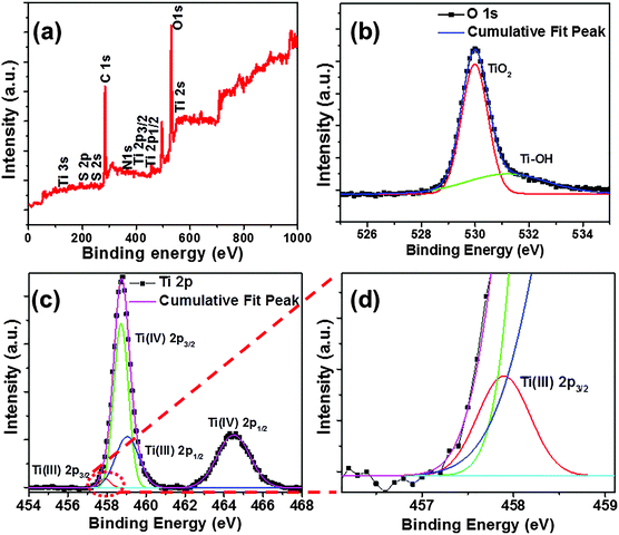 |
| | Fig. 5 XPS spectra of hydrogenated N–S co-doped TiO2@800 °C/24 h: (a) whole scan, (b) O 1s, (c) Ti 2p, and (d) the enlarged/resolved portion (red dotted lines of c) of the Ti 2p XPS peak. | |
We have performed XPS measurements to determine the valence band edge position of anatase TiO2 and hydrogenated N–S co-doped TiO2@800 °C/24 h samples (Fig. S13, ESI†). The calculated valence band edge position of anatase TiO2 is about 1.29 eV, whereas it is 0.86 eV in the case of the hydrogenated N–S co-doped TiO2@800 °C /24 h sample. This confirms the shift of the valence band edge position of the hydrogenated N–S co-doped TiO2@800 °C/24 h sample by 0.43 eV towards vacuum. Since the difference in the optical bandgap between anatase TiO2 and N–S co-doped TiO2@800 °C/24 h is about 0.51 eV, the rest of the fraction can be considered as a shift in the conduction band edge towards the valence band.
3.2 Electrochemical (EC)/photoelectrochemical (PEC) water splitting
The performance of fabricated nanostructures towards photoelectrochemical (PEC) water splitting is evaluated using both two-probe and three-probe methods.35 Current vs. applied bias/applied potential plots were recorded for all fabricated undoped/doped/hydrogenated doped TiO2 nanostructured electrodes in 2-probe (Fig. 6, Fig. S14, S15 and Table S4, ESI†) and 3-probe modes (Table S5, ESI†) in 0.1 M NaOH solution (pH ∼ 13.6). The observed onset working electrode potential of fabricated nanostructured electrodes is 0.52–0.6 V vs. Ag/AgCl (1.52–1.6 V vs. RHE) which corresponds to the oxygen evolution reaction (OER) potential. The best performance among all the prepared hydrogenated doped TiO2 samples is found to be for the hydrogenated N–S co-doped TiO2@800 °C/24 h sample with a current density of 6.3 mA cm−2 (under light) and 4.7 mA cm−2 (under dark) at 1.6 V applied bias, respectively, as measured in 2-probe mode (Fig. 6d). Furthermore, the same electrode shows current densities of 31.4 mA cm−2 (under light) and 25.6 mA cm−2 (under dark) in three-probe mode at a working electrode potential of 1.2 V vs. Ag/AgCl (2.2 V vs. RHE) applied potential (Table S5, ESI†). Two-probe measurements of undoped/doped/hydrogenated doped TiO2 nanostructured electrodes are shown in Fig. S14 and S15 (ESI†).
 |
| | Fig. 6 Current vs. applied bias plots of (a) N–S co-doped TiO2; (b) hydrogenated N–S co-doped TiO2@500 °C/24 h; (c) hydrogenated N–S co-doped TiO2@650 °C/24 h; (d) hydrogenated N–S co-doped TiO2@800 °C/24 h; (e) hydrogenated N–S co-doped TiO2@800 °C/72 h, and (f) the applied bias to photo-conversion efficiency (ABPE) of all N–S co-doped hydrogenated TiO2 samples performed in 0.1 M NaOH solution (two-probe measurements). | |
From Table S5 (ESI†), it is observed that hydrogenated TiO2 nanostructures show enhanced PEC activity in comparison to unhydrogenated TiO2 nanostructures. From the table, N doping in TiO2 improves EC activity but S doping does not. This can be rationalized from the fact that aliovalent N-doping leads to the formation of the Ti3+ state which helps in increasing EC activity. However, isovalent S-doping does not lead to the formation of any intermediate Ti3+ state, which contributes towards improvement in EC activity. Furthermore, due to less electronegativity of S, there would be less charge polarization over the Ti-atom which slightly lowers EC activity towards water splitting as evident from the lower EC activity of S-doped TiO2 in comparison to TiO2. However, co-doped TiO2 shows higher EC activity than both monodoped N- and S-doped TiO2 due to either a synergistic interplay of both dopants in enhancing the activity and/or improved electronic conductivity.36–38 It is also observed that all the hydrogenated samples show better EC activity in comparison to their unhydrogenated counterparts. This result implies that amorphization due to the hydrogenation process improves EC activity towards water splitting. However, EC activity of the hydrogenated samples significantly depends on the hydrogenation temperature which determines the crystalline phase. Among the co-doped hydrogenated TiO2 samples, the EC activity is found to be in the order of hydrogenated N–S co-doped TiO2@800 °C/24 h > hydrogenated N–S co-doped TiO2@800 °C/72 h > hydrogenated N–S co-doped TiO2@650 °C/24 h > hydrogenated N–S co-doped TiO2@500 °C/24 h. The increased EC activity of hydrogenated N–S co-doped TiO2@800 °C/24 h may be attributed to the synergistic effect of rutile and a small amount of anatase present in the sample. In this regard, it is pointed out that a mixed phase shows better EC activity in comparison to any single phase.39,40 However, an increase of the rutile phase beyond a percentage leads to a reduction in EC activity.41 Furthermore, the decrease in the dark current of the hydrogenated N–S co-doped TiO2@800 °C/72 h sample in comparison to the hydrogenated N–S co-doped TiO2@800 °C/24 h sample (Table S4, ESI†) may be attributed to the decrease in the electrochemical surface area (ECSA) upon hydrogenation for longer time (72 h), which is supported by a decrease in the double layer capacitance (Cdl) calculated from EIS circuits (Table S6b, Section 3.3, ESI†).
In order to compare the photo-performance of the electrodes, the applied bias photon to current conversion efficiency (ABPE) has been calculated using the following relation,
| |  | (3) |
where
jph is the photocurrent,
Vb is the applied bias between working and counter electrodes, and
Ptotal is the intensity of light (power) from a solar simulator. Since the photocurrent developed at low applied bias values play an important role in characterizing any photo material, we have taken the true activity of the photomaterial by measuring the applied bias to photo current conversion efficiency (ABPE), which signifies the minimum applied bias (below thermodynamic potential of water
i.e. 1.23 V), at which the maximum photon to current conversion is achieved.
42–44 The measured ABPE values of unhydrogenated and hydrogenated samples prepared at different temperatures and time periods are compared at 0.63 V and tabulated in Table S3 (ESI
†). Among all the prepared electrodes, the best ABPE value is found for the hydrogenated N–S co-doped TiO
2@800 °C/24 h sample with a value of ∼0.38%, at 0.63 V applied bias (
Fig. 6f). Therefore, the sample with the best photo activity performance in this work is hydrogenated N–S doped TiO
2@800 °C/24 h and is chosen based on the true ABPE value. We conclude from above values that hydrogenated undoped/doped TiO
2 nanostructures show better PEC performance than unhydrogenated nanostructures and we can attribute the enhanced performance to reduction in charge carrier recombination as well as an improvement in optical absorption with the proposed design strategy. From Table S3 (ESI
†), it is found that both N-doping and S-doping yield an enhancement of ABPE which can be ascribed to the enhancement of the photon absorption cross-section. Co-doping leads to a better ABPE value than any singular N- or S-doping (Fig. S16, ESI
†). The order of ABPE among co-doped hydrogenated TiO
2 samples is found to be N–S co-doped TiO
2@800 °C/24 h > hydrogenated N–S co-doped TiO
2@800 °C/72 h > hydrogenated N–S co-doped TiO
2@650 °C/24 h > hydrogenated N–S co-doped TiO
2@500 °C/24 h. The PEC activity in the disordered mixed phase is higher in comparison to the anatase phase.
40,41,45 It is evident from the above results that hydrogenation at higher temperature enhances the efficiency. It is to be noted that the 24 h hydrogenated sample with an optical bandgap of ∼2.95 eV shows enhanced efficiency in comparison to the 72 h hydrogenated sample having a bandgap of ∼2.94 eV. The reduction in the PEC performance of the 72 h hydrogenated sample over the 24 h hydrogenated sample can be attributed to (1) the decrease in the electrochemical surface area (ECSA) (Table S6b, ESI
†) as explained in Section 3.3, and (2) high charge carrier recombination that persists due to defect states/oxygen vacancies developed in bulk.
The PEC performance of the electrodes is also benchmarked by comparing the intrinsic solar to chemical conversion (ISTC) efficiency. This efficiency is calculated using three-electrode cell potentials (Fig. 7) which measure the maximum intrinsic power of the photo-anode to convert the solar light into chemical energy as per below relation,
| |  | (4) |
where photocurrent (
jphoto, difference in current density obtained with and without light at the same potential) is given in mA cm
−2, on the other hand, photovoltage
i.e. Vphoto is the difference in potentials under light (
Vlight) and dark (
Vdark) conditions at same current density. Furthermore, the maximum internal photovoltaic power of TiO
2 nanostructures is calculated from the plot between
jphoto and
Vphoto as shown in
Fig. 7b. For instance, under light illumination hydrogenated N–S co-doped TiO
2@800 °C/24 h shows the photocurrent of ∼0.58 mA cm
−2 at 1.45 V (
vs. RHE) whereas to obtain same current under dark conditions, this sample requires 1.48 V (
vs. RHE) which means that solar light provides energy that corresponds to the potential of 0.036 V or power of ∼0.021 mW cm
−2. As mentioned by Grätzel and co-workers, external power is saved as a result of the internal photovoltaic power of this sample which is calculated by the reduction in the water electrolysis conversion efficiency
i.e. 1.23 (
VRHE)/
Vdark,RHE = ∼82%. Thus, the ISTC efficiency of this sample is ∼0.82 × 0.021 = 0.0172 or 1.72% (
Fig. 7a). The maximum ISTC efficiency of ∼3.1% is obtained for hydrogenated N–S co-doped TiO
2@800 °C/24 h compared to other hydrogenated samples. The significance of ISTC can be further understood as follows; the maximum current density obtained at 1.45 V (
vs. RHE) with hydrogenated N–S co-doped TiO
2@800 °C/24 h is 0.775 mA cm
−2 which means that this electrode can produce the maximum chemical power of ∼0.953 mW cm
−2 and in this total power output, the internal solar conversion to the chemical power of hydrogenated N–S co-doped TiO
2@800 °C/24 h contributes ∼0.0172
i.e. 1.8% and the remaining power could be supplied from the external electrical energy. ISTC provides only half cell efficiency (as it is measured in three-electrode configuration) and does not include losses from other components of the PEC cell
i.e. the counter-electrode, electrolyte, wires
etc. Furthermore, both the efficiencies
i.e. ABPE and ISTC are mainly used to evaluate the performance of either PEC device or photoanode based on the photocurrent and photo-voltage. However, none of the above efficiencies provides the performance evaluation based on the total power output generated from the PEC device which is based on the total current density obtained due to contribution from applied bias and light. Hence, in order to do so, we propose a new efficiency metric called “electrical and solar power-to-hydrogen (ESPH)” which is based on the definition of efficiency
i.e. total power output divided by total power input.
 |
| | Fig. 7 (a) Intrinsic photovoltaic power characteristics; (b) intrinsic solar to chemical conversion (ISTC) efficiency; (c) micromoles of hydrogen production; and (d) the electrical and solar power-to-hydrogen (ESPH) conversion efficiency based on current and moles of hydrogen collected for the hydrogenated N–S co-doped TiO2@800 °C/24 h sample. | |
We measured ESPH for the hydrogenated N–S co-doped TiO2@800 °C/24 h electrode, which includes the external applied electrical power, along with solar power as the total power input.
| |  | (5) |
| |  | (6) |
During the water splitting reaction, oxygen and hydrogen gases were collected at working and counter-electrodes respectively. Evolved gases were observed to be in a stoichiometric ratio which suggests that there is no side product formation. The sample shows ESPH efficiencies of ∼1.18% and 7.2% at 0.63 and 1.56 V applied bias, respectively, which is the highest ESPH efficiency among all other samples (Fig. 7d). The possible reasons for lower ESPH efficiency are: (1) it is measured in a two-electrode configuration and gives full cell efficiency and (2) it includes all the parasitic losses that arise from different components of the PEC cell. Fig. 7c shows a plot of hydrogen collected during reaction vs. applied bias for the same sample under light illumination conditions. Furthermore, ESPH efficiency (based on moles of H2 production) under illumination (@ ∼1.56 V bias) for this sample is ∼5.83%. Additionally, we calculated the amount of hydrogen generated based on current density as well as based on collection as shown in Fig. 7c. The difference in ESPH as well as production of H2 based on current and moles of hydrogen collection can be attributed to the ohmic drop (IR drop) and other associated resistances during the collection of evolved gases using the “inverted beaker method” (Fig. S19, ESI†).
3.3 Electrochemical impedance spectra (EIS) analysis
The electrode/electrolyte interface kinetics and dynamics of electron transport of fabricated nanostructures can be analyzed using EIS analysis.46,47 We performed EIS measurements to investigate the conductivity and impedance values of the best sample “hydrogenated N–S co-doped TiO2@800 °C/24 h” on SS substrate under dark and light conditions (Fig. S17, ESI†); The experimental and simulated patterns match with the RS(R1C)(R2Q) circuit (inset image of Fig. S17a, ESI†), where RS represents the solution resistance of the electrolyte (i.e. ohmic resistance including the resistance of the electrolyte, separator and electrical contacts), C and Q being capacitance and constant phase element, and R1 and R2 being the resistances associated with the charge transfer process. The two semicircles correspond to the oxide/hydroxide covered mixed surface.48 The double layer charge capacitance (Cdl) vs. applied potential data for this sample is given in Table S6a (ESI†). Furthermore, a decrease in charge transfer resistance upon illumination is observed from a decrease in the diameter of the semicircle as shown in Fig. S17b (ESI†), which signifies the enhancement in the charge transport rate due to an increase in the photon absorption cross-section. This is because the illuminated light source provides additional electrochemical potential which helps in overcoming the activation energy for electrochemical reaction. Furthermore, EIS measurements were performed on three control samples (anatase TiO2, hydrogenated N–S co-doped TiO2@800 °C/24 h, and hydrogenated N–S co-doped TiO2@800 °C/72 h) in Faradaic zone (0.5 V, 0.6 V, 0.7 V, and 0.8 V vs. Ag/AgCl) under light conditions (Fig. 8) to trace the charge transfer kinetics which is informative of the charge carrier recombination rate (films on fluorine doped tin oxide FTO substrate). The inset image in Fig. 8(d) shows the equivalent circuit ((Rs(Rf(RctCμ)Cdl))) which is chosen for fitting the Nyquist data proposed by Bisquert et al.49,50 for three control samples. The reason for choosing this circuit is, after illumination of light on the photoanode, the electron–hole pair gets generated. Some of the excited electrons in the conduction band form the double layer capacitance (Cdl) with ions in the electrolyte and the rest of the electrons recombine with holes in the valence band (which is denoted film resistance (Rf)). Since Cdl and Rf are mutually inclusive events, these two are kept in parallel. Furthermore, the fraction of holes which are left after recombination with electrons is transported from the surface to species to oxidize them (Rct, which is the measure of charge transport from the valence band of the semiconductor to the electrolyte (i.e. less the charge transfer resistance, more the activity towards oxidation/reduction of the species)) and the rest of the fraction forms the chemical capacitance (Cμ, which denotes the concentration of holes in the valence band). Since Rct and Cμ are inclusive events and series events with charge carrier recombination (Rf), Rct and Cμ are in parallel and these are in series with Rf. After the inclusion of solution resistance (Rs) into the circuit, which is a series event with all of the above-mentioned systems, the overall EIS circuit is given by (Rs(Rf(RctCμ)Cdl)).
 |
| | Fig. 8 Electrochemical impedance spectra (EIS) of anatase TiO2 (black square), hydrogenated N–S co-doped TiO2@800 °C/24 h (blue triangle) and hydrogenated N–S co-doped TiO2@800 °C/72 h (red circle) under light conditions at different potentials (vs. Ag/AgCl): (a) 0.5 V, (b) 0.6 V, (c) 0.7 V, and (d) 0.8 V (symbols represent the experimental data, lines represent the fitted data, and the inset in figure d represents the EIS circuit). | |
From the fitted data of the EIS circuits, we infer that there is a decrease in the resistance of film (which is a measure of charge carrier recombination) for the hydrogenated N–S co-doped TiO2@800 °C/24 h sample over anatase TiO2 and hydrogenated N–S co-doped TiO2@800 °C/72 h samples at 0.5, 0.6, 0.7 and 0.8 V potentials (Fig. 8 and Table S6b, ESI†). This result confirms the hydrogenated N–S co-doped TiO2@800 °C/24 h sample having faster charge carrier separation in comparison to other two samples.51 Therefore, improvement in optical absorption does not lead to an enhancement of the photo performance as the charge carrier recombination step is dominating. It is to be noted that the measure of double layer capacitance is an indication of the active surface available for the electrochemical reaction (ECSA) if the specific capacitance Cs (capacitance of an atomically smooth planar surface per unit area) of the material under identical electrolytic conditions is known.52 Therefore, the double layer capacitance (Cdl) calculated from EIS circuits (Table S6b, ESI†) represents the electrochemical surface area (ECSA) available for the electrochemical reaction. From Table S6b (ESI†), it can be concluded that the 24 h hydrogenated sample possesses better ECSA than the 72 h hydrogenated sample. Additionally, the low charge transfer resistance Rct (which is a measure of Faradaic activity at the electrode/electrolyte interface) of the 24 h hydrogenated sample also reflects the same. Therefore, the surface electrochemical parameter cannot be ruled out in true activity measurements of electrodes used in the PEC water splitting reaction. These experimental data assist in inferring the interplay of the coupled parameters (optical absorption, charge carrier separation, and surface electrochemistry) in enhancing the PEC water splitting reaction.
3.4 Role of amorphous layer/surface disorder
Sputtering via focused ion beam (FIB) was employed to remove few atomic layers from surface disordered/hydrogenated TiO2. For this purpose, we have taken the N-doped TiO2@500 °C/24 h sample for study. SEM images of the FIB sputtered sample show a smoother surface (Fig. 9b) in comparison to the unsputtered sample (Fig. 9d). The UV-Vis spectrum of the sputtered sample (Fig. 9c) shows a blue shift in absorption with respect to the unsputtered sample. This confirms that defects contributing to lowering of the band gap and they are concentrated in the first few surface and subsurface layers in comparison to bulk. From Raman spectra, a decrease in the peak intensity ratio (B1g/Eg or D/G) is observed for the sputtered portion of the sample over the unsputtered portion (Fig. S18a and b, ESI†). This observation further confirms the removal of surface defects present on the disordered/amorphous surface upon FIB sputtering. Furthermore, the XPS spectral peaks of sputtered and un-sputtered portions (Fig. S12d, ESI†) of the sample are tabulated in Table S7 (ESI†). There is no noticeable change from FTIR and XRD analyses before and after FIB sputtering (Fig. S18c and d, ESI†).
 |
| | Fig. 9 SEM images of hydrogenated N doped TiO2@500 °C/24 h: (a) at normal resolution, (b) the unsputtered portion, (d) the FIB sputtered portion; and (c) UV-Vis spectra of FIB sputtered and unsputtered portions of the hydrogenated N doped TiO2@500 °C/24 h sample. | |
The sputtered sample shows less EC activity in comparison to the unsputtered sample (Fig. 10a). Furthermore, the change in the surface structure of the sample upon sputtering is observed from the additional redox peaks in the non-Faradiac region of CV (Fig. 10b). In addition, the decrease in PEC performance is observed for the sputtered sample over the unsputtered part (Fig. 10c). The calculated ABPE efficiencies for the sputtered and unsputtered portions of the sample are ∼0.06 and 0.1%, respectively (Fig. 10d). Furthermore, a reduction in differential capacitance values (at 0.1 V and 0.2 V) is observed after sputtering/removing few atomic layers from the sample (Table S8, ESI†) which suggests a reduction in electrocatalytic active sites. The surface disorder/amorphous layer is found to be beneficial for enhancement of electrocatalytic activity, photon absorption cross-section, and charge carrier transport which is in agreement with recent literature reports.53,54
 |
| | Fig. 10 EC/PEC data for the hydrogenated N doped TiO2@500 °C/24 h sample before and after FIB sputtering: (a) cyclic voltammetry data (3-probe), (b) the enlarged portion of fig. a, (c) current vs. applied bias plots (2-probe); and (d) the % applied bias photon to current conversion efficiency (ABPE). | |
4. Conclusions
In the present work, we explore the issue of enhancement in optical absorption cross-section and EC activity without compromising electron–hole pair separation in PEC water splitting reaction via hydrogenated (N–S) doped TiO2 nanostructures. The maximum EC/PEC activity is found in the hydrogenated N–S co-doped TiO2@800 °C/24 h sample with an applied bias photon to current conversion efficiency (ABPE) of ∼0.38%@0.628 V applied bias, an intrinsic solar to chemical conversion efficiency (ISTC) of ∼3.1%@1.27 V (vs. RHE) and an electrical and solar power-to-hydrogen (ESPH) conversion efficiency of ∼6.6%@1.56 V applied bias. The enhancement in PEC performance in the co-doped hydrogenated TiO2 samples over doped/unhydrogenated TiO2 samples is attributed to the combined effect of dopants, oxygen vacancy states, and Ti3+ states. The photon absorption cross-section is increased by shifting the VB upward through introduction of less electronegative dopants (N and S) and lowering of the CB through the formation of Ti3+ upon hydrogenation. The presence of the Ti3+ state and oxygen vacancies is confirmed through Raman, EPR, and XPS studies. Furthermore, double layer capacitance (Cdl), charge transfer resistance (Rct), and film resistance (Rf) data obtained from electrochemical impedance spectroscopy (EIS) analysis also support the view point that optical absorption, charge carrier separation, and surface electrochemistry are not mutually exclusive pathways in enhancing the PEC performance of surface disordered/hydrogenated TiO2. The formation of the Ti3+ state and oxygen vacancies due to hydrogenation leads to a few layers of the disordered surface/subsurface region. The removal of surface layers through focused ion beam sputtering results in a blue-shift of the absorption spectrum and also in the decrease of both electrochemical (EC) and photoelectrochemical (PEC) activities. This signifies that the surface disordered layer plays a vital role in enhancing both electrocatalytic activity and photon absorption. However, increase in defect states (Ti3+ and oxygen vacancy) beyond a point (extending towards bulk), while increasing the photon absorption cross-section, reduces the charge-carrier separation/transport and EC activity which in turn reduces the PEC activity. The understanding from the present work helps in the partial decoupling of the effects of photon absorption cross-section, surface electrochemistry, and charge-carrier transport and paves the way for the rational material design of water oxidation PEC catalysts.
Acknowledgements
We gratefully acknowledge the support of the Technology System Development program of the Department of Science and Technology (DST), Government of India via project DST/TSG/SH/2011/106.
References
- X. B. Chen, L. Liu, P. Y. Yu and S. S. Mao, Science, 2011, 331, 746–750 CrossRef CAS PubMed.
- A. Naldoni, M. Allieta, S. Santangelo, M. Marelli, F. Fabbri, S. Cappelli, C. L. Bianchi, R. Psaro and V. Dal Santo, J. Am. Chem. Soc., 2012, 134, 7600–7603 CrossRef CAS PubMed.
- N. Roy, Y. Sohn, K. T. Leung and D. Pradhan, J. Phys. Chem. C, 2014, 118, 29499–29506 CAS.
- T. Lin, C. Yang, Z. Wang, H. Yin, X. Lu, F. Huang, J. Lin, X. Xie and M. Jiang, Energy Environ. Sci., 2013, 7, 967–972 Search PubMed.
- D. M. Jang, I. H. Kwak, E. L. Kwon, C. S. Jung, H. S. Im, K. Park and J. Park, J. Phys. Chem. C, 2015, 119, 1921–1927 CAS.
- Q. Xiang, J. Yu, W. Wang and M. Jaroniec, Chem. Commun., 2011, 47, 6906–6908 RSC.
- R. Su, R. Bechstein, J. Kibsgaard, R. T. Vang and F. Besenbacher, J. Mater. Chem., 2012, 22, 23755–23758 RSC.
- L. Cai, I. S. Cho, M. Logar, A. Mehta, J. He, C. H. Lee, P. M. Rao, Y. Feng, J. Wilcox, F. B. Prinz and X. Zheng, Phys. Chem. Chem. Phys., 2014, 16, 12299–12306 RSC.
- J. Buha, J. Phys. D: Appl. Phys., 2012, 45, 385305 CrossRef.
- W. D. Chemelewski, H.-C. Lee, J.-F. Lin, A. J. Bard and C. B. Mullins, J. Am. Chem. Soc., 2014, 136, 2843–2850 CrossRef CAS PubMed.
- R. D. L. Smith, M. S. PrelÌvot, R. D. Fagan, S. Trudel and C. P. Berlinguette, J. Am. Chem. Soc., 2013, 135, 11580–11586 CrossRef CAS PubMed.
- R. D. L. Smith, B. Sporinova, R. D. Fagan, S. Trudel and C. P. Berlinguette, Chem. Mater., 2014, 26, 1654–1659 CrossRef CAS.
- E. Fabbri, A. Habereder, K. Waltar, R. Kotz and T. J. Schmidt, Catal. Sci. Technol., 2014, 4, 3800–3821 CAS.
- S. Hoang, S. P. Berglund, N. T. Hahn, A. J. Bard and C. B. Mullins, J. Am. Chem. Soc., 2012, 134, 3659–3662 CrossRef CAS PubMed.
- L. Mi, Y. Zhang and P.-N. Wang, Chem. Phys. Lett., 2008, 458, 341–345 CrossRef CAS.
- S. P. Russo, I. E. Grey and N. C. Wilson, J. Phys. Chem. C, 2008, 112, 7653–7664 CAS.
- O. Diwald, T. L. Thompson, T. Zubkov, E. G. Goralski, S. D. Walck and J. T. Yates, J. Phys. Chem. B, 2004, 108, 6004–6008 CrossRef CAS.
- R. W. Shunhang Wei, J. Jian, F. Chen and Y. Sun, Dalton Trans., 2015, 44, 1534–1538 RSC.
- X. Yang, C. Cao, L. Erickson, K. Hohn, R. Maghirang and K. Klabunde, Appl. Catal., B, 2009, 91, 657–662 CrossRef CAS.
- H. Liu and L. Gao, J. Am. Ceram. Soc., 2004, 87, 1582–1584 CrossRef CAS.
- X. Pan, M.-Q. Yang, X. Fu, N. Zhang and Y.-J. Xu, Nanoscale, 2013, 5, 3601–3614 RSC.
- Z. Wang, C. Yang, T. Lin, H. Yin, P. Chen, D. Wan, F. Xu, F. Huang, J. Lin and X. Xie, Adv. Funct. Mater., 2013, 23, 5444–5450 CrossRef CAS.
- A. P. Upadhyay, D. K. Behara, G. P. Sharma, A. Bajpai, N. Sharac, R. Ragan, R. G. S. Pala and S. Sivakumar, ACS Appl. Mater. Interfaces, 2013, 5, 9554–9562 CAS.
- J. Lynch, C. Giannini, J. K. Cooper, A. Loiudice, I. D. Sharp and R. Buonsanti, J. Phys. Chem. C, 2015, 119, 7443–7452 CAS.
- C. L. Haynes and R. P. Van Duyne, J. Phys. Chem. B, 2001, 105, 5599–5611 CrossRef CAS.
- J. M. Coronado, A. J. Maira, J. C. Conesa, K. L. Yeung, V. Augugliaro and J. Soria, Langmuir, 2001, 17, 5368–5374 CrossRef CAS.
- H. Liu, H. T. Ma, X. Z. Li, W. Z. Li, M. Wu and X. H. Bao, Chemosphere, 2003, 50, 39–46 CrossRef CAS PubMed.
- N. Serpone, J. Phys. Chem. B, 2006, 110, 24287–24293 CrossRef CAS PubMed.
- T. Berger, M. Sterrer, O. Diwald, E. Knözinger, D. Panayotov, T. L. Thompson and J. T. Yates, J. Phys. Chem. B, 2005, 109, 6061–6068 CrossRef CAS PubMed.
- A. Fujishima, T. N. Rao and D. A. Tryk, J. Photochem. Photobiol., C, 2000, 1, 1–21 CrossRef CAS.
- T. Su, Y. Yang, Y. Na, R. Fan, L. Li, L. Wei, B. Yang and W. Cao, ACS Appl. Mater. Interfaces, 2015, 7, 3754–3763 CAS.
- J. Cai, K. Lv, J. Sun and K. Deng, RSC Adv., 2014, 4, 19588–19593 RSC.
- L. Xiong, M. Ouyang, L. Yan, J. Li, M. Qiu and Y. Yu, Chem. Lett., 2009, 38, 1154–1155 CrossRef CAS.
- X. Lu, G. Wang, T. Zhai, M. Yu, J. Gan, Y. Tong and Y. Li, Nano Lett., 2012, 12, 1690–1696 CrossRef CAS PubMed.
- J. M. Buriak, P. V. Kamat and K. S. Schanze, ACS Appl. Mater. Interfaces, 2014, 6, 11815–11816 CAS.
- C. H. Choi, S. H. Park and S. I. Woo, ACS Nano, 2012, 6, 7084–7091 CrossRef CAS PubMed.
- P. Chen, T.-Y. Xiao, H.-H. Li, J.-J. Yang, Z. Wang, H.-B. Yao and S.-H. Yu, ACS Nano, 2012, 6, 712–719 CrossRef CAS PubMed.
- E. L. Miller and R. E. Rocheleau, J. Electrochem. Soc., 1997, 144, 3072–3077 CrossRef CAS.
- H. Zhang, X. Lv, Y. Li, Y. Wang and J. Li, ACS Nano, 2009, 4, 380–386 CrossRef PubMed.
- D. C. Hurum, A. G. Agrios, K. A. Gray, T. Rajh and M. C. Thurnauer, J. Phys. Chem. B, 2003, 107, 4545–4549 CrossRef CAS.
- A. Sclafani and J.
M. Herrmann, J. Phys. Chem., 1996, 100, 13655–13661 CrossRef CAS.
- C. Yang, Z. Wang, T. Lin, H. Yin, X. Lü, D. Wan, T. Xu, C. Zheng, J. Lin and F. Huang, J. Am. Chem. Soc., 2013, 135, 17831–17838 CrossRef CAS PubMed.
- G. Wang, H. Wang, Y. Ling, Y. Tang, X. Yang, R. C. Fitzmorris, C. Wang, J. Z. Zhang and Y. Li, Nano Lett., 2011, 11, 3026–3033 CrossRef CAS PubMed.
- H. Cui, W. Zhao, C. Yang, H. Yin, T. Lin, Y. Shan, Y. Xie, H. Gu and F. Huang, J. Mater. Chem. A, 2014, 2, 8612–8616 CAS.
- Y. Yao, G. Li, S. Ciston, R. M. Lueptow and K. A. Gray, Environ. Sci. Technol., 2008, 42, 4952–4957 CrossRef CAS PubMed.
- B. Klahr, S. Gimenez, F. Fabregat-Santiago, J. Bisquert and T. W. Hamann, Energy Environ. Sci., 2012, 5, 7626–7636 CAS.
- P. L. Varo, L. G. Bertoluzzi, J. A. J. Tejada and J. Bisquert, J. Mater. Chem. A, 2016 10.1039/C5TA03210E.
- Y.-H. Fang and Z.-P. Liu, J. Am. Chem. Soc., 2010, 132, 18214–18222 CrossRef CAS PubMed.
- L. Bertoluzzi and J. Bisquert, J. Phys. Chem. Lett., 2012, 3, 2517–2522 CrossRef CAS PubMed.
- B. Klahr, S. Gimenez, F. Fabregat-Santiago, J. Bisquert and T. W. Hamann, J. Am. Chem. Soc., 2012, 134, 16693–16700 CrossRef CAS PubMed.
- T. Lopes, L. Andrade, F. Le Formal, M. Gratzel, K. Sivula and A. Mendes, Phys. Chem. Chem. Phys., 2014, 16, 16515–16523 RSC.
- C. C. McCrory, S. Jung, J. C. Peters and T. F. Jaramillo, J. Am. Chem. Soc., 2013, 135, 16977–16987 CrossRef CAS PubMed.
- P. Yan, G. Liu, C. Ding, H. Han, J. Shi, Y. Gan and C. Li, ACS Appl. Mater. Interfaces, 2015, 7, 3791–3796 CAS.
- T. Xia, W. Zhang, W. Li, N. A. Oyler, G. Liu and X. Chen, Nano Energy, 2013, 2, 826–835 CrossRef CAS.
Footnote |
| † Electronic supplementary information (ESI) available. See DOI: 10.1039/c5cp04212g |
|
| This journal is © the Owner Societies 2016 |
Click here to see how this site uses Cookies. View our privacy policy here. 
 Open Access Article
 This Open Access Article is licensed under a Creative Commons Attribution-Non Commercial 3.0 Unported Licence