
Catalytic etching of monolayer graphene at low temperature via carbon oxidation
Jun Eon
Jin
a,
Jae-Hyun
Lee
b,
Jun Hee
Choi
a,
Ho-Kyun
Jang
a,
Junhong
Na
a,
Dongmok
Whang
b,
Do-Hyun
Kim
*a and
Gyu Tae
Kim
*a
aSchool of Electrical Engineering, Korea University, Anam-dong, Seongbuk-gu, 136-713 Seoul, Korea. E-mail: nanotube@korea.ac.kr; gtkim@korea.ac.kr; Tel: +82-2-3290-3801
bSchool of Advanced Materials Science and Engineering, Sungkyunkwan University, 300 Cheoncheon, Jangan-gu, Suwon 440-746, Korea
First published on 17th July 2015
Abstract
In this work, an easy method to etch monolayer graphene is shown by catalytic oxidation in the presence of ZnO nanoparticles (NPs). The catalytic etching of monolayer graphene, which was transferred to the channel of field-effect transistors (FETs), was performed at low temperature by heating the FETs several times under an inert gas atmosphere (ZnO + C → Zn + CO or CO2). As the etching process proceeded, diverse etched structures in the shape of nano-channels and pits were observed under microscopic observation. To confirm the evolution of etching, current–voltage characteristics of monolayer graphene were measured after every step of etching by catalytic oxidation. As a result, the conductance of monolayer graphene decreased with the development of etched structures. This decrease in conductance was analyzed by percolation theory in a honeycomb structure. Finally, well-patterned graphene was obtained by oxidizing graphene under air in the presence of NPs, where Al was deposited on graphene as a mask for designed patterns. This method can substitute graphene etching via carbon hydrogenation using H2 at high temperature.
Introduction
Graphene, a single-atom-thick carbon layer of honeycomb lattice, has attracted attention since its discovery in 2004 due to its unique properties such as transparency, flexibility, mechanical strength, good thermal conductivity and high mobility.1–6 Especially, graphene is used in organic solar cells, light emitting diodes, and wearable devices7–12 on account of its outstanding electrical properties. However, in spite of the excellent electrical properties, a technical barrier exists in its application to electronics because it is a semiconducting material with a zero band gap. For this reason, much effort has been made to modify its electronic structure theoretically and experimentally for further application. Theoretical studies revealed that vacancy defects play a role in tuning the electronic structure and magnetic properties of graphene.13,14 In addition, to open a gap in the electronic structure of graphene, experimental studies have reported several methods to modulate the electrical properties by metal doping, nano-ribbon, ripple, and nano-mesh fabrication.15–19 In particular, the method for obtaining nano-sized graphene has attracted attention due to a change in its electrical properties. Theoretical and experimental studies revealed that graphene nanoribbons can be obtained via unzipping carbon nanotubes by using a transition metal catalyst.20–22 Also, it has been pointed out in theoretical and experimental studies that graphene nanoribbons can be successfully synthesized from oxidized graphene.23,24Among diverse approaches to modify the structural and electrical properties, catalytic hydrogenation of carbon has been found to be interesting as a method to etch graphene sheets.25–28 In this method, Fe and Ni nanoparticles (NPs) are deposited on a graphene layer as a catalyst, and the graphene with NPs is heated at high temperature (700–900 °C) under a hydrogen atmosphere. Then, the catalysts produce methane gas via catalytic reaction between C and H2 while moving around the layer of graphene (C + 2H2 → CH4). As a result of the catalytic reaction by catalyst NPs, the graphene sheet is cut into pieces, which leads to etched nano-structures such as a channel and an island on the nano-scale. Also, there were previous reports on etching graphene layers by using non-transition metal oxides such as SiOx and TiO2.29,30 However, these methods inevitably use H2 at high temperature to etch graphene, or a specific light source matched with the band energy of a photocatalyst like TiO2. It results in a technical barrier in cost and safety aspects. Oxygen plasma etching can be an alternative way to etch graphene easily. But this method requires expensive equipment and is not suitable for mass production. This situation motivated us to suggest an alternative way to etch graphene under mild conditions via catalytic reaction.
This study shows that carbon gasification, which is a simple process of carbon oxidation, can etch graphene at low temperature in air and under an Ar atmosphere. The main idea is to etch graphene by converting C to CO or CO2 by the C + O2 reaction, where transition metal oxide (TMO) is used as a catalyst to etch graphene. The previous studies reported that TMO worked as a catalyst in carbon oxidation.31,32 Furthermore, several studies demonstrated that porous multi-walled carbon nanotubes (MWCNTs) can be producible by carbon oxidation in the presence of the TMO catalyst.33–35 In this study, ZnO was selected as a catalyst to etch graphene by gasifying carbon via the solid-state reaction (C + O2 → CO or CO2). It is because ZnO is also one of the TMOs which show catalytic activity toward carbon.36 ZnO was prepared from Zn(NO3)2·6H2O by decomposing the precursor to ZnO on graphene. After ZnO decoration, graphene was heated to create C vacancies by carbon gasification via ZnO NPs. The solid-state reaction between graphene and NPs led to etched structures such as a channel and a pit in nano-scale. Furthermore, this catalytic oxidation was carried out at low temperature in air (300 °C) and even under an inert gas atmosphere (250 °C), which is the first example to etch graphene at low temperature without using H2 to the best of our knowledge.
With the etching technique at low temperature, this study also emphasizes on how the presence of TMO NPs influences the morphological change of the graphene sheet under an inert gas atmosphere. It is significant because graphene is usually synthesized on Ni foil and transferred to other substrates. A small amount of Ni on graphene could contribute to modulate the electronic structure of graphene by introducing vacancies via heat treatment like annealing. To show the impact of TMO NPs, the etching of monolayer graphene was conducted under an Ar atmosphere in the presence of a catalyst.
The etching process was performed on monolayer graphene transferred to the channel of field-effect transistors (FETs) to prove the evolution of etched structures through a change in current characteristics. Fig. 1 exhibits the schematic process of etching monolayer graphene under an Ar atmosphere. FETs were fabricated by using graphene and the solution of a Zn precursor was dropped in the channel of FETs. Then, graphene in the channel of FETs was decorated with ZnO by heating the devices at 250 °C for 2 h under an Ar atmosphere and the devices were exposed to air for one night under atmospheric conditions. Next, the FETs were heated under the same conditions (250 °C, 2 h, Ar) to etch monolayer graphene (ZnO + C → Zn + CO or CO2) and exposed to air repeatedly (Zn + 1/2O2 → ZnO). These processes were repeatedly conducted under the same experimental conditions to develop the etched structure further.
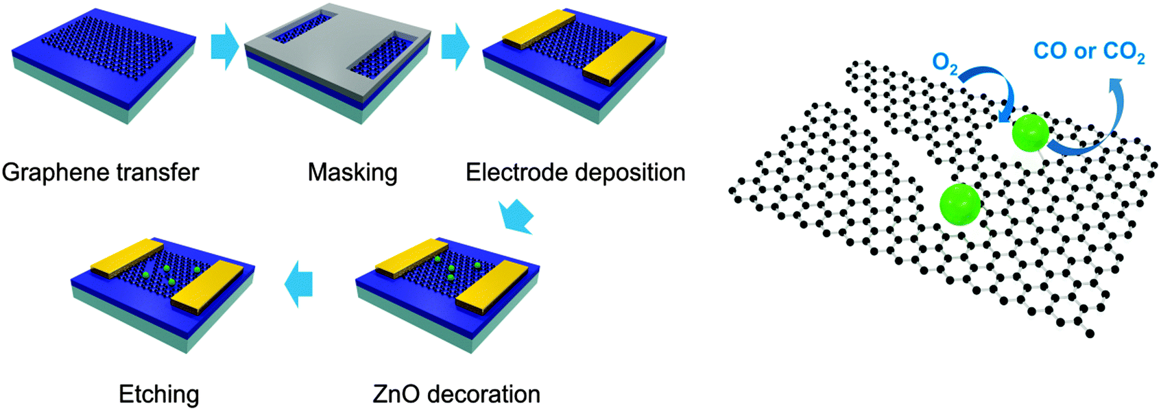 | ||
| Fig. 1 Schematic diagrams of etching graphene on FET. Graphene is etched at 250 °C under an Ar atmosphere by the solid-state reaction between ZnO and C (oxidation: ZnO + C → Zn + CO or CO2, reduction: Zn + 1/2O2 → ZnO). | ||
The structure of monolayer graphene is exactly the same as the honeycomb structure. Thus, graphene etching means a partial destruction of the honeycomb structure of graphene, leading to the decrease in the conductance of graphene. This phenomenon is corresponding to the two dimensional percolation in the honeycomb lattice. Hence, the change of electrical properties by the vacancy creation in graphene can be analysed by bond percolation theory in a honeycomb structure. To date, few efforts have been made to clarify if the evolution of vacancy in graphene obeys the two dimensional percolation theory of the honeycomb lattice. FET is employed to collect the conductivity of etched graphene for percolation analysis in sp2 carbon networks as well as to prove the effect of etching graphene indirectly. By using data measured from FET, we report C–C bonding percolation in graphene.
Finally, patterning was realized easily by carbon gasification under an air atmosphere at low temperature. This carbon gasification can substitute carbon hydrogenation reaction where graphene is etched by catalytic reaction at high temperature under a H2 atmosphere.
Results and discussion
Effect of catalytic etching on monolayer graphene
To see the effect of density of NPs on etching, we prepared two concentrations (1 and 8 mM) of Zn precursor solutions. After the whole etching processes were completed by using each solution under an Ar atmosphere, the etched structures on monolayer graphene were investigated by scanning electron microscopy (SEM) as shown in Fig. 2. The figure shows that multi-carbon vacancies are created in the shape of channels and pits after etching the monolayer graphene sheet. Fig. 2(a) displays a few channels etched by low concentration of precursor solution. The channel width is approximately 650 nm and the shape of the channel is a straight line crossing each other. This is exactly the same etched structure reported on graphene etching by carbon hydrogenation (C + 2H2 → CH4).25–28Fig. 2(b) shows another etched channel which exists solely in graphene. The channel width was measured to be 600 nm. Interestingly, we can see a NP (indicated with a dashed circle) at the end of the etched channel. It can be deduced that the NP contributed to the creation of one channel via catalytic reaction. Meanwhile, Fig. 2(c) exhibits a lot of etched channels created by a high concentration of the precursor solution. Different from Fig. 2(a) and (b), wider channels have been formed in an irregular pattern. However, we can also see that bigger NPs are present at the end of the etched channel, and the phenomenon is in good agreement with the results shown in Fig. 2(b). It is thought that the high concentration solution resulted in agglomerated NPs, which led to a wide channel. Fig. 2(d) exhibits a different shape of the etched structure from the channel where the high concentration of solution was used for etching. Various diameters of pits are observed on etched graphene, and the diameter ranges from 400 nm to 1 µm. The vacancies in the etched channels are apparent evidence of missing C atoms of the graphene sheet. This clearly indicates that graphene was etched by carbon gasification via decorated particles (ZnO + C → Zn + CO or CO2), leading to multi-carbon vacancies. Also, it can be surely concluded that the etched structures of a pit were formed by ZnO NPs during annealing for the solid-state reaction between ZnO and C. These results are consistent with previous work reporting that reduction of NiO by C cuts MWCNTs into pieces (NiO + C → Ni + CO or CO2).31 However, in this case, the solid-state reaction between NiO and C occurred at 900 °C which is much higher than the temperature (250 °C) in this work. For the reduced Zn NPs to etch graphene continuously, we exposed the etched sample to the air for one night (oxidation: Zn + 1/2O2 → ZnO). | ||
| Fig. 2 SEM images of etched graphene by ZnO. The structures in the shape of a channel (a–c) and a pit (d) appear after the etching process. ZnO NPs are located at the end of the etched channel or inside a pit (see inset). Various channels with different widths are created on graphene, depending on the diameter of ZnO NPs. | ||
For a specific analysis about the shape of etched structures and NPs, atomic force microscopy (AFM) analysis was performed on the fully etched monolayer graphene by using high concentration solution. Similar to the images obtained in SEM analysis, the graphene sheet was randomly etched by the solid-state reaction between graphene and catalyst NPs. The graphene in Fig. 3(a) is decorated with ZnO NPs, where some NPs are located at the edge of etched structures. This is clear from the magnified AFM images displayed in Fig. 3(b) and (c). Taking a closer look at Fig. 3(a), it is shown that the etched channel gradually becomes narrow toward the end with NPs. We think that NPs continuously become small due to the reduction of the graphene layer by C.
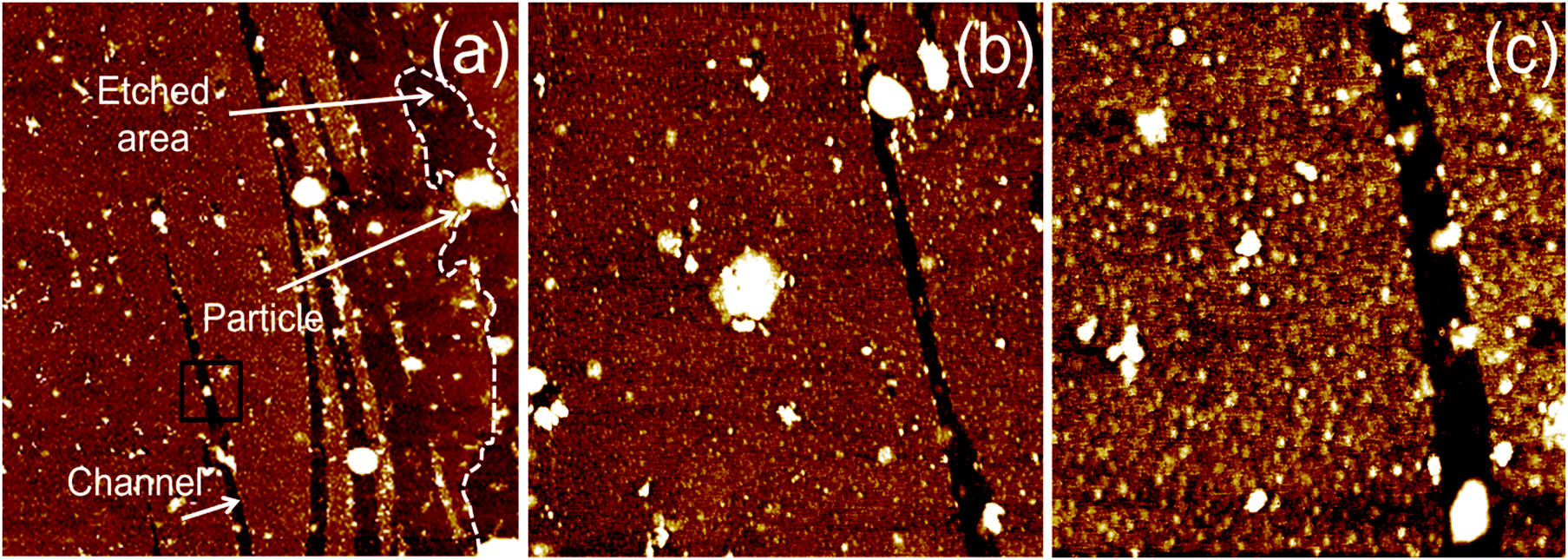 | ||
| Fig. 3 AFM images of fully etched graphene: (a) 10 µm × 10 µm, (b) 5 µm × 5 µm, and (c) 2.5 µm × 2.5 µm. As shown in (a), channels gradually become narrow toward the end with the presence of NPs. This strongly means that the channel was created by ZnO NPs via carbon gasification. | ||
Fig. 3(a) shows that monolayer graphene on the right side is etched irregularly, and the etched edge is marked with a dotted line. Different from the previous studies on graphene etching via carbon hydrogenation, a regular shape of the etched structures was not found in any microscopic analysis of this study. It can be attributed to the number of graphene layers and the surface roughness of the silicon oxide layer. It has been reported that ZnO NPs do not move toward the crystallographic direction on graphite during carbon gasification reaction.31 Furthermore, catalytic etching of single layer graphene is influenced by substrate morphology, leading to irregular nano-patterns.37
XPS analysis
X-ray photoelectron spectroscopy (XPS) analysis can clarify a change of sp2-hybridized carbon into other states and the oxidation state of the Zn element. Hence, to investigate the valence state of C and Zn elements, XPS analysis was conducted on the surface of graphene in the channel of FETs before and after the whole etching process. Fig. 4(a) shows the wide scan of XPS spectra obtained from the fully etched graphene by ZnO. As seen in the figure, peaks corresponding to C, O and Zn elements appear in the wide scan, but the N element was not detected. It means that the precursor was totally transformed into metal oxide through thermal calcination to form ZnO NPs on graphene. The strong peak of O 1s could be attributed to oxygen originating from the SiO2 as a dielectric layer of the FETs, or partially to ZnO NPs. To clarify the valence state of the Zn element, core level spectra were also obtained from monolayer graphene after etching. Fig. 4(b) represents the core level spectra of Zn 2p after etching graphene under an Ar atmosphere. Two major peaks are observed at the binding energies of 1022 and 1045.1 eV, which correspond to Zn 2p3/2 and Zn 2p1/2, respectively. According to the NIST standard reference database, these binding energies correspond to the values of Zn and ZnO.38 Because of this ambiguity, the value of spin orbit splitting is normally used to distinguish the oxidation state between ZnO and Zn. The value of spin orbit splitting in Fig. 4(b) was 23.1 eV which is the same result reporting on the valence state of the Zn metal.39 This strongly means that carbon oxidation by ZnO NPs successfully occurred at 250 °C under an Ar atmosphere, leading to etched structures on monolayer graphene. In Fig. 4(b), a shoulder is seen at the binding energies of 1021 and 1044 eV so that deconvolution was performed on two spectra corresponding to Zn 2p3/2 and Zn 2p1/2. The difference between those binding energies is 23.0 eV, which corresponds to the same value obtained from ZnO.39 This means that the Zn element partially exists in the form of ZnO. Therefore, it is considered that the exposure of reduced ZnO to air is important in order to obtain its oxidation state. | ||
| Fig. 4 XPS spectra recorded from pristine and etched graphene: (a) wide scan obtained from the fully etched graphene by ZnO, (b) the core level spectra of Zn 2p after etching graphene, and the core level spectra of C 1s from (c) pristine graphene and (d) etched graphene. | ||
Comparing XPS spectra of C 1s before and after etching clarifies a difference between sp2-hybridized carbon and disordered carbons such as sp3-hybridized carbon or vacancy defect in a honeycomb structure. Fig. 4(c) and (d) present the core level spectra of C 1s before and after carbon oxidation by ZnO. The binding energy of C 1s spectra was calibrated to 284.6 eV. Fig. 4(d) reveals that the shoulders appear at C 1s spectra after etching graphene.
For more detailed information, the core level spectra of C 1s were deconvoluted into five Gaussian peaks, which were centered at 284.3, 284.6, 285.6, 286.7 and 288.9 eV. Those binding energies can be assigned to carbon vacancy, sp2-hybridized carbon, sp3-hybridized carbon, C–O and C![[double bond, length as m-dash]](https://www.rsc.org/images/entities/char_e001.gif) O, respectively.40,41Table 1 summarizes the area ratio of each deconvoluted component before and after etching. As shown in the table, the area of the sp2 component decreased from 71.0 to 34.4% after etching. On the other hand, the etching produced vacancy component of which area is about 37.6% after the completion of the solid-state reaction. The area of vacancy defect before etching is nearly zero in spite of the deconvolution. The components of C–O and CO decreased down to 2.5 and 3.3%, implying that the oxygen was removed by heat treatment under an Ar atmosphere or transformed into CO or CO2 by the etching process. Interestingly, sp3 component increased 1.5 times up to 22.2% by heat treatment for etching. Here, the participation of oxygen in the reaction can be excluded because the reaction occurred under an Ar atmosphere. This strongly suggests that the dangling bond, which was created by catalytic etching,40 and ZnO decoration mainly contributed to the increase of sp3 component.42 These results mean that carbon atoms in the graphene could be etched, resulting in breaking the symmetry of sp2-hybridized and vacancy carbon atoms.
O, respectively.40,41Table 1 summarizes the area ratio of each deconvoluted component before and after etching. As shown in the table, the area of the sp2 component decreased from 71.0 to 34.4% after etching. On the other hand, the etching produced vacancy component of which area is about 37.6% after the completion of the solid-state reaction. The area of vacancy defect before etching is nearly zero in spite of the deconvolution. The components of C–O and CO decreased down to 2.5 and 3.3%, implying that the oxygen was removed by heat treatment under an Ar atmosphere or transformed into CO or CO2 by the etching process. Interestingly, sp3 component increased 1.5 times up to 22.2% by heat treatment for etching. Here, the participation of oxygen in the reaction can be excluded because the reaction occurred under an Ar atmosphere. This strongly suggests that the dangling bond, which was created by catalytic etching,40 and ZnO decoration mainly contributed to the increase of sp3 component.42 These results mean that carbon atoms in the graphene could be etched, resulting in breaking the symmetry of sp2-hybridized and vacancy carbon atoms.
| Component | Concentration [%] | |
|---|---|---|
| Before etching | After etching | |
| Vacancy defect | 0.0 | 37.6 |
| sp2-hybridized carbon | 71.0 | 34.4 |
| sp3-hybridized carbon | 14.7 | 22.2 |
| C–O | 9.1 | 2.5 |
| CO |
5.2 | 3.3 |
Raman spectroscopy analysis
Raman spectroscopy is used to clearly confirm the numbers of graphene layers and to quantify the degree of sp2-hybridized carbon on the graphene sheet.43 G-band spectra around 1580 cm−1 are related to sp2-hybridized carbon while the D-band around 1350 cm−1 is associated with defects or disorder in graphene. In addition, 2D-band spectra appear at around 2700 cm−1 as overtone of the D-band. In general, the R-value is defined as the intensity ratio of the D-band to G-band spectra and this enables the estimation and quantification of the defectiveness of graphene. Moreover, the intensity ratio of G- and 2D-bands gives the information about the number of layers in the graphene sheet. Fig. 5 displays the Raman spectra of pristine and fully etched graphene. The figure clearly indicates that the intensity ratio of the G-band to the 2D-band is 0.5 which is a feature shown in monolayer graphene.43 This means that monolayer graphene was successfully grown in the Ge substrate and transferred to the SiO2/Si substrate. The D-band shown in pristine graphene could be attributed to the grain boundaries formed during graphene growth.44,45 The other possibility is the presence of oxygen on pristine graphene as shown in XPS analysis. Fig. 5 indicates that the R-value increased from 0.07 to 0.36 after etching processes. In addition, the D′-band, which is also related to defect of graphene, and G-band spectra are merged after the completion of the solid-state reaction. This strongly means that the density of defect increased dramatically in the monolayer graphene sheet.46,47 Commonly, it has been reported that the full width at half maximum (FWHM) of the G-band became broad when the symmetry in a honeycomb structure was broken and that graphene was converted to amorphous carbon when FWHM has the value of 200–300 cm−1.48,49 The FWHM of the G-band in Fig. 5 still has the value less than 100 cm−1 even after etching graphene fully. This indicates that monolayer graphene still keeps crystalline rather than amorphous carbon. | ||
| Fig. 5 Raman spectra of pristine and fully etched monolayer graphene. The R-value increased from 0.07 to 0.36 after etching processes. | ||
I–V characteristics with percolation theory
To monitor the evolution of etching on monolayer graphene, current–voltage characteristics were measured from the FETs after every etching process. Fig. 6 shows the plot of conductance of graphene sheet versus the number of catalytic etching. Unexpectedly, the conductance of graphene decreased after heat treatment at 250 °C under an Ar atmosphere to form ZnO NPs from the precursor. It can be attributed to the vacancy creation by the solid-state reaction between ZnO and C. It has been reported that Zn(NO3)2·6H2O starts decomposing into ZnO from 150 to 250 °C under an inert gas atmosphere (Zn(NO3)2 → ZnO + NOx).50 It is thought that the precursor was thermally decomposed into ZnO NPs during the decoration process. Therefore, it is inferred that graphene was partially etched by ZnO NPs, which was formed below 250 °C (ZnO + C → Zn + CO or CO2). As etching proceeds successively, the conductance of FETs exponentially decreases from 79 mS to 8 µS. It is out of question that monolayer graphene was etched by the solid-state reaction between ZnO and C despite the fact that the reaction occurred under an Ar atmosphere. Fig. 6(b) reveals that the decrease of normalized transconductance represents the same tendency as conductance shows in Fig. 6(a), meaning that gate dependence is hardly influenced by etching monolayer graphene. It can be explained that as shown in SEM images, the area of monolayer graphene is still relatively large in spite of carbon vacancies by a series of etching processes. | ||
| Fig. 6 (a) Normalized conductance as a function of the number of etching. The data were fitted to a line (red) to obtain a critical exponent. (b) Normalized transconductance (gm/VDS) as a function of the number of etching at VDS = 500 mV. | ||
The trend in conductance variation is similar to percolation phenomena in a two-dimensional film. According to the previous studies, the gradual decline in conductance was analyzed by bond percolation.51,52 Therefore, the decrease of conductance can be interpreted by bond percolation theory in a honeycomb structure. In this study, the relationship between conductance and carbon vacancy can be expressed using the following equation:

| Critical exponent (t) | R-square |
|---|---|
| 1.1 | 0.95 |
| 1.2 | 0.96 |
| 1.3 | 0.97 |
| 1.4 | 0.98 |
Finally, in order to demonstrate the usefulness of catalytic etching by carbon oxidation, monolayer graphene was patterned by using ZnO NPs. Fig. 7(a) displays monolayer graphene with an Al mask on the SiO2/Si substrate, where a dotted line is marked at the edge of graphene. The Al-masked samples were oxidized in air at 300 °C for 2 h with the ZnO catalyst to accelerate the catalytic reaction of the etching process. Then, the substrate with patterned graphene was dipped in deionized water to remove unmasked graphene on the SiO2/Si substrate. Fig. 7(b) exhibits an optical image of well-patterned monolayer graphene after etching. This shows that graphene can be patterned to various shapes by changing the design of the metal mask.
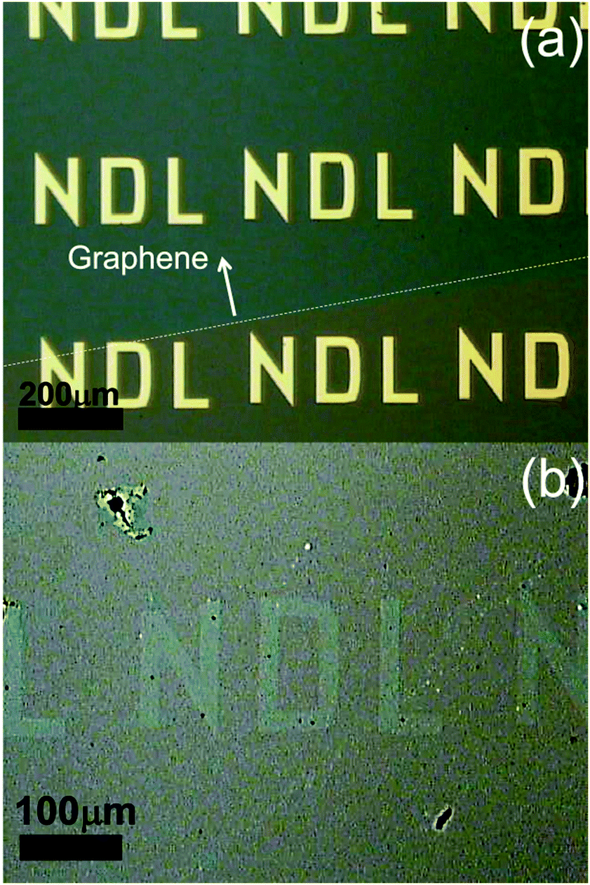 | ||
| Fig. 7 (a) Metal mask deposited on monolayer graphene for patterning. The dotted line was put at the edge of monolayer graphene on the SiO2/Si substrate. (b) Patterned monolayer graphene formed by carbon gasification in air. | ||
Conclusions
In conclusion, we have demonstrated that graphene can be etched at low temperature by catalytic carbon gasification. The morphological information of etched graphene was obtained by SEM and AFM analysis. It was revealed that after the completion of the solid-state reaction between ZnO and C, monolayer graphene had a lot of etched structures in the shape of pits and channels. XPS analysis confirmed the presence of ZnO and the Zn metal, and strongly supported that ZnO NPs were involved in the etching of carbon gasification. Raman spectra also showed that the degree of defects increased with the repetition of catalytic etching. The evolution of vacancies was confirmed by monitoring the conductance of graphene after each step of catalytic etching. In addition, the conductance of etched graphene was analyzed with percolation theory in a honeycomb structure. As a result, the experimental value of critical exponent is 1.4, which is close to the theoretical value. Finally, the pattern of etched graphene was successfully obtained by heating Al-masked graphene under an air atmosphere in the presence of ZnO NPs. Also, this work highlights the possibility of destroying the honeycomb structure when graphene is exposed to heat with metal or metal oxide impurities from Cu or Ni foil.Experimental
Synthesis of monolayer graphene and FET fabrication
Monolayer graphene was synthesized on a poly-crystalline Ge substrate using a CVD method described in ref. 54 and 55. In the process of transfer, the dry transfer method using a thin metal film was employed to prevent organic contamination.55 The graphene sheet was transferred on a heavily p-doped silicon substrate with 300 nm SiO2 so that the back gate can be available. Pt with a thickness of 100 nm was deposited as source/drain contacts by using metal masks to avoid impurity contamination.Etching process of graphene with ZnO
Zn(NO3)2·6H2O (Aldrich, 98%) was adapted as a precursor to decorate monolayer graphene with ZnO NPs. 6 and 50 mg of Zn(NO3)2·6H2O were added in 20 ml of ethanol to prepare low (1 mM) and high (8 mM) concentration solutions. The solutions were sonicated for 15 min to completely dissolve the precursor. Then, 2 (low concentration) and 15 µl (high concentration) of the precursor solutions were separately dropped on monolayer graphene at the channel of FETs. Next, the devices were dried at room temperature until ethanol was evaporated thoroughly. To decorate graphene with ZnO NPs, the FETs were heated in a furnace at 250 °C for 2 h under an Ar atmosphere. In order to etch the graphene sheet on FETs, additional heat treatment was conducted several times using the following method: graphene with ZnO NPs was exposed to air for one night at room temperature and heated under the same conditions to etch graphene by the solid-sate reaction between C and ZnO (ZnO + C → Zn + CO or CO2). After this treatment, the devices were again stagnated in air for one night for the reduced Zn to be oxidized (Zn + 1/2O2 → ZnO) and heated again at 250 °C for 2 h under an Ar atmosphere to further develop the etched structures on the graphene sheet. This process was repeated 5 times to develop the etched structures.Characterization of the etched graphene
The morphological change of graphene was observed after etching using an optical microscope (OLYMPUS, BX41M and U-CMAD3) and a scanning electron microscope (TESCAN, MIRA 3 FEG SEM). For more specific information, an atomic force microscope (Park Systems, Park XE100) was also conducted to examine an etched structure of monolayer graphene and the distribution of ZnO NPs. X-ray photoelectron spectroscopy analysis (Ulvac-PHI, PHI 5000 VersaProbe) was carried out to investigate the oxidation state of C and Zn elements before and after the etching process. Raman spectroscopy (HORIBA JOBIN YVON, HR800-UV) using Ar laser excitation at 514.5 nm was employed to study the degree of defectiveness. To characterize the electrical properties of graphene on FETs by vacancy evolution, current–voltage characteristics were measured using a semiconducting parameter analyzer (Agilent, 4155C) after each etching process.Patterning of monolayer graphene
Monolayer graphene was transferred to the SiO2/Si substrate, and Al (thickness: 20 nm) was deposited on graphene as a mask to protect the masked region of graphene. Next, the sample was heated at 300 °C for 2 h in air after dropping precursor solution on the masked graphene. After the completion of the solid-state reaction for etching, the sample was dipped into deionized water and then dipped in tetramethyl ammonium hydroxide 3 wt% solution to remove other graphene pieces and the Al mask. Finally, well-patterned graphene was formed on the SiO2/Si substrate.Acknowledgements
This work was supported by the second stage of the Brain Korea 21 Plus Project in 2014.Notes and references
- R. R. Nair, P. Blake, A. N. Grigorenko, K. S. Novoselov, T. J. Booth, T. Stauber, N. M. R. Peres and A. K. Geim, Science, 2008, 320, 1308 CrossRef CAS PubMed.
- K. S. Kim, Y. Zhao, H. Jang, S. Y. Lee, J. M. Kim, K. S. Kim, J.-H. Ahn, P. Kim, J.-Y. Choi and B. H. Hong, Nature, 2009, 457, 706–710 CrossRef CAS PubMed.
- C. Lee, X. Wei, J. W. Kysar and J. Hone, Science, 2008, 321, 385–388 CrossRef CAS PubMed.
- A. A. Balandin, S. Ghosh, W. Bao, I. Calizo, D. Teweldebrhan, F. Miao and C. N. Lau, Nano Lett., 2008, 8, 902–907 CrossRef CAS PubMed.
- K. S. Novoselov, A. K. Geim, S. V. Morozov, D. Jiang, Y. Zhang, S. V. Dubonos, I. V. Grigorieva and A. A. Firsov, Science, 2004, 306, 666–669 CrossRef CAS PubMed.
- Y. Zhang, Y.-W. Tan, H. L. Stormer and P. Kim, Nature, 2005, 438, 201–204 CrossRef CAS PubMed.
- X. Wang, L. Zhi and K. Mullen, Nano Lett., 2008, 8, 323–327 CrossRef CAS PubMed.
- X. Li, H. Zhu, K. Wang, A. Cao, J. Wei, C. Li, Y. Jia, Z. Li, X. Li and D. Wu, Adv. Mater., 2010, 22, 2743–2748 CrossRef CAS PubMed.
- J. Wu, M. Agrawal, H. A. Becerril, Z. Bao, Z. Liu, Y. Chen and P. Peumans, ACS Nano, 2010, 4, 43–48 CrossRef CAS PubMed.
- J. Meyer, P. R. Kidambi, B. C. Bayer, C. Weijtens, A. Kuhn, A. Centeno, A. Pesquera, A. Zurutuza, J. Robertson and S. Hofmann, Sci. Rep., 2014, 4, 5380 CAS.
- I.-Y. Lee, H.-Y. Park, J.-H. Park, G. Yoo, M.-H. Lim, J. Park, S. Rathi, W.-S. Jung, J. Kim, S.-W. Kim, Y. Roh, G.-H. Kim and J.-H. Park, Nanoscale, 2014, 6, 3830–3836 RSC.
- Y. Wang, L. Wang, T. Yang, X. Li, X. Zang, M. Zhu, K. Wang, D. Wu and H. Zhu, Adv. Funct. Mater., 2014, 24, 4666–4760 CrossRef CAS.
- K. Carva, B. Sanyal, J. Fransson and O. Eriksson, Phys. Rev. B: Condens. Matter Mater. Phys., 2010, 81, 245405 CrossRef.
- J. J. Palacios, J. Fernandez-Rossier and L. Brey, Phys. Rev. B: Condens. Matter Mater. Phys., 2008, 77, 195428 CrossRef.
- C. S. Park, Y. Zhao, J.-H. Lee, D. Whang, Y. Shon, Y.-H. Song and C. J. Lee, Appl. Phys. Lett., 2013, 102, 032106 CrossRef.
- M. Y. Han, B. Ozyilmaz, Y. Zhang and P. Kim, Phys. Rev. Lett., 2007, 98, 206805 CrossRef PubMed.
- L. Jiao, L. Zhang, X. Wang, G. Diankov and H. Dai, Nature, 2009, 458, 877–880 CrossRef CAS PubMed.
- F. Guinea, M. I. Katsnelson and M. A. H. Vozmediano, Phys. Rev. B: Condens. Matter Mater. Phys., 2008, 77, 075422 CrossRef.
- J. Bai, X. Zhong, S. Jiang, Y. Huang and X. Duan, Nat. Nanotechnol., 2010, 5, 190–194 CrossRef CAS PubMed.
- D. V. Kosynkin, A. L. Higginbotham, A. Sinitskii, J. R. Lomeda, A. Dimiev, B. K. Price and J. M. Tour, Nature, 2009, 458, 872–876 CrossRef CAS PubMed.
- A. L. Elías, A. R. Botello-Méndez, D. Meneses-Rodríguez, V. J. González, D. Ramírez-González, L. Ci, E. Muñoz-Sandoval, P. M. Ajayan, H. Terrones and M. Terrones, Nano Lett., 2010, 10, 366–372 CrossRef PubMed.
- J. Wang, L. Ma, Q. Yuan, L. Zhu and F. Ding, Angew. Chem., Int. Ed., 2011, 50, 8041–8045 CrossRef CAS PubMed.
- S. Fujii and T. Enoki, J. Am. Chem. Soc., 2010, 132, 10034–10041 CrossRef CAS PubMed.
- L. Ma, J. Wang and F. Ding, Angew. Chem., Int. Ed., 2012, 51, 1161–1164 CrossRef CAS PubMed.
- L. Ci, L. Song, D. Jariwala, A. L. Elias, W. Gao, M. Terrones and P. M. Ajayan, Adv. Mater., 2009, 21, 4487–4491 CrossRef CAS.
- S. S. Datta, D. R. Strachan, S. M. Khamis and A. T. C. Johnson, Nano Lett., 2008, 8, 1912–1915 CrossRef CAS PubMed.
- L. Ma, J. Wang, J. Yip and F. Ding, J. Phys. Chem. Lett., 2014, 5, 1192–1197 CrossRef CAS PubMed.
- W. Baaziz, G. Melinte, O. Ersen, C. Pham-Huua and I. Janowska, Phys. Chem. Chem. Phys., 2014, 16, 15988–15993 RSC.
- L. Gao, W. Ren, B. Liu, Z.-S. Wu, C. Jiang and H.-M. Cheng, J. Am. Chem. Soc., 2009, 131, 13934–13936 CrossRef CAS PubMed.
- L. Zhang, S. Diao, Y. Nie, K. Yan, N. Liu, B. Dai, Q. Xie, A. Reina, J. Kong and Z. Liu, J. Am. Chem. Soc., 2011, 133, 2706–2713 CrossRef CAS PubMed.
- D. W. McKee, Carbon, 1970, 8, 623–635 CrossRef CAS.
- Z. J. Pan and R. T. Yang, J. Catal., 1991, 130, 161–172 CrossRef CAS.
- X. X. Wang, J. N. Wang, L. F. Su and J. J. Niu, J. Mater. Chem., 2006, 16, 4231–4234 RSC.
- D.-H. Kim and K. Waki, J. Nanosci. Nanotechnol., 2010, 10, 2375–2380 CrossRef CAS PubMed.
- S. Y. Lee, D.-H. Kim, S. C. Choi, D.-J. Lee, J. Y. Choi and H.-D. Kim, Microporous Mesoporous Mater., 2014, 194, 46–51 CrossRef CAS.
- W. L. Holstein and M. Boudart, Fuel, 1983, 62, 162–165 CrossRef CAS.
- T. Tsukamoto and T. Ogino, J. Phys. Chem. C, 2011, 115, 8580–8585 CAS.
- NIST X-ray Photoelectron Spectroscopy Database, Version 4.1, National Institute of Standards and Technology, Gaithersburg, 2012.
- C. Wagner and G. Muilenberg, Handbook of X-ray photoelectron spectroscopy, Perkin-Elmer, 1979, p. 84 Search PubMed.
- H. Estrade-Szwarckopf, Carbon, 2004, 42, 1713–1721 CrossRef CAS.
- A. Barinov, O. B. Malcioglu, S. Fabris, T. Sun, L. Gregoratti, M. Dalmiglio and M. Kiskinova, J. Phys. Chem. C, 2009, 113, 9009–9013 CAS.
- A. Velamakanni, C. W. Magnuson, K. J. Ganesh, Y. Zhu, J. An, P. J. Ferreira and R. S. Ruoff, ACS Nano, 2010, 4, 540–546 CrossRef CAS PubMed.
- A. C. Ferrari, J. C. Meyer, V. Scardaci, C. Casiraghi, M. Lazzeri, F. Mauri, S. Piscanec, D. Jiang, K. S. Novoselov, S. Roth and A. K. Geim, Phys. Rev. Lett., 2006, 97, 187401 CrossRef CAS PubMed.
- I. Vlassiouk, M. Regmi, P. Fulvio, S. Dai, P. Datskos, G. Eres and S. Smirnov, ACS Nano, 2011, 5, 6069–6076 CrossRef CAS PubMed.
- X. Li, C. W. Magnuson, A. Venugopal, J. An, J. W. Suk, B. Han, M. Borysiak, W. Cai, A. Velamakanni, Y. Zhu, L. Fu, E. M. Vogel, E. Voelkl, L. Colombo and R. S. Ruoff, Nano Lett., 2010, 10, 4328 CrossRef CAS PubMed.
- L. G. Cancado, A. Jorio, E. H. Martins Ferreira, F. Stavale, C. A. Achete, R. B. Capaz, M. V. O. Moutinho, A. Lombardo, T. S. Kulmala and A. C. Ferrari, Nano Lett., 2011, 11, 3190–3196 CrossRef CAS PubMed.
- M. M. Lucchese, F. Stavale, E. H. Martins. Ferreira, C. Vilani, M. V. O. Moutinho, R. B. Capaz, C. A. Achete and A. Jorio, Carbon, 2010, 48, 1592–1597 CrossRef CAS.
- A. C. Ferrari and J. Robertson, Phys. Rev. B: Condens. Matter Mater. Phys., 2000, 61, 14095 CrossRef CAS.
- A. C. Ferrari and J. Robertson, Phys. Rev. B: Condens. Matter Mater. Phys., 2001, 64, 075414 CrossRef.
- J. Chen, Z. Feng, P. Ying, M. Li, B. Han and C. Li, Phys. Chem. Chem. Phys., 2004, 6, 4473–4479 RSC.
- B. J. Last and D. J. Thouless, Phys. Rev. Lett., 1971, 27, 1719 CrossRef CAS.
- M. Sahimi, B. D. Hughes, L. E. Scriven and H. T. Davis, J. Phys. C: Solid State Phys., 1983, 16, L521–L527 CrossRef CAS.
- E. E. Vogel, W. Lebrecht and J. F. Valdes, Physica A, 2010, 389, 1512–1520 CrossRef CAS.
- G. Wang, M. Zhang, Y. Zhu, G. Ding, D. Jiang, Q. Guo, S. Liu, X. Xie, P. K. Chu, Z. Di and X. Wang, Sci. Rep., 2013, 3, 2465 Search PubMed.
- J.-H. Lee, E. K. Lee, W.-J. Joo, Y. Jang, B.-S. Kim, J. Y. Lim, S.-H. Choi, S. J. Ahn, J. R. Ahn, M.-H. Park, C.-W. Yang, B. L. Choi, S.-W. Hwang and D. Whang, Science, 2014, 344, 286–289 CrossRef CAS PubMed.
| This journal is © the Owner Societies 2016 |